 Sachin Sharma†
 Rajesh V. Nair
- Laboratory for Nano-scale Optics and Meta-Materials (LaNOM), Department of Physics, Indian Institute of Technology Ropar, Ropar, Punjab, India
The defect centers in solid-state materials especially the nitrogen-vacancy (NV) centers in diamond have shown a tremendous potential for their utilization in quantum technology applications. However, they exhibit certain drawbacks such as the feeble zero phonon line with huge phonon contribution and the higher lifetime values. Here, we present a novel approach to control the spontaneous emission from NV centers in nanodiamond using engineered self-assembled photonic crystals. Using two complimentary emission measuring geometries at room temperature, we show a 63% suppression and 17% enhancement of NV center emission intensity using photonic stopgap, supported with simulations. The emission rates are modified in a broad spectral range of NV center emission and are consistent with the Barnett–Loudon sum rule. The results are crucial for emerging quantum technologies using NV centers in diamond.
Introduction
Atomic scale defects in wide bandgap materials have gained prominence over the past few years due to their unique optical and spin properties (Aharonovich et al., 2016). These defects generally exist as point defects within otherwise perfect crystal and create the defect states within the bandgap of the host material. These states can be excited by optical or electrical means, and they emit radiation corresponding to the visible or infrared region of the electromagnetic spectrum (Grotz et al., 2012; Mizuochi et al., 2012). Hence, they are also called color centers, and materials such as diamond shows beautiful hues. The isolated nature of these defect centers makes them an ideal candidate as a single photon source at room temperature, which is one of the fundamental building blocks of quantum technologies (Atatüre et al., 2018; Awschalom et al., 2018). Other solid-state emitters such as quantum dots suffer from photoblinking and photobleaching, besides being operational at ultra-low temperature (Buckley et al., 2012). Also, the defect centers generally exhibit long spin coherence times, which makes them stand apart in comparison to other solid-state emitters (Schröder et al., 2016).
Among the defect centers in wide bandgap materials, the defects in diamond and particularly the nitrogen-vacancy (NV) center has gained a lot of attention (Doherty et al., 2013). The NV center is a point defect, which is formed in a diamond crystal when a substitutional nitrogen atom occupies the site adjacent to a vacancy in a diamond crystal, as shown in Figure 1A. The NV center exists mainly in two charge states, namely, the neutral charge state (NV0) and the negative charge state (NV−) (Shields et al., 2015). The NV0 is a system of five electrons, three of which are contributed by the dangling bonds around the vacancy and two are contributed from the lone pair of nitrogen. It has total spin S = ½ and has a singlet ground state 2E and a singlet excited state 2A2, with an energy gap of 2.15 eV, as shown in Figure 1B (Felton et al., 2008; Barson et al., 2019). The NV− also has the similar configuration as that of NV0 except that it contains an extra electron acquired from a nearby donor atom, which makes it an even electron system containing six electrons. It has total spin S = 1, which leads to its triplet ground state (3A2) and triplet excited state (3E) with an energy gap of 1.945 eV. A total of two metastable state (1A and 1E) with an energy gap of 1.19 eV, also known to exists between 3A2 and 3E, as shown in Figure 1C (Rogers et al., 2015).
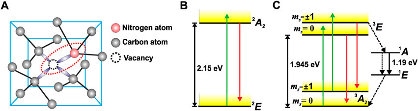
FIGURE 1. (A) The diamond structure containing a carbon vacancy and a substitutional nitrogen atom forming NV center. (B) The energy level diagram of NV0 center with a ground state (2E) and an excited state (2A2). (C) The energy level diagram of NV− center with a triplet ground state (3A2), an excited state (3E), and metastable states (1A and 1E).
The spontaneous emission from defect centers is generally characterized by two types of transitions, namely, the zero phonon line (ZPL) and the phonon sideband (PSB). The ZPLs are the pure electronic transitions from a lowest vibration level of the excited state to the lowest vibration level of the ground state. The width of ZPL represents lifetime-limited line-width at cryogenic temperature (Shen et al., 2008). However, as the temperature is increased, the ZPL is broadened by orders of magnitude. Thus, it is highly required to obtain the color centers with high intensity and narrow linewidths (Wolters et al., 2010). On the other hand, the PSB transitions in the emission spectra corresponds to transitions from the lowest vibration level of the excited state to the higher vibration level of the ground state. These transitions are red-shifted with respect to the ZPL in the emission spectra and blue-shifted in the absorption spectra. These transitions are mediated by lattice phonons called the phonon-mediated transitions, which is incoherent in nature and need to be suppressed. The amount of PSB transitions present in the emission spectra is described using the Debye–Waller (DW) factor, which is defined as the ratio of intensity at the ZPL to the intensity in the whole emission wavelength range (Zhao et al., 2012). Thus, it is required to increase the DW factor to use NV center efficiently in quantum technologies.
Engineered photonic structures are proposed as a platform to tailor the spontaneous emission from NV centers to suppress the PSB emission and thereby enhance the ZPL line intensity as well as the rate. The coupling of NV centers in a single crystal diamond to photonic waveguide leading to 18% enhancement in the ZPL emission rate has been demonstrated at low temperature (∼6 K) (Barclay et al., 2011). It is noted that even at low temperature, the complete suppression of PSB is not achieved and the DW factor value is quite low about ∼3% (Santori et al., 2010; Zhao et al., 2012). Another approach which utilizes coupling of nanodiamonds containing NV centers to silver nanowires exhibiting surface plasmon modes has realized ∼5× enhancement in the emission rate (Kumar et al., 2013). Such schemes require the deterministic positioning of nanodiamonds in the vicinity of the plasmonic structure, which is done using sophisticated pick-and-place technique utilizing atomic force microscopy. Therefore, much simpler yet effective routes are required to manipulate the emission intensity and rate of the NV centers.
Photonic crystals offer a simplistic solution to achieve a significant control over emission intensity and rate. Photonic crystals are artificially engineered structures which possess a periodic variation of the refractive index in the optical wavelength scale. Photonic crystals are inspired from spectacular colors of butterflies, birds, and beetles, which also possess similar underlying periodic structures (Cersonsky et al., 2021). They have also been utilized for various applications such as anti-counterfeiting technology (Lai et al., 2022). In photonic crystals, the Bragg diffraction of incident light in a particular direction gives rise to forbidden frequency bands called photonic stopgaps. The photon density of the state in a photonic crystal is a function of frequency as well as the spatial position and therefore termed as local density of optical states (LDOS) (Lodahl et al., 2004). The LDOS reduces at the stopgap frequency, whereas at the gap edges, LDOS shows an enhancement with respect to a homogeneous medium (Barth et al., 2005; Nair et al., 2012). This property of photonic crystals has been utilized for controlling spontaneous emission and Raman scattering experiments (Guddala et al., 2012; Priya and Nair, 2019; Khokhar et al., 2020).
In this study, we exercise reliable control over spontaneous emission from ensemble of NV centers in nanodiamonds using the photonic crystals at room temperature. The suppression and enhancement of emission intensity and rate from the same structures is achieved using two complimentary emission measurement geometries. The wavelength-dependent lifetime measurements reveal strong fluctuation in LDOS induced by the spatial-dependent photonic stopgaps. The spectral redistribution of emission lifetime is explained using the Barnett–Loudon sum rule. The results provide a platform to engineer the emission and charge state dynamics of the NV centers in nanodiamonds.
Materials and methods
The nanodiamonds with an average size of 70 nm and containing more than 300 NV centers per nanodiamond are drop casted on the top of self-assembled photonic crystal samples. We fabricated the photonic crystals having lattice constants 277 nm (sample A) and 406 nm (sample B) using the method of colloidal self-assembly of polystyrene microspheres having a refractive index of 1.59. In colloidal self-assembly method, the colloidal suspension of monodisperse microspheres is allowed to evaporate in a temperature-controlled environment, thereby creating self-assembly of microspheres with fcc packing, as detailed in Priya and Nair (2016). We performed the electromagnetic field propagation simulations using the finite difference time domain (FDTD) simulator (Lumerical). The electromagnetic dipoles were placed at the top of designed photonic crystals to mimic the NV center. Figure 2 shows the simulated reflectivity spectra at the normal incidence for sample A (solid black) and sample B (solid red) with reflectivity peak centered at 453 and 664 nm, respectively. The measured reflectivity peak at near-normal incidence, using a spectrophotometer, for sample A (triangles) and sample B (squares) are centered at 445 and 667 nm, respectively. Thus, the experimental reflectivity results are in good agreement with the simulated reflectivity curves. The slight mismatch in the peak wavelength is due to the consideration of normal incidence and ideal sample in the simulation. The emission spectra are measured using a home-built confocal emission setup, as described in Sharma and Nair (2018). In brief, the setup utilizes a frequency doubled Nd-YAG laser (Q-Smart 450; Quantel) to excite the nanodiamonds. The emission light is filtered using a 532-nm dichroic filter and sent to the spectrometer (Isoplane-320; Princeton Instruments) equipped with a CCD camera (PIXIS 100B) which records the intensity as a function of wavelength. The time-resolved emission measurements are performed on a home-built setup consisting of a 532 nm pulsed laser (pulse width: 52 ps, repetition rate: 10 MHz). The sample is excited and the emission is collected through a ×4 objective with a low numerical aperture (NA) of 0.10. It is important to use a low NA objective in our experiments because higher number of K-vectors being probed in a high NA objective may lead to averaging of emission intensity at different angles and the effect of stopgap at normal incidence may not be prominent. The experiments are performed in two complimentary geometries as shown in Figure 3. The collected emission is then passed through a bandpass filter (FF01-660/13-25; Semrock) to allow 660 ± 6 nm to be incident on a single photon detector (PD-100-CTD-FC, Microphoton Devices). The detector is connected with time correlator (HydraHarp 400; PicoQuant) which creates the histogram of time events corresponding to difference between the excitation pulse and photon detection time.
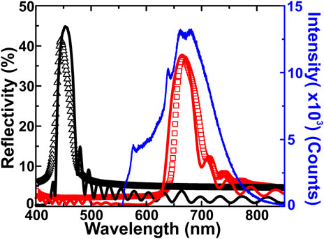
FIGURE 2. The measured emission intensity (right y-axis) from sample A (blue line) featuring ZPL and PSB of NV center. The simulated reflectivity (left y-axis) of sample A (black solid) and sample B (red solid) shows the stopgaps at 453 and 664 nm, respectively. The measured reflectivity of sample A (triangles) and sample B (squares) shows the stopgaps at 445 and 667 nm, respectively.
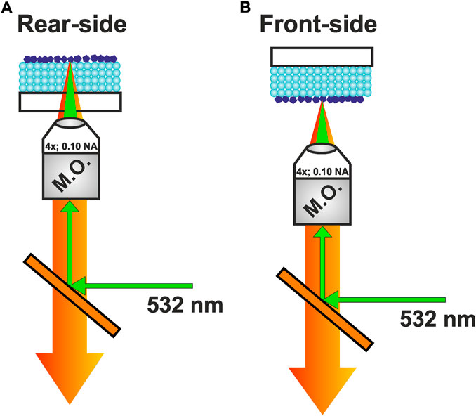
FIGURE 3. (A) and (B) are the rear-side and front-side geometries used in the measurements. The measurement geometries are complimentary to each other. In the rear-side geometry, the nanodiamonds are excited through the substrate side, whereas in the front side geometry the excitation beam directly excites the nanodiamonds decorated on the top of photonic crystals.
Figure 2 also shows the measured emission spectra from NV centers painted on the sample A. The emission spectra feature characteristics ZPL peaks at 576 and 639 nm corresponding to NV0 and NV− centers, respectively along with a PSB emission extends up to 850 nm. The presence of these inherent spectral features confirms that sample A does not induce any spectral changes to the NV center emission. This is expected because the stopgap corresponding to sample A is off-resonant with respect to NV center emission (570–850 nm). Hence, sample A is regarded as the “reference” sample in the following. The PSB emission of NV centers needs to be enhanced or suppressed depending upon the application concerned (Fu et al., 2007; Wolters et al., 2010). For quantum technological applications where it is required to get an indistinguishable single photon source, the PSB emission needs to be suppressed. On the other hand, the biomedical applications and imaging that require PSB emission to be enhanced as it coincides with biologically transparent window. We have used self-assembled photonic crystal as a platform to study the suppression as well as enhancement of PSB emission by utilizing two different measurement geometries, as depicted in Figure 3. In the rear-side geometry, the excitation beam passes through the substrate and photonic crystal before exciting the nanodiamonds and the emission is collected through the same path (Figure 3A). In the front-side geometry, the nanodiamonds decorated on the top of photonic crystals are directly excited by the excitation beam (Figure 3B).
Results
Emission intensity suppression and enhancement
Figure 4A shows the emission spectra from the reference (black) and sample B measured in the rear-side (red) and front-side (blue) geometry. It is noted that for sample B, the respective spectra from the complimentary geometries show contrasting differences in the wavelength range 650–685 nm. The measured spectra from sample B in the rear-side geometry shows strong intensity suppression. However, the measured emission corresponding to the front-side geometry shows an enhancement in the emission intensity with respect to reference sample. It is worth mentioning that measured emission spectra from the reference sample in the complimentary geometries does not show any spectral changes. This confirms that the off-resonant photonic stopgap does not have any effect on the NV center emission spectra.
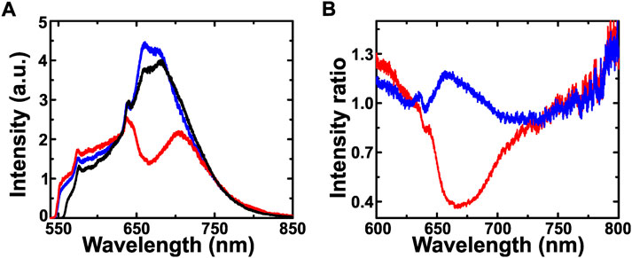
FIGURE 4. (A) The emission spectra of the reference sample (black) showing characteristic ZPLs of NV center charge states (NV0 and NV−) at 576 and 639 nm along with a broad PSB emission. The emission spectra measured from sample B in the rear-side (red) and front-side (blue) geometry. (B) The intensity ratio of the emission from sample B in the rear-side (red) and front-side (blue) geometry with respect to the emission from the reference sample.
The change in emission intensity profile induced by the sample B is described in terms of intensity ratio, which is the ratio of the measured emission intensity from the sample B to the emission intensity from the reference sample. The value of intensity ratio greater than unity implies the enhancement of emission intensity from sample with respect to the reference whereas its value less than unity implies suppression in emission intensity. Figure 4B shows that the intensity ratio corresponding to rear-side measurements from sample B shows a prominent dip centered at 667 nm, which is coincident with its stopgap wavelength. The minimum value of the intensity ratio is 0.37, which amounts to 63% suppression in emission intensity for the rear-side geometry. This intensity suppression in an indication of the decrease in the LDOS at 667 nm due to stopgaps. It is important to note that the suppression of emission intensity due to opacity of photonic crystals can be ruled out here as the intensity of the sample B is compared with the reference sample made up of same material (polystyrene) and having almost same thickness. The intensity ratio corresponding to the front-side geometry shows a peak at 667 nm, which constitute 17% enhancement in emission intensity of sample B with respect to the reference sample. Further, we have simulated the far-field emission intensity profiles for the two geometries for both the samples. The dipole was oriented parallel to substrate in order to achieve maximum emission in perpendicular direction. Perfectly matched layer boundary conditions were used so that reflections from the edges can be avoided. Figures 5A,B show the far field intensity in rear-side geometry and Figures 5C,D show intensity profiles in front-side geometry at 667 nm for the reference sample and sample B, respectively. The far-field intensity for the sample B in the rear-side geometry is suppressed in comparison to the reference sample whereas in the front-side geometry we see an enhancement in the far-field intensity with respect to the reference sample. We note the enhancement in the rear side for the reference sample is merely a substrate effect and is spectrally independent, which is the reason that we do not observe any spectral change in complimentary geometries for the reference sample. But for the sample B we observe enhancement as well as suppression in emission intensity induced by the stopgap. The emission wavelengths corresponding to the stopgap are inhibited to propagate through the sample B and are reflected back in free space towards the monitor in the front side geometry which is the reason for suppression in the rear side geometry and enhancement in the front side geometry. The simulated intensity enhancement and suppression agree reasonably well with the experimental results. Thus, it is concluded that the NV center emission intensity can be deterministically enhanced or suppressed using the photonic crystals.
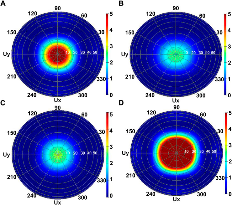
FIGURE 5. (A) and (B) are the far-field emission intensity profiles at 667 nm in rear side geometry for the reference and sample B. (C) and (D) are the far-field emission intensity profiles at 667 nm in front side geometry for the reference and sample B.
Emission decay rate measurements
Figure 6 shows the measured emission decay curve corresponding to the reference sample (triangles) along with decay curve from sample B measured in the rear-side (circles) and front-side (squares) geometry. It is noted that the emission decay of sample B measured in the rear-side geometry is slowed down with respect to the decay curve for the reference sample. However, the decay curve measured in the front-side geometry becomes faster than the reference sample emission decay curve. The decay spectra are fitted with a biexponential decay function, which yields two lifetime components (Kumar et al., 2015). The faster component τ1 arises due to the presence of graphitic impurities whereas the slower component τ2 is the actual lifetime of NV centers. The values of τ1 and τ2 for the reference sample are 4.2 and 20.6 ns, respectively. The corresponding values for sample B measured in rear-side geometry are 4.4 and 22.4 ns, respectively. It is clear that τ2 value obtained for sample B is higher than the same for the reference sample whereas τ1 remains the same. The τ1 and τ2 values for sample B in the front-side geometry are 3.9 and 18.1 ns, respectively. In this case, the τ2 value is lower than the same for the reference sample. Thus, the τ2 for sample B in the rear-side geometry shows an enhancement with respect to the same for the reference sample whereas τ2 value is suppressed for the same sample (sample B) when the measured in the front-side geometry.
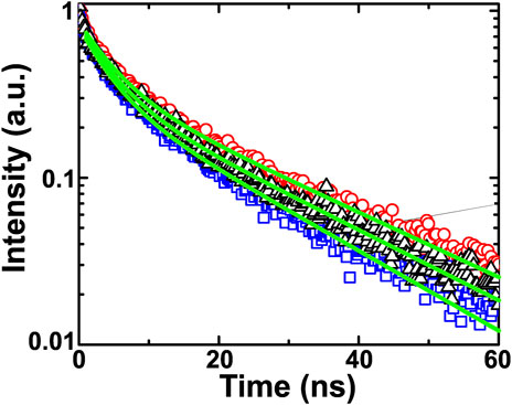
FIGURE 6. The emission decay of the reference sample (triangles) and sample B sample measured in rear-side (circles) and front-side (squares) geometry. The solid lines are the biexponential fit to the respective decay spectra.
Discussion
The statistical nature of emission lifetime impels for the spatial-dependent decay rate measurements. Therefore, we have measured the decay rate from 100 different spatial locations on the same sample. Figure 7A shows the τ1 distribution corresponding to the reference (patterned) and sample B (solid) measured in the rear-side geometry. The distributions are centered at 4.6 ± 0.1 and 4.9 ± 0.1 ns, respectively. It is seen that the distributions have a significant overlap with each other. This is expected because τ1 component of the decay curve arises from graphitic impurities as explained above. Figure 7B depicts the τ2 distribution from the reference (patterned) and sample B (solid) centered at 22.4 ± 0.2 and 23.2 ± 0.4 ns, respectively. It is seen that the distributions have a significant overlap with each other. However, their distinctiveness was checked by the Kolmogorov–Smirnov test which confirmed that the shown lifetime histograms are arising from distinct distributions (Press et al., 2007). The width of distribution corresponding to sample B is 2× greater than the lifetime width for the reference sample. This is attributed due to inherent fluctuation of LDOS in photonic crystals (Priya and Nair, 2019).
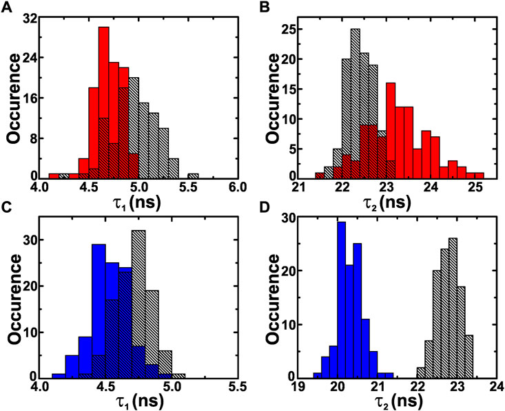
FIGURE 7. (A,B) The τ1 and τ2 distributions corresponding to the reference (patterned) and sample B (red) measured at 660 nm in the rear-side geometry. (C,D) The τ1 and τ2 distributions of the for the reference (patterned) and sample B measured in the front-side geometry.
Figure 7C shows the τ1 distribution corresponding to the reference (patterned) and sample B (solid) measured in the front-side geometry. The distributions are centered at 4.5 ± 0.1 and 4.7 ± 0.1 ns, respectively. As expected, the distributions overlap significantly which indicates that the change of LDOS does not have any effect on the τ1 component of the decay curve. This validates the argument of graphitic origin of τ1 component in the decay curve. Figure 7D shows the τ2 distributions from the reference and sample B measured in the front-side geometry. The distributions are centered at 22.8 ± 0.3 and 20.3 ± 0.3 ns, respectively. Similar to the τ2 distributions obtained in the rear-side, the τ2 distributions for the reference and sample B in the front-side geometry are distinct from each other. The mean value of τ2 distribution for sample B is 11% lower in comparison to the same for the reference sample. This decrease in τ2 value clearly indicates the reduced LDOS for sample B with respect to the reference sample. Thus, it is concluded that the emission rate from NV centers can be modified in both ways (suppressed or enhanced), utilizing the photonic stopgaps by simply changing the measurement geometry.
It is interesting to note that the large bandwidth of NV center emission spectra allows us to observe the LDOS modifications not only at the photonic stopgaps but also at the red-side and blue-side of the stopgap. We have measured the spectral-dependent decay rates from NV centers at different wavelengths: 600 nm (PSB of NV0), 638 nm (PSB of NV0 and ZPL of NV−), and 660 and 700 nm (PSB of NV−). Figure 8A shows the wavelength-dependent variation in τ2 values for the reference (triangles) and sample B (circles) measured in the rear-side geometry. It is seen that the τ2 values decrease with increase in wavelength. This is expected due to different spectral ranges of NV center charge states. The NV0 contribution spans predominantly from 575 to 650 nm whereas the NV− contribution spans predominantly from 637 to 800 nm (Rondin et al., 2010). It is interesting to note that for sample B the τ2 values at 638 and 660 nm are decreased in comparison to the reference. On the contrary, the τ2 values for sample B at 600 and 700 nm are increased with respect to the same for the reference sample. Thus, it can be concluded that the decrease in lifetime due to photonic stopgap is balanced by its enhancement at the wavelengths outside the stopgap. This is completely in-line with the Barnett–Loudon sum rule which states that the suppression or enhancement of emission rate in a specific wavelength range is augmented by the enhancement or suppression at other wavelengths (Barnett and Loudon, 1996). It is also noted that the change in τ2 value is not commensurate with the change in emission intensity (Figure 4). This may be attributed to the contribution of other defect such as graphitic impurities in the decay spectra. These impurities give rise to non-single exponential behavior of the decay spectra and hence the resulted decay spectra is the convolution of the decay spectra from NV center and other impurities. Figure 8B shows the wavelength-dependent τ2 values of the reference and sample B measured in the front-side geometry. Similar to the wavelength-dependent τ2 behavior for the rear-side geometry, the τ2 values in the front-side geometry shows a decrease with an increase in wavelength, ascribed to different charge states (NV0 and NV−) of NV center. The τ2 values at 638 and 660 nm for sample B are lower in comparison to the same for the reference sample, which is expected due to photonic stopgap of sample B. The corresponding τ2 values at 600 and 700 nm for sample B are higher than the same for the reference sample. This is explained using the Barnett–Loudon sum rule and compliment the results obtained from the rear-side geometry.
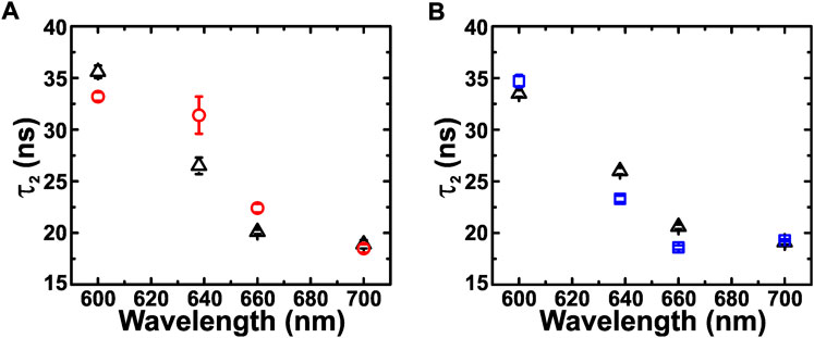
FIGURE 8. (A) The wavelength dependence of τ2 for the reference (triangles) and sample B (circles) measured in the rear-side geometry. (B) The corresponding values of τ2 for the reference (triangles) and sample B (squares) measured in the front-side geometry.
In conclusion, we have demonstrated the control of spontaneous emission of NV centers in nanodiamonds using photonic crystals. Two complimentary measurement geometries are used obtain 63% suppression and 17% enhancement in emission intensity, supported with FDTD simulations. The enhancement and suppression of emission lifetime in the corresponding geometries are also consistent with the emission intensity results. The NV center emission is modified in a wide spectral range according to the redistributed LDOS at different wavelengths, which is in agreement with Barnett–Loudon sum rule. As a future perspective, it will be interesting to observe modification in the single photon emission characteristics from color centers in nanodiamonds using the photonic crystals The results help to make NV center as a robust platform for quantum technologies and biophotonics.
Data availability statement
The original contributions presented in the study are included in the article/Supplementary Material; further inquiries can be directed to the corresponding author.
Author contributions
RN conceived the presented idea. SS performed the experiments. AH performed the simulations. SS, RN, and AH analyzed the results and wrote the manuscript. All authors contributed to the final version of the manuscript.
Funding
The authors would like to acknowledge the financial support from DST-ICPS [DST/ICPS/QuST/Theme-2/2019/General], DST-SERB [SB/SJF/2020-21/05]. RVN acknowledges the Swarnajayanti Fellowship (DST/SJF/PSA-01/2019-20). AH acknowledges the PMRF fellowship.
Conflict of interest
The authors declare that the research was conducted in the absence of any commercial or financial relationships that could be construed as a potential conflict of interest.
Publisher’s note
All claims expressed in this article are solely those of the authors and do not necessarily represent those of their affiliated organizations, or those of the publisher, the editors, and the reviewers. Any product that may be evaluated in this article, or claim that may be made by its manufacturer, is not guaranteed or endorsed by the publisher.
References
Aharonovich, I., Englund, D., and Toth, M. (2016). Solid-state single-photon emitters. Nat. Photonics 10 (10), 631–641. doi:10.1038/nphoton.2016.186
Atatüre, M., Englund, D., Vamivakas, N., Lee, S-Y., and Wrachtrup, J. (2018). Material platforms for spin-based photonic quantum technologies. Nat. Rev. Mat. 3 (5), 38–51. doi:10.1038/s41578-018-0008-9
Awschalom, D. D., Hanson, R., Wrachtrup, J., and Zhou, B. B. (2018). Quantum technologies with optically interfaced solid-state spins. Nat. Photonics 12 (9), 516–527. doi:10.1038/s41566-018-0232-2
Barclay, P. E., Fu, K-M. C., Santori, C., Faraon, A., and Beausoleil, R. G. (2011). Hybrid nanocavity resonant enhancement of color center emission in diamond. Phys. Rev. X 1 (1), 011007. doi:10.1103/physrevx.1.011007
Barnett, S. M., and Loudon, R. (1996). Sum rule for modified spontaneous emission rates. Phys. Rev. Lett. 77 (12), 2444–2446. doi:10.1103/physrevlett.77.2444
Barson, M. S., Krausz, E., Manson, N. B., and Doherty, M. W. (2019). The fine structure of the neutral nitrogen-vacancy center in diamond. Nanophotonics 8 (11), 1985–1991. doi:10.1515/nanoph-2019-0142
Barth, M., Gruber, A., and Cichos, F. (2005). Spectral and angular redistribution of photoluminescence near a photonic stop band. Phys. Rev. B 72 (8), 085129. doi:10.1103/physrevb.72.085129
Buckley, S., Rivoire, K., and Vučković, J. (2012). Engineered quantum dot single-photon sources. Rep. Prog. Phys. 75 (12), 126503. doi:10.1088/0034-4885/75/12/126503
Cersonsky, R. K., Antonaglia, J., Dice, B. D., and Glotzer, S. C. (2021). The diversity of three-dimensional photonic crystals. Nat. Commun. 12 (1), 2543–2547. doi:10.1038/s41467-021-22809-6
Doherty, M. W., Manson, N. B., Delaney, P., Jelezko, F., Wrachtrup, J., and Hollenberg, L. C. (2013). The nitrogen-vacancy colour centre in diamond. Phys. Rep. 528 (1), 1–45. doi:10.1016/j.physrep.2013.02.001
Felton, S., Edmonds, A., Newton, M. E., Martineau, P., Fisher, D., and Twitchen, D. (2008). Electron paramagnetic resonance studies of the neutral nitrogen vacancy in diamond. Phys. Rev. B 77 (8), 081201. doi:10.1103/physrevb.77.081201
Fu, C-C., Lee, H-Y., Chen, K., Lim, T-S., Wu, H-Y., Lin, P-K., et al. (2007). Characterization and application of single fluorescent nanodiamonds as cellular biomarkers. Proc. Natl. Acad. Sci. U. S. A. 104 (3), 727–732. doi:10.1073/pnas.0605409104
Grotz, B., Hauf, M. V., Dankerl, M., Naydenov, B., Pezzagna, S., Meijer, J., et al. (2012). Charge state manipulation of qubits in diamond. Nat. Commun. 3, 729. doi:10.1038/ncomms1729
Guddala, S., Kamanoor, S. A., Chiappini, A., Ferrari, M., and Desai, N. R. (2012). Experimental investigation of photonic band gap influence on enhancement of Raman-scattering in metal-dielectric colloidal crystals. J. Appl. Phys. 112 (8), 084303. doi:10.1063/1.4758315
Khokhar, M., Priya, , , and Nair, R. V. (2020). Observation of finite-size-induced emission decay rates in self-assembled photonic crystals. Phys. Rev. A . Coll. Park. 102 (1), 013502. doi:10.1103/physreva.102.013502
Kumar, S., Huck, A., and Andersen, U. L. (2013). Efficient coupling of a single diamond color center to propagating plasmonic gap modes. Nano Lett. 13 (3), 1221–1225. doi:10.1021/nl304682r
Kumar, S., Lausen, J. L., Garcia-Ortiz, C. E., Andersen, S. K., Roberts, A. S., Radko, I. P., et al. (2015). Excitation of surface plasmon polariton modes with multiple nitrogen vacancy centers in single nanodiamonds. J. Opt. 18 (2), 024002. doi:10.1088/2040-8978/18/2/024002
Lai, X., Ren, Q., Vogelbacher, F., Sha, W. E., Hou, X., Yao, X., et al. (2022). Bioinspired quasi-3D multiplexed anti‐counterfeit imaging via self‐assembled and nanoimprinted photonic architectures. Adv. Mater. 34 (3), 2107243. doi:10.1002/adma.202107243
Lodahl, P., Van Driel, A. F., Nikolaev, I. S., Irman, A., Overgaag, K., Vanmaekelbergh, D., et al. (2004). Controlling the dynamics of spontaneous emission from quantum dots by photonic crystals. Nature 430 (7000), 654–657. doi:10.1038/nature02772
Mizuochi, N., Makino, T., Kato, H., Takeuchi, D., Ogura, M., Okushi, H., et al. (2012). Electrically driven single-photon source at room temperature in diamond. Nat. Photonics 6 (5), 299–303. doi:10.1038/nphoton.2012.75
Nair, R. V., Tiwari, A. K., Mujumdar, S., and Jagatap, B. (2012). Photonic-band-edge-induced lasing in self-assembled dye-activated photonic crystals. Phys. Rev. A . Coll. Park. 85 (2), 023844. doi:10.1103/physreva.85.023844
Press, W. H., Teukolsky, S. A., Vetterling, W. T., and Flannery, B. P. (2007). Numerical recipes 3rd edition: The art of scientific computing. Cambridge University Press.
Priya , , and Nair, R. V. (2016). Polarization-selective branching of stop gaps in three-dimensional photonic crystals. Phys. Rev. A . Coll. Park. 93 (6), 063850. doi:10.1103/physreva.93.063850
Priya , , and Nair, R. V. (2019). Scaling the spatial fluctuation of spontaneous emission suppression in photonic crystals. Opt. Lett. 44 (11), 2811–2814. doi:10.1364/ol.44.002811
Rogers, L. J., Doherty, M. W., Barson, M. S., Onoda, S., Ohshima, T., and Manson, N. B. (2015). Singlet levels of the NV− centre in diamond. New J. Phys. 17 (1), 013048. doi:10.1088/1367-2630/17/1/013048
Rondin, L., Dantelle, G., Slablab, A., Grosshans, F., Treussart, F., Bergonzo, P., et al. (2010). Surface-induced charge state conversion of nitrogen-vacancy defects in nanodiamonds. Phys. Rev. B 82 (11), 115449. doi:10.1103/physrevb.82.115449
Santori, C., Barclay, P., Fu, K. C., Beausoleil, R., Spillane, S., and Fisch, M. (2010). Nanophotonics for quantum optics using nitrogen-vacancy centers in diamond. Nanotechnology 21 (27), 274008. doi:10.1088/0957-4484/21/27/274008
Schröder, T., Mouradian, S. L., Zheng, J., Trusheim, M. E., Walsh, M., Chen, E. H., et al. (2016). Quantum nanophotonics in diamond [Invited]. J. Opt. Soc. Am. B 33 (4), B65–B83. doi:10.1364/josab.33.000b65
Sharma, S., and Nair, R. V. (2018). Nanophotonic control of the color center emission from nanodiamonds. Opt. Lett. 43 (16), 3989–3992. doi:10.1364/ol.43.003989
Shen, Y., Sweeney, T. M., and Wang, H. (2008). Zero-phonon linewidth of single nitrogen vacancy centers in diamond nanocrystals. Phys. Rev. B 77 (3), 033201. doi:10.1103/physrevb.77.033201
Shields, B. J., Unterreithmeier, Q. P., de Leon, N. P., Park, H., and Lukin, M. D. (2015). Efficient readout of a single spin state in diamond via spin-to-charge conversion. Phys. Rev. Lett. 114 (13), 136402. doi:10.1103/physrevlett.114.136402
Wolters, J., Schell, A. W., Kewes, G., Nüsse, N., Schoengen, M., Döscher, H., et al. (2010). Enhancement of the zero phonon line emission from a single nitrogen vacancy center in a nanodiamond via coupling to a photonic crystal cavity. Appl. Phys. Lett. 97 (14), 141108. doi:10.1063/1.3499300
Keywords: NV center in diamond, spontaneous emission, photonic crystals, quantum nanophotonics, LDOS (local density of optical states)
Citation: Sharma S, Ashish and Nair RV (2022) Tailored light emission from color centers in nanodiamond using self-assembled photonic crystals. Front. Nanotechnol. 4:951988. doi: 10.3389/fnano.2022.951988
Received: 24 May 2022; Accepted: 12 September 2022;
Published: 06 October 2022.
Edited by:
Venu Gopal Achanta, Tata Institute of Fundamental Research, IndiaReviewed by:
Qun Ren, Tianjin University, ChinaVenkata Jayasurya Yallapragada, Weizmann Institute of Science, Israel
Copyright © 2022 Sharma, Ashish and Nair. This is an open-access article distributed under the terms of the Creative Commons Attribution License (CC BY). The use, distribution or reproduction in other forums is permitted, provided the original author(s) and the copyright owner(s) are credited and that the original publication in this journal is cited, in accordance with accepted academic practice. No use, distribution or reproduction is permitted which does not comply with these terms.
*Correspondence: Rajesh V. Nair, cnZuYWlyQGlpdHJwci5hYy5pbg==
†Present address: Sachin Sharma, Department of Physics, CUNY-The City College of New York, New York, NY, United States