 Xin Wen
 Mattia Halter1,2
 Laura Bégon-Lours
 Mathieu Luisier
- 1Integrated Systems Laboratory, Department of Electrical Engineering and Information Technology, Zurich, Switzerland
- 2IBM Research GmbH—Zurich Research Laboratory, Rüschlikon, Switzerland
The quasistatic and transient transfer characteristics of Hf0.57Zr0.43O2 (HZO)-based ferroelectric field-effect transistors (FeFETs) with a WOx channel are investigated using a 2-D time-dependent Ginzburg-Landau model as implemented in a state-of-the-art technology computer aided design tool. Starting from an existing FeFET configuration, the influence of different design parameters and geometries is analyzed before providing guidelines for next-generation devices with an increased “high (RH) to low (RL)” resistance ratio, i.e., RH/RL. The suitability of FeFETs as solid-state synapses in memristive crossbar arrays depends on this parameter. Simulations predict that a 13 times larger RH/RL ratio can be achieved in a double-gate FeFET, as compared to a back-gated one with the same channel geometry and ferroelectric layer. The observed improvement can be attributed to the enhanced electrostatic control over the semiconducting channel thanks to the addition of a second gate. A similar effect is obtained by thinning either the HZO dielectric or the WOx channel. These findings could pave the way for FeFETs with enhanced synaptic-like properties that play a key role in future neuromorphic computing applications.
1 Introduction
It has recently been shown that ferroelectric field-effect transistors (FeFETs) can function both as integrate-and-fire (IF) neurons (Mulaosmanovic et al., 2017; Chen et al., 2019) as well as solid-state synapses (Mulaosmanovic et al., 2018; Sun et al., 2018). They could thus build the core of brain-inspired spiking neural networks (SNNs) and other neuromorphic processors. For example, 5-bit analogue synaptic cores made of HfO2–based FeFETs and utilized as on-line accelerators have been demonstrated to outperform competing hardware solutions relying on conventional resistive random access memories (RAMs) by a factor of 103 to 106 in terms of speed (Jerry et al., 2017). Moreover, similar to spin-transfer-torque magnetic RAMs, the switching mechanism of FeFETs is extremely energy-efficient as it does not involve any material or structural changes. The resulting conductance modulation, which corresponds to the weight updates of artificial neural networks (Zhao et al., 2011; Apalkov et al., 2013; Mulaosmanovic et al., 2015; Ali et al., 2018; Sun et al., 2018), occurs through the polarization switching of ferroelectric domains or grains. Hence, FeFETs are characterized by an improved reliability, as compared to synaptic devices taking advantage of ion-migration processes or phase-change materials.
Despite these impressive achievements, FeFETs have not yet reached their full potential: design guidelines that could lead to enhanced figures-of-merit are still needed. Device simulation, in particular technology computer aided design (TCAD), lends itself naturally to the creation of such guidelines. Here, the Sentaurus-Device (S-Device) TCAD tool has been selected to optimize the performance of FeFETs (Synopsys, 2019). It features a recently developed physical model that captures the switching of ferroelectric layers (Mulaosmanovic et al., 2015). The objective of this work is therefore twofold: first shedding light on the functionality of FeFETs and then carefully adjusting their design parameters in order to improve their behavior as solid-state synapses. The focus is on transistors with a WOx metal-oxide channel combined with a HfxZr1−xO2 (HZO) ferroelectric dielectric layer. Note that in all simulations conventional semiconductor transport based on drift-diffusion phenomena is assumed to describe the conduction mechanisms occurring in the amorphous oxide channel.
To accurately model the peculiarities of HZO layers, a two-to three-dimensional Ginzburg-Landau-type numerical approach is necessary (Chandra and Littlewood, 2007). Important is that it offers the possibility to explicitly account for the presence of grains displaying different polarization switching properties (Noh et al., 2019). In S-Device, such a model has been incorporated into a classical drift-diffusion solver which is employed to describe the electron and hole transport characteristics of the WOx semiconducting channel and to compute the resulting electrical currents (Selberherr, 1984).
Before providing novel design guidelines, the simulation procedure was first calibrated with the help of an existing back-gated Hf0.57Zr0.43O2-based FeFET incorporating a WOx channel similar to the one presented in (Halter et al., 2020). After a careful adaptation of the simulation parameters, a satisfactory agreement between the calculated and measured transfer characteristics of the FeFET testbed could be obtained, using a relatively simple 2-D geometry. In particular, a hysteretic window with a width of about 2 V was extracted from the simulation, a value similar to the experimental one, but with a slightly different shape. The slope of the current with respect to the applied voltage, i.e., dID/dVGS, was found to be more flat in experiments, a phenomenon that can be attributed to the formation of a high density of ferroelectric grains inside the HZO. The characteristics of the considered FeFET have then been refined by accounting for the presence of multiple ferroelectric domains. As the number of domains increases in the HZO layer, the slope of the hysteresis loop decreases, provided that the standard deviation of the Landau coefficients between different domain exhibits a large enough range.
Such a calibration of the available physical models is essential before moving to the exploration phase, the optimization of FeFETs for neuromorphic computing applications. To act as solid-state synapses, FeFETs should fulfill very specific requirements: it should be possible to modulate their resistance (or conductance) over a large dynamic range by applying positive and negative electrical pulses (potentiation and depression). A high number of intermediate states, ideally equal to or larger than 32, should be reachable between the minimum (RL) and maximum (RH) values of the resistance, which correspond to the low (LRS) and high resistance state (HRS) of the device, respectively. Finally, the response of FeFETs to potentiation and depression stimulations should be as symmetric and linear as possible (Gokmen and Vlasov, 2016).
Here, we concentrate on the RH/RL resistance ratio, which should be maximized, while also considering the number of achievable states in between. The impact of various design parameters on these quantities will be thoroughly investigated. It will be shown that the RH/RL ratio increases as the thickness of the ferroelectric HZO layer decreases. This behavior can be explained by the enhanced gate control over the channel as the thickness of the ferroelectric layer is reduced. The same happens when the WOx channel is made thinner. Other design parameters will be discussed as well, among them the gate length and the introduction of a second gate contact, which provides the largest improvement among all considered options.
The paper is organized as follows: in Section 2, the simulation approach is presented, followed by the model calibration and multi-domain characterization in Section 3. Section 4 is dedicated to the influence of the different design parameters on the behavior of FeFET before drawing conclusions in Section 5.
2 Simulation approach
As technology computer aided design (TCAD) tool, the Sentaurus-Device (S-Device) package from Synopsys is employed to describe the physical characteristics of the investigated FeFETs (Synopsys, 2019). The simulation of such devices requires a special treatment due to the presence of switchable polarization within their dielectric layer. To address this issue, an electrostatic model based on the time-dependent Ginzburg-Landau (TDGL) equations and dedicated to ferroelectric materials and devices was implemented in S-Device (Synopsys, 2019). The TDGL equations extend Poisson’s equation, while the transport properties are still captured by the drift-diffusion solver of S-Device.
The starting point of the S-Device TDGL model is the free-energy density of ferroelectric crystals, as proposed in (Starkov et al., 2013). This approach takes into account the electrostatic potential-polarization coupling and is therefore very suitable for device simulations, where a gate voltage modifies the polarization of an oxide layer. The original formalism was extended to treat non-uniform polarizations (Chandra and Littlewood, 2007). To include the influence of the semiconductor material into this thermodynamic description, a variational principle of Poisson’s equation is employed. The electronic charge density is incorporated into an energy functional Π, which represents the total potential energy of the system. It has the following form:
where
Considering the stationarity condition for the functional in Eq. 1, i.e., δΠ = 0, a set of partial differential equations (PDEs) can be derived (Zienkiewicz et al., 2005). Differentiating and integrating by parts Eq. 1 gives:
In Eq. 2, P is the polarization vector and ɛ0 the vacuum permittivity. ρ corresponds to polarization viscosity introduced to represent the dynamics during polarization switching. The system in Eq. 2 can be solved in a device domain by applying the following boundary conditions:
where ΓC delimits the contour of the gate contact(s) and Γext refers to the rest of the exterior domain boundaries. The nout vector is orthogonal to the boundary domain and normalized.
Due to its mixed formulation and possible discontinuities of the polarization field at interfaces, the space discretization of the system in Eq. 2 presents several numerical challenges. Typically, strong oscillations of the polarization vector inside the ferroelectric layer are observed when implementing a “simple” finite-difference discretization scheme on a staggered grid.
To avoid such spurious oscillations that may lead to divergences of the numerical solution, a stabilized discretization scheme is necessary. In S-Device, a discontinuous Galerkin finite element method is applied because of the stability it provides when dealing with problems of a similar form as Eq. 2 (Cockburn et al., 2002). The application of the Galerkin method requires rewriting Eq. 2 in a conservative form. This can be done by introducing an auxiliary flux corresponding to the displacement vector D = −ɛ0∇ψ + P. Gauss’s law of electrostatics can then be enforced element-by-element in a conservative way, with properly formulated numerical fluxes that ensure the stability of the method.
The Landau coefficients αi, βi, and γi are inputs to the solver. They can either be extracted from capacitor measurements or computed from density-functional theory (DFT) (Sholl and Steckel, 2011). The same applies to the polarization gradient coefficient gij. The coupling to the electronic transport comes from the charge density ρq, which, in S-Device, is calculated at the drift-diffusion (DD) level. All equations derived from the expression one are solved self-consistently with the DD ones.
3 Results and discussion
3.1 Model calibration
As starting point, the back-gated ferroelectric Hf0.57Zr0.43O2 (HZO) field-effect transistor (FeFET) with a tungsten metal-oxide (WOx) channel similar to (Halter et al., 2020) is examined. Its epitaxial structure is displayed in Figure 1. The channel width (along the z-axis) and length (along the x-axis) of the considered device are equal to 2 μm and 0.8 μm, respectively. The measurements of the FeFET in Figure 2 serve as a reference to calibrate all material parameters of the two-dimensional (2-D) TCAD physical model of S-Device (Synopsys, 2019). Once this is done, only the geometry and shape will be modified in Section 4 to enhance the synaptic-like characteristics of the FeFETs. Note that due to the planar structure of the considered transistor, 3-D simulations were not necessary to capture the physics at play. No additional contact resistance was included in our simulations. High contact resistances are expected to impact the quasistatic and transient characteristics of FeFETs. However, for transistors with relatively long channel like the ones considered in this study, the contribution of the contact resistance to the whole device resistance is relatively moderate
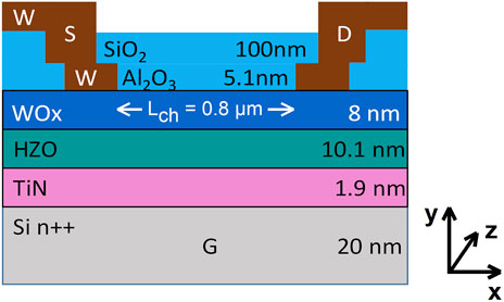
FIGURE 1. Epitaxial structure of the HZO-based, back-gated FeFET which serves as a calibration reference for this work (Halter et al., 2020). The ferroelectric HZO gate dielectric, the WOx channel, the source (S), the drain (D), and the gate (G) regions are indicated. The thickness of all layers and the channel length are given in nanometers and micrometers, respectively. Note that only 2-D structure is used during simulations.
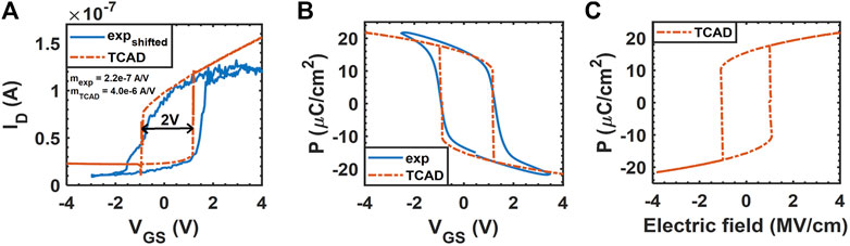
FIGURE 2. Experimental (solid blue line) and simulation (dash-dotted red line) DC characteristics for the FeFET in Figure 1 with an 8 nm-thick WOx channel (Halter et al., 2020). (A) “Drain current ID vs. gate voltage VGS” hysteresis at VDS = 0.2 V; (B) “Polarization vs. gate voltage” data; (C) “Polarization vs. electric field” characteristics of the ferroelectric HZO layer. Only simulation results are available for this quantity.
The ferroelectric model relies on several material parameters, in particular the Landau coefficients αi, βi, and γi. The default parameters that are available in the S-Device library have been utilized as initial values. They have then been slightly adjusted to best match capacitance measurements. Consequently, the sole uncertainty in the calibration of the FeFET simulation model resides in the material parameters for WOx. To obtain them, we used the experimental WOx data presented in (Migas et al., 2010; Halter et al., 2020) and the values proposed in (Fountaine, 2015) for WO3. The most relevant material parameters for HZO and WOx that were employed in our simulations are shown in Tables 1, 2. Note that since 2-D simulations are carried out in this study, all coefficients along the z-axis of the HZO layer are defined to be zero. The Landau coefficients αi, βi, and γi in the first five rows of Table 1 determine the polarization component Pi along the axis i = {x, y, z}, in case of anisotropic dielectric layer. Similarly, the gij coefficients refer to the polarization gradient factor that influences the spatial derivative of Pi (Eq. 1). The polarization is assumed to be anisotropic to restrict the switchable component to the y-axis, which is the direction orthogonal to the gate of the transistor, whose structure is schematized in Figure 1. This feature is realized by defining positive αi values along the two other directions, i.e., the x- and z-axis. Generally, the polarization gradient coefficients gij is a symmetric 3 × 3 tensor, which has six independent components. It can therefore be expressed in a six-component vector notation: g1 = g11, g2 = g22, g3 = g33, g4 = g23 = g32, g5 = g13 = g31, and g6 = g12 = g21 (Synopsys, 2019). Regarding the relative permittivity of WOx, a value higher (

TABLE 1. Principle S-Device material parameters for the considered HZO ferroelectric layer.
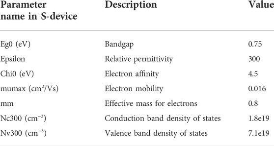
TABLE 2. Same as in Table 1, but for the WOx channel.
The simulated and experimental characteristics of the 2-D FeFET structure are shown in Figure 2. In sub-plot (A), the experimental “ID vs. VGS” hysteretic loop is presented. The measured curve was shifted along the positive VGS direction by 1 V, as compared to the simulation data, to compensate for the accumulation of trapped charges, an effect that is not accounted for in our model (Muller et al., 2016). Apart from this rigid shift that must be applied, a good agreement between the calibrated TCAD results and the measured data can be observed. The simulated hysteretic window is about 2 V wide, similar to the experimental one. The flatter dID/dVGS slope of the experimental measurement can be attributed to the formation of a high density of ferroelectric domains inside the HZO layer, as will be discussed in Section 3.2. In addition, the simulated and experimental “polarization vs. gate voltage (P vs. VGS)” characteristics of the ferroelectric HZO layer agree very well, as shown in sub-plot (B). In sub-plot (C), the “polarization vs. electric field” behavior of the HZO layer, as computed with the TCAD model, is presented. No experimental data is available for this quantity.
3.2 Multi-domain characterization
Based on this initial calibration, the agreement between the simulated and measured characteristics of the selected FeFET have been further improved by accounting for the presence of multiple ferroelectric domains. As the number of domains increases in the HZO layer, the dID/dVGS slope of the switching hysteresis and the value of the ferroelectric coercive field (EC) change, as compared to the single-domain case that has been so far assumed. When the required electric field and time for the polarization to switch are different in each ferroelectric domain, the slope of the electrical current ID with respect to the gate voltage VGS becomes more gradual, for both branches of the hysteresis. This indicates that polarization switching takes place in a sequential manner across all grains (Noh et al., 2019).
To include this effect, the ferroelectric HZO layer in the modeled FeFET structure was divided into ND domains with equal size LD along the x-axis. These domains join the source and drain contacts possess varying Landau’s coefficients α2n along the y-axis, since α2n is closely related to the remnant polarization Pr and the coercive field EC of the concerned domain, according to Eqs 1, 2. Here, the subscript of the Landau coefficient n corresponds to the index of the ferroelectric domain along y, n = 1 being the first one on the source side, and n = ND the last one close to the drain contact. The α2n values were randomly chosen according to a Gaussian distribution function with a mean value μα2 = −9.889 × 1010 cm/F and standard deviations σα2 varying between 0 and 9.889 × 1010 cm/F.
The simulated “ID vs. VGS” characteristics of four different HZO domain configurations (ND and LD) are plotted in Figures 3A–D, together with the experimental reference. Note that the product ND × LD remains the same in all cases, 0.8 μm, which is equal to the total length of the WOx channel. It can be clearly observed that the slope of the hysteresis loop decreases when increasing σα2. Among all tested configurations, the one with ND = 40, LD = 20 nm, and σα2 = −0.3μα2 in Figure 3C gives the best agreement with the measurement. Moreover, the simulation with ND = 80, LD = 10 nm, and σα2 = −0.3μα2 leads to a similar result, but with slightly larger discrepancy. Since the domain size is generally smaller than the grain size (Hyun et al., 2018), this finding aligns well with the experimental observation of a mean grain size in HZO of 26.8 nm, as reported in (Lombardo et al., 2021).
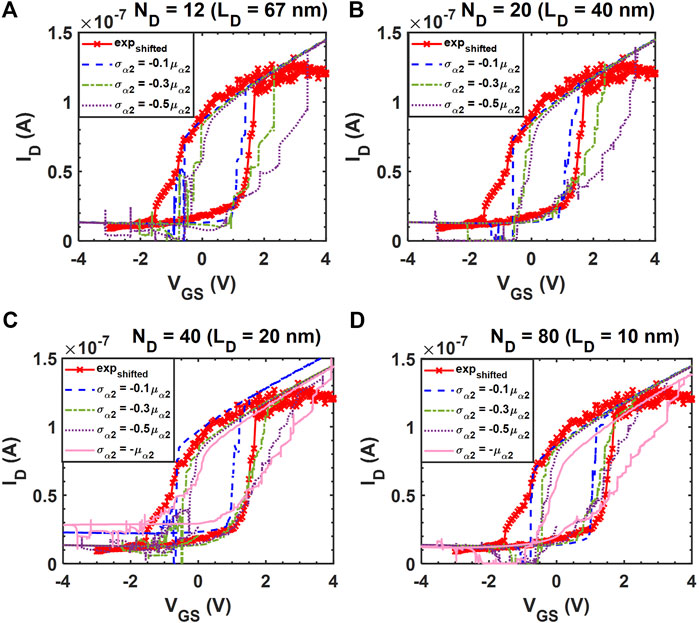
FIGURE 3. Experimental (solid line with crosses) and simulated “ID vs. VGS” transfer characteristics of the FeFET in Figure 1 with an 8 nm-thick WOx channel (Halter et al., 2020), different number of HZO domains (ND), and varying standard deviations of the Landau coefficients (σα2) at a source-to-drain voltage VDS = 0.2 V (A) ND = 12, LD = 67 nm; (B) ND = 20, LD = 40 nm; (C) ND = 40, LD = 20 nm; (D) ND = 80, LD = 10 nm.
Next, we focused on the transient response of the WOx-based FeFET to a train of positive and negative electrical pulses applied to its source and drain contacts, while the gate is grounded. Desired is a gradual, multi-state modulation of the device resistance as a function of the number of applied pulses. As a first numerical analysis, the influence of ND on the number of resistance states was investigated at a constant standard deviation value of σα2 = −0.3μα2. Results are shown in Figure 4. The amplitude of the electrical pulses first increases from 0 to 4 V in step of 0.1 V before decreasing from 0 to −4 V with a step size of −0.1 V. As a consequence, the resistance first increases (depression) and then decreases (potentiation). The duration of the writing pulses is set to 10 µs, as in experiments (Halter et al., 2020). As expected, the number of available resistance states increases as more ferroelectric domains ND are considered. The maximum number of resistance states (15) is reached with ND = 40 and 80, which corresponds to domain sizes of 20 and 10 nm, respectively, the length of the channel still being equal to 0.8 μm.
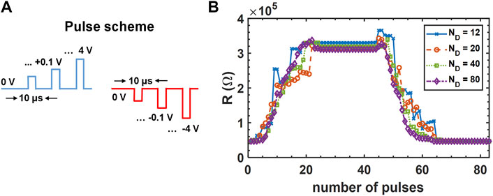
FIGURE 4. Simulated response of the WOx-based FeFET of Figure 1 to a train of electrical pulses (as shown in subplot (A)) applied to the drain and source electrodes, while the gate is grounded. The pulse amplitude increases from 0 to 4 V and then decreases from 0 to −4 V, with a step size of ±0.1 V and a period of 10 μs. Different number of domains ND (from 12 to 80) at a constant standard deviation σα2 = −0.3μα2 are considered.
Continuing our analysis, the potentiation and depression behavior of the WOx-based FeFET is investigated for LD = 10 and 20 nm with varying σα2. Here, the same electrical pulse sequence as in the measurements is used (Halter et al., 2020). Their amplitude increases first from 1.3 to 2.7 V for depression and then decreases from −1.5 to -2.5 V for potentiation, with a step size of ±0.1 V and a pulse duration of 10 μs. The simulated results are summarized and compared to experiments in Figure 5. For σα2 ≤ −0.5 μα2, the difference in RH/RL obtained at the two ND considered here comes from the fact that the ferroelectric domains are not fully switched due to the relatively limited voltage swing of the applied pulses (from 1.3 to 2.7 V for depression and from −1.5 to −2.5 V for potentiation). The best agreement is obtained when ND = 40, LD = 20 nm, and σα2 = −μα2. These results can then be used to extract the RH/RL resistance ratio, where RH (RL) refers to the largest (smallest) resistance occurring in the depression/potentiation curve in Figure 5. This ratio is found to be 1.6. It should be noticed that the best match between the measured and simulated depression and potentiation characteristics is obtained for a larger standard deviation σα2 than in the optimal DC case in Figure 3C. In Figure 3C, σα2 = μα2 produces a good agreement with the experimental “ID vs. VGS” curve. This discrepancy could possibly be attributed to the fact that for durations longer than 3 µs, the energy of each pulse is potentially large enough to enable oxygen migration between the HZO and WOx layers, which increases the RH/RL resistance ratio as compared to the case where only polarization switching occurs (Halter et al., 2022). As the migration of oxygen atoms cannot be described by the current TCAD model, the discrepancy between the quasistatic and transient results corresponds to the difference between the calibrated standard deviations of Landau’s coefficients. In addition, larger RH/RL are expected for pulse durations longer than 10 µs, as confirmed experimentally (Halter et al., 2022). Note that the orientation of the polarization is restricted to the y-axis in this study although the switching characteristics of the investigated devices closely relies on this parameter and its variation across the multiple ferroelectric domains. This partly explains the differences between simulations and experiments.
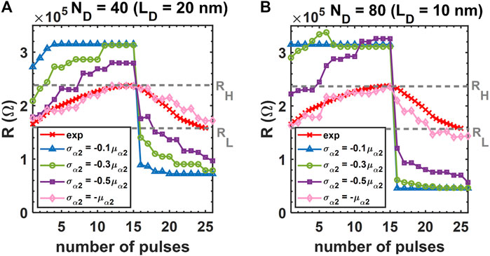
FIGURE 5. Simulated and experimental depression and potentiation response of the WOx-based FeFET of Figure 1 as a function of the number of electrical pulses at different standard deviations σα2 for (A) ND = 40, LD = 20 nm; (B) ND = 80, LD = 10 nm domain configurations. The writing pulse train increases from 1.3 to 2.7 V for depression and then decreases from −1.5 to −2.5 V for potentiation, with a step size of ±0.1 V. The experimental RH and RL values are both indicated. They correspond to the resistance at the beginning of the pulse sequence (RL) and at the end of the depression part (RH).
4 Prospective performance enhancements
Starting from the calibrated simulation results of Section 3, the influence of various design parameters has been studied to enhance the FeFET performance. More specifically, our theoretical investigations aim at designing novel FeFET structures with improved RH/RL resistance ratios, i.e., with larger dynamic ranges, as compared to the device configuration reported in (Halter et al., 2020). The higher the RH/RL ratio, the more efficient is the training of a crossbar array incorporating such devices. If possible, the number of available resistance states between RL and RH should also be maximized. All channel resistances are extracted at VDS = 0.2 V by applying a DC IV-sweep from −200 to 200 mV at the drain contact, while keeping the source and the gate grounded, as in experiments (Halter et al., 2020). For simplicity, all subsequent simulations were carried out utilizing FeFETs with a single-domain HZO layer, as the number of ferroelectric domains is not expected to significantly affect the resistance ratio of the device, as can be seen in Figure 4.
Because pulse-response simulations are computationally relatively intensive, the resistance ratios of the modified device designs were estimated as a first approximation by scaling the RH/RL results in Figure 5 with the following factor:
4.1 Impact of design parameters
4.1.1 Channel thickness
As a first design parameter, the impact of the channel thickness, TCH, was analyzed taking advantage of the calibrated model. The simulation results are displayed in Figure 6. It can be observed in sub-plot (A) that by decreasing TCH from 8 to 4 nm, the RH/RL ratio, as estimated with the method outlined above, doubles. This finding has been confirmed experimentally, where an improvement by a factor 2 is obtained by halving the channel thickness of the FeFET (Halter et al., 2022). These results are not only encouraging, they also validate our approach, where only the DC FeFET characteristics are computed to approximate the RH/RL ratio. For TCH thicker than 10 nm, the estimated RH/RL ratio drops to unity due to the relatively low energy barrier between the source and drain regions, which leads to a decreased ION/IOFF.
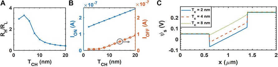
FIGURE 6. (A) RH/RL resistance ratio as a function of the channel thickness TCH, estimated from the hysteretic FeFET characteristics at VDS = 0.2 V. (B) Corresponding ION and IOFF as a function of TCH, extracted from the DC transfer characteristics at 4 V and −4 V, respectively. (C) Surface potential ψS along the WOx channel at VG = −4 V and VDS = 0.2 V. The beginning of the source contact is situated at x = 0, the gate starts at x = 0.6 μm and goes till x = 1.4 μm.
It can be seen in subplot (B) and that the increase in RH/RL can be mainly attributed to a rapid decrease of IOFF as TCH is reduced before saturating. The ON-state current also diminishes, but at a slower rate. This behavior is a consequence of the fact that transistors with a thinner channel exhibit a better electrostatics control than thicker ones, thus allowing for a more efficient switching off of the device. Further reducing TCH below 4 nm does not bring additional enhancement anymore because IOFF remains almost constant. At this size, IOFF is limited by the electron carrier concentration of the channel, which is equal to 1.01 × 1020 cm−3 in our case (Si et al., 2019). Moreover, the surface potential at the source/channel interface is already negative at TCH = 4 nm, as can be seem in Figure 6C. It thus forms a potential barrier at the source-gate interface so that further reductions of TCH have little impact on IOFF. In conclusion, an enhanced RH/RL ratio can be achieved by carefully adjusting TCH.
4.1.2 HZO thickness
The transfer characteristics of the FeFET device have also been evaluated for different HZO layer thicknesses, TFE. As shown in Figure 7, the RH/RL ratio increases as TFE decreases. The underlying physical mechanism is similar to the one discussed in Section 4.1.1, i.e., the gate control over the channel becomes stronger as the ferroelectric layer thickness is reduced because the gate capacitance augments. The impact of TFE is stronger on ION than on IOFF, which leads to the observed positive effect on RH/RL. According to our simulations, if TFE is reduced down to 5 nm, a further increase of RH/RL could theoretically be envisioned, but two major issues might prevent such a positive outcome. First, thin HZO layers are known not to switch as efficiently as thicker ones (Vitale et al., 2010). Secondly, an ultra-scaled dielectric layer tends to be leaky and to induce large gate leakage currents. Note also that the benefit of thinning the HZO layer is less important than a reduction of the semiconductor channel thickness. It is therefore not the preferred option.
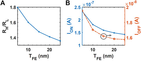
FIGURE 7. (A) Simulated RH/RL resistance ratio as a function of the ferroelectric layer thickness TFE. (B) Corresponding ION and IOFF currents as a function of TFE. All simulations were performed at VDS = 0.2 V.
4.1.3 Gate length, channel width, and source/drain extensions
Contrary to the two previous parameters, TCH and TFE, which directly affect the depression and potentiation behavior of WOx-based FeFETs, the lateral dimensions of the structure, the gate length LG, and the source/drain extensions LS/D, have little influence on the RH/RL ratio. The ON- and OFF-state currents scale proportionally to “1/LCH”, so that their impact on the RH/RL ratio cancels each other (KO, 1989). On the other hand, it has been observed that the length of the source/drain contact extensions, LS/D, has a negligible influence on the simulated RH/RL ratios of the FeFETs.
4.2 Double-gate architecture
Based on our simulation results as well as on experimental evidence, regardless of the device dimensions and channel doping concentrations (not shown here), it clearly appears that the originally proposed back-gated (BG) FeFET structure with a WOx channel cannot deliver RH/RL resistance ratios larger than ∼4. As a consequence, to improve the performance, a different transistor design is required. Here, we propose a symmetric, double-gate (DG), WOx-based FeFET with a planar structure, as schematized in Figure 8. Its geometrical parameters are summarized in Table 3. Its dimensions are similar to those of the original BG FeFET, but with two instead of one gate contact and a length of the HZO ferroelectric layer that does not exceed that of the gates. In other words, the source and drain extensions are not covered by HZO.
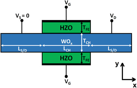
FIGURE 8. Simulated double-gate FeFET structure with a planar WOx channel. Its dimensions are listed in Table 3.
TABLE 3. Geometrical parameters of the double-gate FeFET transistor in Figure 8.
The transfer characteristics of the proposed FeFET design are reported in Figure 9 and compared to those of the original back-gated FeFET of Figure 1. With the same dimensions in both transistor configurations, the introduction of a second gate significantly improves the electrostatic control, which helps suppress the OFF-state current, while slightly improving the ON-state current by a factor of 1.6, as compared to the original structure. Hence, the DG device with an 8 nm WOx channel and a 10 nm HZO layer could theoretically deliver a 13 times higher RH/RL resistance ratio than the original one with a single back gate, i.e., 20.8 instead of 1.6. This improvement is expected to be accompanied by a significant increase of the number of intermediate resistance states between RL and RH. Obviously, reducing the WOx channel thickness could further enhance the RH/RL ratio, but not as much as in the back-gated FeFET because the electrostatic control is already close to optimal with a double-gate architecture and TCH = 8 nm.
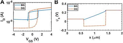
FIGURE 9. (A) Simulated transfer characteristics “ID-VGS” of the double-gate FeFET of Figure 8 and of the original back-gated FeFET of Figure 1. (B) Extracted surface potential ψS along the channel at VGS = -4 V and VDS = 0.2 V.
5 Conclusion
The transfer characteristics of HZO-based FeFETs were simulated utilizing a 2-D, time-depedent Ginzburg-Landau ferroelectric model, as implemented in the S-Device TCAD tool. Starting from an existing back-gated FeFET with a WOx channel, good qualitative and quantitative agreements between the simulated and experimental DC performance were obtained after careful calibration. The influence of different design parameters (channel and ferroelectric layer thickness, gate length) and device geometries (double-gate architecture) on the RH/RL resistance ratio of these transistors were investigated. This ratio is a relevant figure-of-merit for neuromorphic computing applications because it is closely related to the dynamic range of the depression and potentiation characteristics and to the number of available resistance states that can be accessed by sending electrical pulses to the FeFETs. The RH/RL ratio should be as large as possible to enhance the learning capabilities of artificial neural networks based on memristive FeFET crossbar arrays. In terms of parameter screening, a channel thickness of 4 nm seems to be optimal, regardless of the device geometry. It should be combined with a ferroelectric layer as thin as possible, while maintaining good polarization switching properties and low leakage currents.
However, to avoid large surface-to-volume ratios and minimize the impact of surface roughness, as typically encountered in ultra-thin channels, a double-gate FeFET appears as a more promising approach. It provides the best electrostatic control over the WOx channel, and is predicted to provide a 13 times larger RH/RL ratio than that of the original back-gated transistor with similar geometrical parameters. From a fabrication point of view, a double-gate structure might be more challenging than a reduction of the channel or ferroelectric layer thickness, but the benefit is far greater. Hence, the HZO-based FeFET technology might be a viable alternative to phase change materials, valence change memories, or electro-chemical cells as solid-state synapses in future neuromorphic computing circuits.
Data availability statement
The raw data supporting the conclusion of this article will be made available by the authors, without undue reservation.
Author contributions
XW and ML led the project. XW carried out the simulations. MH and LB-L designed and performed the experiments. XW and ML wrote and edited the paper. All authors contributed to the article and approved the submitted version.
Funding
This work was supported by the EU H2020 ICT BeFerroSynaptic project No. 871737. Open access funding provided by ETH Zurich.
Acknowledgments
We acknowledge Pawel Lenarczyk for the implementation of the simulation model and the helpful theoretical and technical support.
Conflict of interest
MH and LB-L are employed by IBM Research GmbH—Zurich Research Laboratory.
The remaining authors declare that the research was conducted in the absence of any commercial or financial relationships that could be construed as a potential conflict of interest.
Publisher’s note
All claims expressed in this article are solely those of the authors and do not necessarily represent those of their affiliated organizations, or those of the publisher, the editors and the reviewers. Any product that may be evaluated in this article, or claim that may be made by its manufacturer, is not guaranteed or endorsed by the publisher.
References
Ali, T., Polakowski, P., Riedel, S., Büttner, T., Kämpfe, T., Rudolph, M., et al. (2018). Silicon doped hafnium oxide (hso) and hafnium zirconium oxide (hzo) based fefet: A material relation to device physics. Appl. Phys. Lett. 112, 222903. doi:10.1063/1.5029324
Apalkov, D., Khvalkovskiy, A., Watts, S., Nikitin, V., Tang, X., Lottis, D., et al. (2013). Spin-transfer torque magnetic random access memory (stt-mram). ACM J. Emerg. Technol. Comput. Syst. (JETC) 9, 1–35.
Chandra, P., and Littlewood, P. (2007). “A landau primer for ferroelectrics,” in Physics of ferroelectrics (Berlin, Heidelberg: Springer), 69–116. doi:10.1007/978-3-540-34591-6_3
Chen, C., Yang, M., Liu, S., Liu, T., Zhu, K., Zhao, Y., et al. (2019). “Bio-inspired neurons based on novel leaky-fefet with ultra-low hardware cost and advanced functionality for all-ferroelectric neural network,” in 2019 symposium on VLSI technology (IEEE), T136–T137. doi:10.23919/VLSIT.2019.8776495
Cockburn, B., Kanschat, G., Schötzau, D., and Schwab, C. (2002). Local discontinuous galerkin methods for the Stokes system. SIAM J. Numer. Analysis 40, 319–343. doi:10.1137/S0036142900380121
Fountaine, K. T. (2015). Mesoscale optoelectronic design of wire-based photovoltaic and photoelectrochemical devices. Pasadena, California: California Institute of Technology. PhD Thesis.
Gokmen, T., and Vlasov, Y. (2016). Acceleration of deep neural network training with resistive cross-point devices: Design considerations. Front. Neurosci. 10, 1. doi:10.3389/fnins.2016.00333
Halter, M., Bégon-Lours, L., Bragaglia, V., Sousa, M., Offrein, B., Abel, S., et al. (2020). A back-end, cmos compatible ferroelectric field effect transistor for synaptic weights. ACS Appl. Mat. Interfaces 12, 17725–17732. doi:10.1021/acsami.0c00877
Halter, M., Bégon-Lours, L., Sousa, M., Popoff, Y., Drechsler, U., Bragaglia, V., et al. (2022). A multi-timescale synaptic weight based on ferroelectric hafnium zirconium oxide. Springer. (to be submitted).
Hyun, S. D., Park, H. W., Kim, Y. J., Park, M. H., Lee, Y. H., Kim, H. J., et al. (2018). Dispersion in ferroelectric switching performance of polycrystalline hf0.5zr0.5o2 thin films. ACS Appl. Mater. Interfaces 10, 35374–35384.
Jerry, M., Chen, P.-Y., Zhang, J., Sharma, P., Ni, K., Yu, S., et al. (2017). “Ferroelectric fet analog synapse for acceleration of deep neural network training,” in 2017 IEEE international electron devices meeting (IEDM) (IEEE), 6.2.1–6.2.4. doi:10.1109/IEDM.2017.8268338
Ko, P. K. (1989). “Chapter 1 - approaches to scaling,” in Advanced MOS device physics, vol. 18 of VLSI electronics microstructure science. Editors N. G. Einspruch, and G. S. Gildenblat (Elsevier), 1–37. doi:10.1016/B978-0-12-234118-2.50005-X
Lombardo, S. F., Tian, M., Chae, K., Hur, J., Tasneem, N., Yu, S., et al. (2021). Local epitaxial-like templating effects and grain size distribution in atomic layer deposited hf0.5zr0.5o2 thin film ferroelectric capacitors. Appl. Phys. Lett. 119, 092901. doi:10.1063/5.0057782
Migas, D. B., Shaposhnikov, V. L., and Borisenko, V. E. (2010). Tungsten oxides. ii. the metallic nature of magneli phases. J. Appl. Phys. 108, 093714. doi:10.1063/1.3505689
Mulaosmanovic, H., Chicca, E., Bertele, M., Mikolajick, T., and Slesazeck, S. (2018). Mimicking biological neurons with a nanoscale ferroelectric transistor. Nanoscale 10, 21755–21763.
Mulaosmanovic, H., Ocker, J., Müller, S., Noack, M., Müller, J., Polakowski, P., et al. (2017). “Novel ferroelectric fet based synapse for neuromorphic systems,” in 2017 symposium on VLSI technology (IEEE), T176–T177. doi:10.23919/VLSIT.2017.7998165
Mulaosmanovic, H., Slesazeck, S., Ocker, J., Pesic, M., Muller, S., Flachowsky, S., et al. (2015). “Evidence of single domain switching in hafnium oxide based fefets: Enabler for multi-level fefet memory cells,” in 2015 IEEE international electron devices meeting (IEDM) (IEEE), 26.8.1–26.8.3. doi:10.1109/IEDM.2015.7409777
Muller, J., Polakowski, P., Muller, S., Mulaosmanovic, H., Ocker, J., Mikolajick, T., et al. (2016). “High endurance strategies for hafnium oxide based ferroelectric field effect transistor,” in 2016 16th non-volatile memory technology symposium (NVMTS) (IEEE), 1–7. doi:10.1109/NVMTS.2016.7781517
Noh, Y., Jung, M., Yoon, J., Hong, S., Park, S., Kang, B. S., et al. (2019). Switching dynamics and modeling of multi-domain zr-doped hfo2 ferroelectric thin films. Curr. Appl. Phys. 19, 486–490. doi:10.1016/j.cap.2019.01.022
Selberherr, S. (1984). Analysis and simulation of semiconductor devices. Springer Science & Business Media.
Sholl, D., and Steckel, J. A. (2011). Density functional theory: A practical introduction. John Wiley & Sons.
Si, M., Lyu, X., Shrestha, P. R., Sun, X., Wang, H., Cheung, K. P., et al. (2019). Ultrafast measurements of polarization switching dynamics on ferroelectric and anti-ferroelectric hafnium zirconium oxide. Appl. Phys. Lett. 115, 072107. doi:10.1063/1.5098786
Starkov, A., Pakhomov, O., and Starkov, I. (2013). Theoretical model for thin ferroelectric films and the multilayer structures based on them. J. Exp. Theor. Phys. 116, 987–994. doi:10.1134/S1063776113060149
Sun, X., Wang, P., Ni, K., Datta, S., and Yu, S. (2018). “Exploiting hybrid precision for training and inference: A 2t-1fefet based analog synaptic weight cell,” in 2018 IEEE international electron devices meeting (IEDM) (IEEE), 3.1.1–3.1.4. doi:10.1109/IEDM.2018.8614611
Vitale, W., Mohamed, M., and Ravaioli, U. (2010). “Monte Carlo study of transport properties in junctionless transistors,” in 2010 14th international workshop on computational electronics (IEEE), 1–3. doi:10.1109/IWCE.2010.5677969
Zhao, W., Devolder, T., Lakys, Y., Klein, J., Chappert, C., and Mazoyer, P. (2011). Design considerations and strategies for high-reliable stt-mram. Microelectron. Reliab. 51, 1454–1458. doi:10.1016/j.microrel.2011.07.001
Keywords: HZO, FeFET, TCAD, ferroelectric modeling, device simulation
Citation: Wen X, Halter M, Bégon-Lours L and Luisier M (2022) Physical modeling of HZO-based ferroelectric field-effect transistors with a WOx channel. Front. Nanotechnol. 4:900592. doi: 10.3389/fnano.2022.900592
Received: 20 March 2022; Accepted: 19 July 2022;
Published: 25 August 2022.
Edited by:
Patrick D. Lomenzo, NaMLab gGmbH, GermanyReviewed by:
Amey Walke, Interuniversity Microelectronics Centre (IMEC), BelgiumMaximilian Lederer, Fraunhofer Institute for Photonic Microsystems, Germany
Copyright © 2022 Wen, Halter, Bégon-Lours and Luisier. This is an open-access article distributed under the terms of the Creative Commons Attribution License (CC BY). The use, distribution or reproduction in other forums is permitted, provided the original author(s) and the copyright owner(s) are credited and that the original publication in this journal is cited, in accordance with accepted academic practice. No use, distribution or reproduction is permitted which does not comply with these terms.
*Correspondence: Xin Wen, d2VueEBpaXMuZWUuZXRoei5jaA==