- 1Department of Frontier Materials, Nagoya Institute of Technology, Nagoya, Japan
- 2Graduate School of Engineering, Nagoya University, Nagoya, Japan
- 3UVSOR Facility, Institute for Molecular Science, Okazaki, Japan
- 4School of Physical Sciences, The Graduate University for Advanced Studies (SOKENDAI), Okazaki, Japan
- 5Graduate School of Frontier Biosciences and Department of Physics, Graduate School of Science, Osaka University, Suita, Japan
The electronic structure of single-crystalline EuO (100) ultrathin films, together with their exchange splitting energy (ΔEEX) and ferromagnetic phase transition temperature (TC), was investigated by temperature- and thickness-dependent angle-resolved photoemission spectroscopy. Both ΔEEX and TC decreased monotonically with decreasing film thickness. The band shift showed an opposite thickness dependence at the Γ and X points, reflecting the balance of the hybridization between the Eu 4f and O 2p states (super-exchange interaction) and between the Eu 4f, O 2p, and Eu 5d states (indirect-exchange interaction). The observed transition from an indirect energy gap in the bulk to a direct gap in the ultrathin films of the ferromagnetic semiconductor EuO could be potential in future spintronic devices.
Introduction
Europium monochalcogenides (EuX; X = O, S, Se, and Te) are known as ideal Heisenberg ferromagnets exhibiting a high magnetic moment originating from localized Eu2+ 4f states and a large exchange splitting energy (ΔEEX) of the Eu 5 conduction state below the Curie temperature (TC) (Mauger and Godart, 1986). In particular, EuO has shown the highest TC (about 70 K), the largest ΔEEX, and the lowest work function of all these compounds (Eastman et al., 1969; Mauger and Godart, 1986). Because of recent observations of fully polarized electrons in electron-doped EuO and an increase of TC to about 200 K upon La doping (Steeneken et al., 2002; Schmehl et al., 2007; Miyazaki et al., 2010), EuO has attracted considerable attention for the development of next-generation spintronics applications, such as spin injectors and spin-polarized photocathodes. However, EuO is an indirect energy gap ferromagnetic semiconductor that shows the lowest energy transition from the valence to conduction bands which involves a change in wave vector. This typically creates inefficient and complicated events in interband transitions, making these materials unsuitable for spintronics applications (Zhang et al., 2001).
The use of ferromagnetic semiconductors in spintronics devices depends on reduction of their thickness to a few atomic layers by creating low-dimensional magnetic ultrathin films and controlling their electronic band structure by changing their indirect energy gap into their indirect counterpart. A thickness-dependent calculation of the electronic structure of EuO thin films (Schiller, Müller, and Nolting) has shown that TC and ΔEEX decreased with decreasing thickness. Experimental TC values were qualitatively consistent with theoretical predictions for ultrathin films with several atomic layers (Santos and Moodera, 2004; Müller et al., 2009; Negusse et al., 2009). However, the thickness-dependent ΔEEX and detailed band structure have not been investigated experimentally despite their great importance in the design of spintronics devices. The ΔEEX value in the EuO ultrathin films of fixed thickness has been determined using the Andreev reflection (Schmehl et al., 2007) and spin-resolved soft X-ray absorption measurements (Steeneken et al., 2002). These studies indicate that ultrathin films exhibit a smaller ΔEEX than bulk films, consistent with the theoretical predictions.
Three-dimensional angle-resolved photoemission spectroscopy (3D-ARPES) studies have pointed out that ΔEEX appears in the energy shift of Eu 4f bands, and the indirect band gap forms according to the theoretically predicted band structures (Miyazaki et al., 2009; Miyazaki et al., 2013). Thickness-dependent 3D-ARPES is expected to provide information about the thickness-dependent TC, ΔEEX, and detailed electronic band structure changes occurring with decreasing thickness. Therefore, in order to obtain information on the detailed electronic structure and magnetic properties, such as the TC and ΔEEX, we performed the thickness- and temperature-dependent 3D-ARPES measurements for EuO ultrathin films with various thicknesses.
Experimental and Theoretical Procedures
Single-crystalline 2–8 and 20-nm EuO (100) ultrathin films were grown using a molecular beam epitaxy method. To grow high-quality ultrathin films, a 5-nm SrO thin film acting as a buffer layer was deposited between the EuO ultrathin films and SrTiO3 substrate (Figure 1A) because SrO forms a rock-salt type crystal structure with a lattice constant of 0.5144 nm, similar to EuO (the lattice mismatch between SrO and EuO is 0.3%) (Miyazaki et al., 2012). The substrates were heated at 600°C for 1 h under an ultrahigh vacuum (2.0−7 Pa × 10−7 Pa) to clean their surfaces. The SrO buffer layer and EuO ultrathin films were grown by the sequential evaporations of Sr and Eu metals under oxygen pressures of 1.0 × 10⁻⁴ and 8.0−6 Pa × 10−6 Pa, respectively, at a substrate temperature of 400°C.
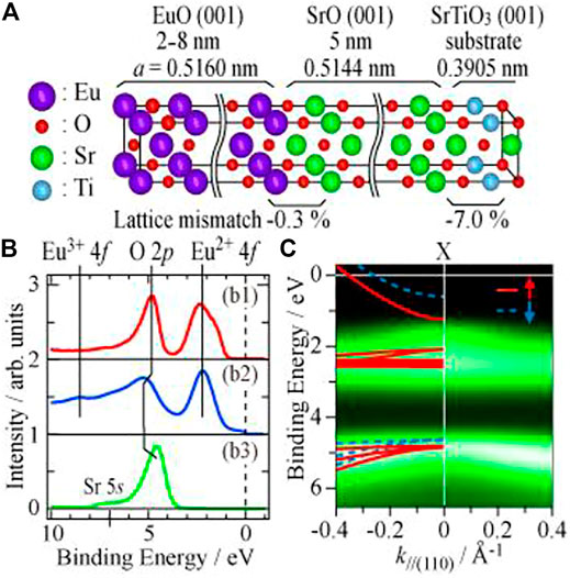
FIGURE 1. (A) Atomic structure of a EuO (100) thin film deposited with a SrO buffer layer on a SrTiO3 substrate. Lattice constants and mismatch are provided. (B) PES spectra of 2-nm EuO/5-nm SrO/SrTiO3 (b1), 5-nm EuO/SrTiO3 (b2), and 5-nm SrO/SrTiO3 (b3) at 10 K (hν = 38 eV). (C) Comparison between an ARPES image of a 2-nm EuO (100) ultrathin film at 10 K near the X point and band calculation result.
Three-dimensional ARPES measurements along the surface normal were performed at the beamline 5U of the UVSOR-III synchrotron radiation facility at the Institute for Molecular Science (Ito et al., 2007). Γ and X points in the normal emission geometry corresponded to photon energies hν of 78 and 38 eV, respectively (Miyazaki et al., 2013). Total energy and momentum resolutions were set to 123 meV (45 meV) and 0.020 Å−1 (0.014 Å−1) at Γ (X) point, respectively. There is no significant change in the photoelectron spectrum due to the difference in energy resolution between the Γ and X points. Temperature-dependent 3D-ARPES spectra were recorded during the temperature decrease.
The electronic structure of EuO was calculated by a local spin density approximation plus Coulomb repulsion U (LSDA + U) using the Wien2k code (Blaha et al., 1990). The electron correlation energy U of the Eu 4f state was fixed at 7.0 eV (Ghosh et al., 2004). To calculate the electronic structure of EuO ultrathin films, we used the slab approach, in which periodic boundary conditions are applied to the surface supercell including a slab of atomic layers and a vacuum region as shown in Figures 2(a1) and 2 (a2).
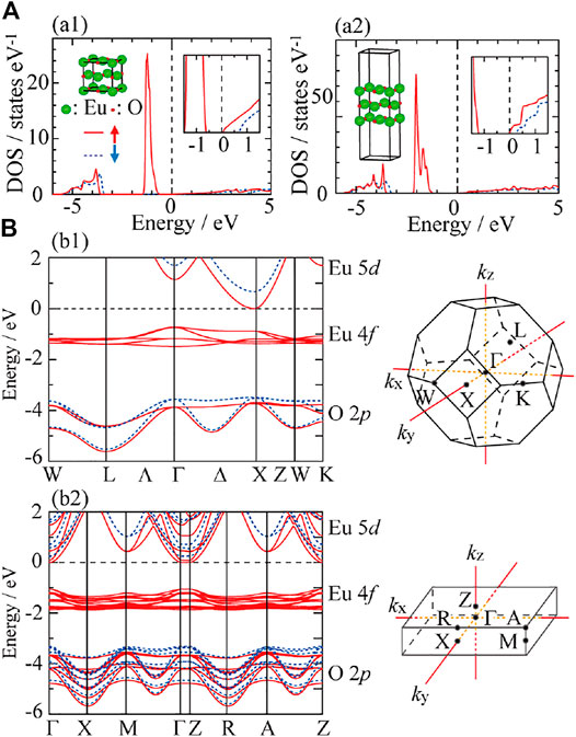
FIGURE 2. (A) Spin-dependent density of states (DOS) of bulk (a1) and 1-monolayer (a2) EuO calculated using the LSDA + U method. Insets show the modeled crystal structure and the DOS near EF. Spin-dependent band structure of the bulk (B) (b1) and 1-monolayer (b2) EuO.
Results and Discussion
To negate the existence of impurities, such as Eu2O3 and the Eu metal in the fabricated EuO ultrathin films, their compositions and the Eu valence were investigated by angle-integrated PES measurement. Figure 1B shows the PES spectra of 2 nm EuO/5 nm SrO/SrTiO3 [Figure 1B(1)], 5 nm EuO/SrTiO3 [Figure 1B(2)], and 5 nm SrO/SrTiO3 films [Figure 1B(3)] measured at 10 K for hν = 38 eV. The 2-nm EuO/5-nm SrO/SrTiO3 film only presented Eu2+ 4f and O 2p [Figure 1(b1)] although the 5-nm EuO/SrTiO3 displayed Eu3+ 4f and metallic states originating from Eu2O3 and Eu metal [Figure 1B(2)], respectively (Lee et al., 2007). These results suggest that the SrO buffer layer prevents oxygen diffusion from the SrTiO3 substrate to the EuO ultrathin film. The PES peaks attributable to the Sr 5s and O 2p states of the SrO buffer layer appeared at the same energy [Figure 1B(3)] as that of the O 2p state of EuO [Figure 1B(1)]. Because the O 2p state of EuO was indistinguishable from that of SrO, their corresponding spectra are not discussed in this study. Figure 1C shows an ARPES image of a 2-nm EuO ultrathin film at 10 K for hν = 38 eV, and the band structure of bulk EuO near the X point. A large dispersion curve was observed at the top of the Eu 4f state, consistent with the band calculation. This also agrees with previous results obtained for 50-nm EuO films (Miyazaki et al., 2009), implying that both EuO films exhibit equally high crystallinity. We succeeded in fabricating single-crystalline EuO ultrathin films with a continuously controlled few-atomic layer thickness.
Before reporting the detailed results of 3D-ARPES measurements, we show the expected electronic structure of EuO ultrathin film calculated using the LSDA + U method. Figures 2 (a1) and 2 (a2) show the spin-dependent density of states (DOS) of bulk and 1-monolayer EuO, respectively. The splitting energy between the minority and majority spin states of both Eu 5d and O 2p states decreases and the band gap increases in the thin-film limit. It indicates that the ΔEEX is decreasing from bulk to 1-monolayer EuO. Figures 2 (b1) and 2 (b2) show the spin-dependent band structure of bulk and 1-monolayer EuO, respectively. In the bulk EuO, the band structure shows the characteristics of a ferromagnetic semiconductor with an indirect band gap. On the other hand, in the 1-monolayer EuO, a direct band gap is realized. With decreasing thickness, the hybridization between the Γ and Z directions is expected to decrease. Since the strong hybridization between the constituent elements is the origin of the ferromagnetic phase in EuO, decreasing hybridization may cause a decrease in the TC and ΔEEX.
Temperature-dependent 3D-ARPES spectra were recorded for EuO ultrathin films with various thicknesses to determine the influence of film thickness on TC and ΔEEX. Figures 3A,B show the temperature-dependent energy distribution curves (EDCs) of the Eu 4f state in 8- and 2-nm EuO ultrathin films, respectively, at the X point. Because the X and Z points along the perpendicular line of the Brillouin zone, as shown in Figures 2(b1) and 2 (b2), were equivalent, we hereafter examine the X point. Peak and shoulder positions of the EDCs were evaluated from the local minima on the second-derivative EDCs. At the X point, EDCs consisted of two components. Based on previous band calculations (Miyazaki et al., 2009), higher and lower binding-energy components were attributed to the non-bonding and bonding Eu 4f states hybridized with the O 2p and Eu 5d states, respectively.
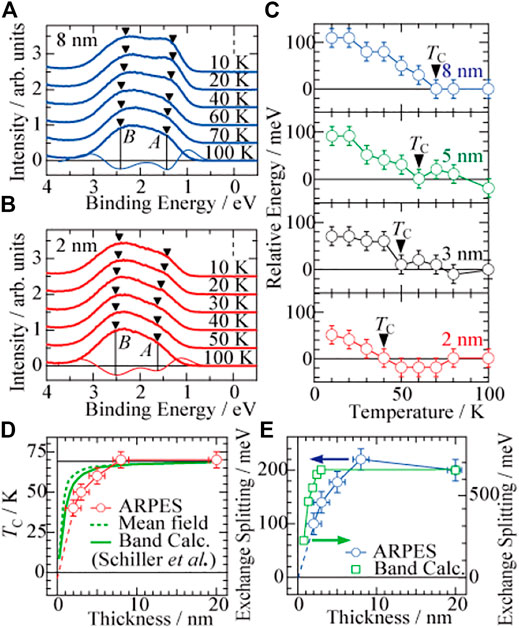
FIGURE 3. Temperature-dependent EDCs (thick solid lines) of the Eu 4f state in 8-nm (A) and 2-nm (B) EuO ultrathin films at the X point. Second-derivative curves (thin solid lines) at 100 K are also plotted. Vertical lines correspond to peaks in the second-derivative EDCs. The hybridized and non-bonding Eu 4f states are denoted by the letters A and B, respectively. (C) Temperature-dependent energy position of the non-bonding Eu 4f states (B) for thicknesses of 2, 3, 5, and 8 nm at the X point. TC was evaluated using the onset temperature. (D) Thickness-dependent TC evaluated from (C) and calculated by the mean field theory (Blaha et al., 1990) and a band calculation (Schiller, Müller, and Nolting). (E) Thickness-dependent ΔEEX evaluated from (C) and from a band calculation in Figures 2 (a1) and (a2).
The temperature-dependent energy shift of the non-bonding Eu 4f state stems from the exchange splitting of Eu 5d majority and minority bands during the ferromagnetic phase transition because the Fermi level (EF) is pinned at the bottom of the Eu 5d band at X point (Miyazaki et al., 2009). Because the exchange splitting occurred below TC, TC was determined using the temperature-dependent energy position of the non-bonding Eu 4f state. Figure 3C shows the temperature-dependent relative energy position of the non-bonding Eu 4f state at the X point in EuO ultrathin films for thicknesses of 2, 3, 5, and 8 nm. The onset temperature corresponds to TC as shown in Figure 3D. TC values calculated by the mean field theory (Jensen et al., 1992) and band calculation (Schiller, Müller, and Nolting) are also plotted as a function of temperature. TC gradually decreased with decreasing thickness, qualitatively consistent with previous experimental and theoretical results, (Santos and Moodera, 2004; Müller et al., 2009; Negusse et al., 2009), albeit with slightly lower TC values for films thinner than 5 nm.
The energy difference between the Eu 4f non-bonding state and the center of gravity of the Eu 5d majority and minority spin states must be constant across TC, and EF is located at the bottom of the Eu 5d majority band (Miyazaki et al., 2009). Consequently, the ΔEEX of the energy difference between these majority and minority spin states can be attributed to the doubling of the energy shift of the non-bonding Eu 4f state below TC. Figure 3E shows the thickness-dependent ΔEEX at 10 K derived from Figure 3C, along with the theoretical ΔEEX evaluated from band calculations in Figures 2 (a1) and 2 (a2). The experimental ΔEEX gradually decreased with decreasing thickness, exhibiting the same behavior as TC. At a thickness of 20 nm, the experimental ΔEEX was approximately one-third of the calculated value. On the other hand, the interpolated experimental ΔEEX amounted to one-tenth or less of the calculated value at 1 nm. Band calculations assumed a perfect hybridization and a crystal without interaction at its interface. Thus, this disagreement may originate from an overestimated hybridization and/or an underestimated interaction at its interface.
We now seek a reasonable explanation for the possible origin of the changing band structure in EuO ultrathin films leading to decreasing the thickness. Figure 4 shows the thickness-dependent EDCs of the Eu 4f state at Γ (a) and X (b) points in the ferromagnetic phase at 10 K. The hybridized Eu 4f state is denoted by the letter A, and non-bonding states are denoted by the letters B and B'. For the 8-nm EuO ultrathin film, the hybridized Eu 4f state at the Γ point was located at a lower binding energy side than that at the X point. Whereas for the 2-nm EuO ultrathin film, the hybridized Eu 4f state at the X point was observed at a lower binding energy side than that at the Γ point. Band calculations indicated that the bottom of the Eu 5d conduction band was located at the X point for EuO. Therefore, these results suggest that the electronic structure of EuO ultrathin film changes from indirect to direct energy gap at the X point when the thickness decreases. However, the previous band calculation results for 64-atom EuO thin films reported a direct energy gap (Monteiro et al., 2015), which is inconsistent with the present results. In the future, a systematic study of the band structure of EuO at various film thicknesses is needed to discuss the mechanism of the band gap change from direct to indirect with decreasing film thickness in more detail.
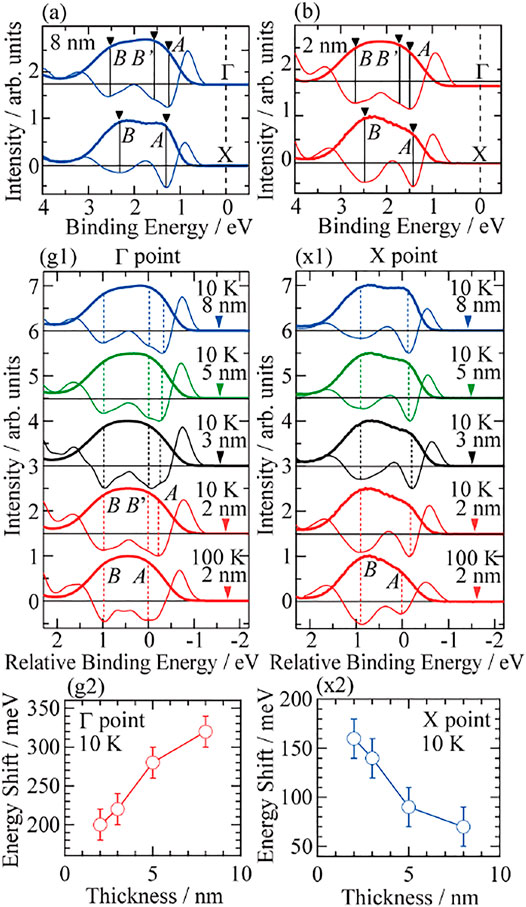
FIGURE 4. EDCs (thick lines) and corresponding second-derivatives (thin lines) of the Eu 4f state at the Γ (a) and X (b) points in the ferromagnetic phase at 10 K. Thickness dependence of the EDCs and their second-derivatives of EuO ultrathin films in the ferromagnetic phase (10 K) at the Γ (g1) and X (x1) points. EDCs in the paramagnetic phase (100 K) of the 2-nm EuO ultrathin film are also plotted. The hybridized Eu 4f state is denoted by the letter A, and non-bonding states are denoted by the letters B and B'. The zero relative binding energies in both (g1) and (x1) were set as the peak positions of A of 2-nm EuO ultrathin films at 100 K. The relative binding energy of B is fixed to the energy of that of 2-nm EuO ultrathin films at 100 K for other EDCs in (g1) and (x1). Triangles pointing downward represent EFs. The energy shift of A across TC is shown as a function of thickness at the Γ (g2) and X (x2) points.
To investigate the origin of the changes in the electronic structure with decreasing thickness, the zero relative binding energies in Figures 4 (g1) and 4 (x1) were set to the energy of peak A for the 2-nm EuO ultrathin film at 100 K at the Γ and X points, respectively. Because peak B corresponded to the non-bonding Eu 4f state (Miyazaki et al., 2009), the relative binding energies of peak B in the other EDCs were fixed to the energy of the 2-nm EuO ultrathin films at 100 K (1.0 and 0.9 eV at the Γ and X points, respectively). At the Γ point, as shown in Figure 4 (g1), peak A at 100 K split into two (A and B’) below TC for the 2-nm EuO ultrathin films. On the other hand, at the X point, as shown in Figure 4 (x1), shoulder A only shifted toward the lower relative binding energy side when the temperature decreased from 100 to 10 K, consistent with the shift of shoulder A observed at the Γ point. Only the shallowest shoulders A at the Γ and X points shifted to higher and lower binding energies, respectively, upon decrease in thickness at 10 K. Because EF was pinned at the bottom of the Eu 5d bands, the band gap increased with decreasing thickness, in agreement with the thickness-dependent band calculations shown in Figures 2 (a1) and 2 (a2). In addition, the intensity of shoulder A at 10 K at the Γ and X points decreased gradually with decreasing thickness. The shoulder A mainly originates from the hybridization of the Eu 4f state with the O 2p and Eu 5d states (Miyazaki et al., 2009). The photoemission intensity of shoulder A decreased with decreasing thickness, suggesting that thinner films may suppress the hybridization of the Eu 4f state with O 2p and Eu 5d states.
The thickness-dependent energy shifts of shoulder A at 10 K are shown at the Γ and X points in Figures 4 (g2) and 4 (x2), respectively. When the thickness decreased, the energy shift gradually decreased at the Γ point, but progressively increased at the X point and band gap increased. This opposite trend can be explained by the change in the electronic structure across TC as shown in Figure 5. Since the 3D-ARPES measurements only observe the valence electronic structure, the conduction Eu 5d states were assumed by the results of the band structure calculation. The Eu 4f–O 2p hybridization occurs in the same manner at both high symmetry points. At the Γ point, the Eu 5d state is located far from the Eu 4f state, producing a weak hybridization between these states. Because the Eu 4f state is mainly hybridized with the O 2p state, the resulting state moved to the lower binding energy side. The bottom of the Eu 5d conduction band was located at X point. The Eu 5d state is nearer to the Eu 4f state at the X point than at the Γ point. The Eu 4f state is strongly hybridized with the Eu 5d and Eu 4f states at the X point, displacing the hybridized Eu 4f state to the higher binding energy side. In the atomic layer regime, the hybridization between the Eu 4f and O 2p states is suppressed because of a decrease in the number of neighboring O atoms around the Eu atom. As a result, at the Γ point, the energy shift also diminished with decreasing thickness. At the X point, the hybridization strength between the Eu 4f and O 2p states and between the Eu 4f and 5d states was reduced. Therefore, the Eu 4f state shifts to the lower binding energy side with decreasing thickness if the hybridization between the Eu 4f and 5d states prevails over that between the Eu 4f and O 2p states, consistent with previous experimentally and theoretically evaluated indirect-exchange and super-exchange interaction parameters J1 and J2 (Kasuya and Yanase, 1968; Kasuya, 1970; Dietrich et al., 1975; Kocharyan and Khomskii, 1975; Passell et al., 1976; Mauger and Godart, 1986; Khomskii and Sawatzky, 1997; Larson and Lambrecht, 2006). Therefore, the suppressed hybridization between the Eu 4f–O 2p and Eu 4f–5d states explains the decreases in TC and ΔEEX with decreasing thickness in EuO ultrathin films. Because of the balance of J1 and J2, the energy gap changes from indirect to direct energy gap with decreasing thickness. A direct energy gap is highly favorable for spintronics applications, suggesting that EuO ultrathin films contribute to the development of these future spintronics applications.
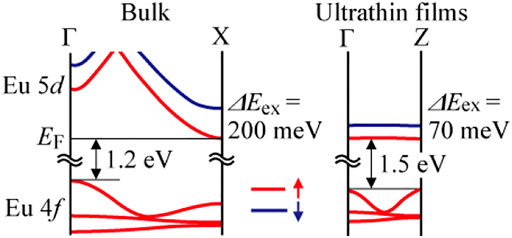
FIGURE 5. Band structure of the energy bands of the Eu 4f and Eu 5d states in EuO bulk and ultrathin films at the Γ and X points in the ferromagnetic phase. Solid and dashed lines correspond to majority and minority spin states, respectively.
Conclusion
In conclusion, we measured the temperature- and thickness-dependent 3D-ARPES spectra of single-crystalline EuO ultrathin films. The electronic structure of EuO ultrathin films changed from indirect to direct band gap at the X point. Both TC and ΔEEX gradually decreased with decreasing thickness. The decrease in neighboring atoms caused a suppressed hybridization between the Eu 4f and O 2p states and between the Eu 4f and 5d states, explaining the changes in the electronic structure and magnetic properties of EuO ultrathin films. The thickness dependences of the top of the Eu 4f state at the Γ and X points differ from each other because of the balance of the hybridization intensities between the Eu 4f–O 2p states and between the Eu 4f–Eu 5d states. A direct observation of the thickness-dependent variations in the electronic structure related to indirect- and super-exchange interactions is expected to provide a deeper understanding of low-dimensional magnetic ultrathin films. In the future, new applications such as photoluminescence using the direct band gap in EuO ultrathin films are expected.
Data Availability Statement
The raw data supporting the conclusions of this article will be made available by the authors, without undue reservation.
Author Contributions
HM and TH performed the experiments with assistance from MM, TI, and SK. MI performed the theoretical band structure calculations. HM and SK were responsible for the data analysis and writing of the paper. All the authors discussed the results and commented on the manuscript.
Funding
Part of this work was performed under the Use-of-UVSOR Facility Program (BL5U, 2012, 2013) of the IMS. This work was partly supported by the Grant-in-Aid for Scientific Research B (No. 22340107) and Grant-in-Aid for Challenging Exploratory Research (No. 10548960) from the Ministry of Education, Culture, Sports, Science and Technology of Japan. This project was supported by foundation of public interest of Tatematsu and Hibi science foundation.
Conflict of Interest
The authors declare that the research was conducted in the absence of any commercial or financial relationships that could be construed as a potential conflict of interest.
Publisher’s Note
All claims expressed in this article are solely those of the authors and do not necessarily represent those of their affiliated organizations, or those of the publisher, the editors, and the reviewers. Any product that may be evaluated in this article, or claim that may be made by its manufacturer, is not guaranteed or endorsed by the publisher.
References
Blaha, P., Schwarz, K., Sorantin, P., and Trickey, S. B. (1990). Full-potential, Linearized Augmented Plane Wave Programs for Crystalline Systems. Comput. Phys. Commun. 59, 399–415. doi:10.1016/0010-4655(90)90187-6
Dietrich, O. W., Henderson, A. J., and Meyer, H. (1975). Spin-wave Analysis of Specific Heat and Magnetization in EuO and EuS. Phys. Rev. B 12, 2844–2855. doi:10.1103/physrevb.12.2844
Eastman, D. E., Holtzberg, F., and Methfessel, S. (1969). Photoemission Studies of the Electronic Structure of EuO, EuS, EuSe, and GdS. Phys. Rev. Lett. 23, 226–229. doi:10.1103/physrevlett.23.226
Ghosh, D. B., De, M., and De, S. K. (2004). Electronic Structure and Magneto-Optical Properties of Magnetic Semiconductors: Europium Monochalcogenides. Phys. Rev. B 70, 115211. doi:10.1103/physrevb.70.115211
Ito, T., Kimura, S., Im, H., Nakamura, E., Sakai, M., Horigome, T., et al. (2007). AIP Conf. Proc. 879, 587.
Jensen, P. J., Dreyssé, H., and Bennemann, K. H. (1992). Calculation of the Film-Thickness-Dependence of the Curie Temperature in Thin Transition Metal Films. Europhys. Lett. 18, 463–468. doi:10.1209/0295-5075/18/5/015
Kasuya, T. (1970). Exchange Mechanisms in Europium Chalcogenides. IBM J. Res. Dev. 14, 214–223. doi:10.1147/rd.143.0214
Kasuya, T., and Yanase, A. (1968). Anomalous Transport Phenomena in Eu-Chalcogenide Alloys. Rev. Mod. Phys. 40, 684–696. doi:10.1103/revmodphys.40.684
Khomskii, D. I., and Sawatzky, G. A. (1997). Interplay between Spin, Charge and Orbital Degrees of Freedom in Magnetic Oxides. Solid State Commun. 102, 87–99. doi:10.1016/s0038-1098(96)00717-x
Larson, P., and Lambrecht, W. R. L. (2006). Electronic Structure and Magnetism of Europium Chalcogenides in Comparison with Gadolinium Nitride. J. Phys. Condens. Matter 18, 11333–11345. doi:10.1088/0953-8984/18/49/024
Lee, H., KimRho, J.-Y. K.-J., Rho, K.-J., Park, B.-G., and Park, J.-H. (2007). Temperature Dependent Phase Transition of EuO on MgO(100). J. Appl. Phys. 102, 053903. doi:10.1063/1.2775297
Mauger, A., and Godart, C. (1986). The Magnetic, Optical, and Transport Properties of Representatives of a Class of Magnetic Semiconductors: The Europium Chalcogenides. Phys. Rep. 141, 51–176. doi:10.1016/0370-1573(86)90139-0
Miyazaki, H., Im, H. J., Terashima, K., Yagi, S., Kato, M., Soda, K., et al. (2010). La-doped EuO: A Rare Earth Ferromagnetic Semiconductor with the Highest Curie Temperature. Appl. Phys. Lett. 96, 232503. doi:10.1063/1.3416911
Miyazaki, H., Ito, T., Im, H. J., Yagi, S., Kato, M., Soda, K., et al. (2013). J. Electron Spectrosc. Relat. Phenom. 191, 7.
Miyazaki, H., Ito, T., Im, H. J., Yagi, S., Kato, M., Soda, K., et al. (2009). Direct Observation of Momentum-dependent Exchange Interaction in a Heisenberg Ferromagnet. Phys. Rev. Lett. 102, 227203. doi:10.1103/physrevlett.102.227203
Miyazaki, H., Momiyama, H., Hajiri, T., Ito, T., Imura, K., Matsunami, M., et al. (2012). Fabrication of Single Crystalline EuO Thin Film with SrO Buffer Layer on SrTiO3substrate. J. Phys. Conf. Ser. 391, 012047. doi:10.1088/1742-6596/391/1/012047
Monteiro, P. M. S., Baker, P. J., Hine, N. D. M., Steinke, N-J., Ionescu, A., Cooper, J. F. K., et al. (2015). Elevated Curie Temperature and Half-Metallicity in the Ferromagnetic Semiconductor La X Eu 1 − X O. Phys. Rev. B 92, 045202. doi:10.1103/physrevb.92.045202
Negusse, E., Dvorak, J., Holroyd, J. S., Liberati, M., Santos, T. S., Moodera, J. S., et al. (2009). Magnetic Characterization of Ultrathin EuO Films with XMCD. J. Appl. Phys. 105, 07C930. doi:10.1063/1.3076044
Passell, L., Dietrich, O. W., and Als-Nielsen, J. (1976). Neutron Scattering from the Heisenberg Ferromagnets EuO and EuS. I. The Exchange Interactions. Phys. Rev. B 14, 4897–4907. doi:10.1103/physrevb.14.4897
Santos, T. S., and Moodera, J. S. (2004). Observation of Spin Filtering with a ferromagneticEuOtunnel Barrier. Phys. Rev. B 69 (R), 241203. doi:10.1103/physrevb.69.241203
Schiller, R., Müller, W., and Nolting, W. (2001). Kondo Lattice Model: Application to the Temperature-dependent Electronic Structure of EuO(100) Films. Phys. Rev. B 64, 134409. doi:10.1103/physrevb.64.134409
Schmehl, A., Vaithyanathan, V., Herrnberger, A., Thiel, S., Richter, C., Liberati, M., et al. (2007). Epitaxial Integration of the Highly Spin-Polarized Ferromagnetic Semiconductor EuO with Silicon and GaN. Nat. Mater 6, 882–887. doi:10.1038/nmat2012
Steeneken, P. G., Tjeng, L. H., Elfimov, I., Sawatzky, G. A., Ghiringhelli, G., Brookes, N. B., et al. (2002). Exchange Splitting and Charge Carrier Spin Polarization in EuO. Phys. Rev. Lett. 88, 047201. doi:10.1103/physrevlett.88.047201
Keywords: spintronic device, EuO, ultrathin films, photoemission spectroscopy, electronic structure
Citation: Miyazaki H, Hajiri T, Matsunami M, Inukai M, Ito T and Kimura S-i (2022) Observation of Thickness-Dependent Exchange Interaction in EuO Ultrathin Films. Front. Nanotechnol. 4:872717. doi: 10.3389/fnano.2022.872717
Received: 09 February 2022; Accepted: 13 May 2022;
Published: 30 June 2022.
Edited by:
Karthik Ramasamy, UbiQD, Inc., United StatesReviewed by:
Asish K. Kundu, Brookhaven National Laboratory (DOE), United StatesYukiaki Ishida, The University of Tokyo, Japan
Sanjoy Kr Mahatha, Thapar Institute of Engineering and Technology, India
Copyright © 2022 Miyazaki, Hajiri, Matsunami, Inukai, Ito and Kimura. This is an open-access article distributed under the terms of the Creative Commons Attribution License (CC BY). The use, distribution or reproduction in other forums is permitted, provided the original author(s) and the copyright owner(s) are credited and that the original publication in this journal is cited, in accordance with accepted academic practice. No use, distribution or reproduction is permitted which does not comply with these terms.
*Correspondence: Hidetoshi Miyazaki, bWl5YXpha2lAbml0ZWNoLmFjLmpw; Shin-ichi Kimura, a2ltdXJhLnNoaW4taWNoaS5mYnNAb3Nha2EtdS5hYy5qcA==
†Present address: Masaharu Matsunami, Toyota technological Institute, Nagoya, Japan
 Hidetoshi Miyazaki
 Tetsuya Hajiri2
 Shin-ichi Kimura