 Xiao-Hua Hu
 Shisheng Xiong*
- School of Information Science and Technology, Fudan University, Shanghai, China
Block copolymer (BCP) self-assembly, as a novel bottom-up patterning technique, has received increasing attention in the manufacture of nanodevices because of its significant advantages of high resolution, high throughput, low cost, and simple processing. BCP self-assembly provides a very powerful approach to constructing diverse nanoscale templates and patterns that meet large-scale manufacturing practices. For the past 20 years, the self-assembly of BCPs has been extensively employed to produce a range of nanodevices, such as nonvolatile memory, bit-patterned media (BPM), fin field-effect transistors (FinFETs), photonic nanodevices, solar cells, biological and chemical sensors, and ultrafiltration membranes, providing a variety of configurations for high-density integration and cost-efficient manufacturing. In this review, we summarize the recent progress in the fabrication of nanodevices using the templates of BCP self-assembly, and present current challenges and future opportunities.
Introduction
A seed of the nanotechnology concept was first planted by the famous physicist Feynman (1959) in his lecture There’s Plenty of Room at the Bottom. Later, the term “nano-technology” was coined by Taniguchi (1974) to describe the precision manufacture of materials with control of their dimensions on the order of a nanometer, and Drexler (1986) employed a related term “nanotechnology” in his book Engines of Creation: The Coming Era of Nanotechnology for depicting molecular nanotechnology. Over the past 60 years, nanotechnology has progressed tremendously and has been widely used in chemistry (Whitesides, 2005), biology (Sarikaya et al., 2003; Kim and Franco, 2020), physics (Omidian et al., 2021), materials science (Hu et al., 2016; Sun et al., 2020), and medicine (Silva, 2004; Sindhwani and Chan, 2021). Undoubtedly, nanofabrication technology plays the most important role in the development of nanotechnology because it can not only achieve the realization of sophisticated nanodevice concepts but also continuously improve the performance of nanodevices (Chen et al., 2021). Currently, there are two strategies for nanofabrication that are broadly employed in the manufacture of nanodevices: top-down and bottom-up (Chung et al., 2005; Hobbs et al., 2012; Mullen and Morris, 2021).
The top-down method involves physical processes such as cutting, slicing, or milling to break bulk material into desired nanoparticles or materials with controlled shapes and sizes (Mullen and Morris, 2021). For nanodevice fabrication, the top-down approach mainly employs lithography technologies that include deep ultraviolet (DUV) lithography (Sanders, 2010), extreme ultraviolet (EUV) lithography (Päivänranta et al., 2011), nanoimprint lithography (NIL) (Barcelo and Li, 2016), and electron beam lithography (EBL) (Chen, 2015). Among these technologies, DUV lithography is the most commonly used patterning technology in the semiconductor industry for manufacturing nanodevices.
The general concept of optical lithography uses light to transfer patterns from a photomask to photoresist films. The process includes spin-coating photoresist on a wafer, placement of a photomask on top, and changing the solubility of photoresist in the regions exposed to light irradiation (Mullen and Morris, 2021). For positive-tone photoresists, developing the photoresist selectively dissolves these regions of altered solubility, leaving a patterned photoresist on the wafer. The resultant photoresist pattern is used as a mask during subsequent pattern transfer steps to define features on the wafer. Currently, the theoretical and practical limits of the minimum pitch for 193 nm lithography is ∼80 nm with a single exposure (Pan, 2018). Although 193 nm lithography combined with the multiple patterning technology can further reduce the feature size, such steps increase the manufacturing cost and introduce unwanted process variation. As the most advanced lithography, EUV lithography at 13.5 nm is an extension of optical lithography and has achieved high-volume manufacturing at the 5-nm technology node. However, EUV lithography has its own challenges, such as extremely high tool cost and footprint requirements (Levinson and Brunner, 2018; Fourkas et al., 2021). NIL is a method for creating nanoscale patterns by mechanical deformation of a photoresist layer before cross-linking (Torres et al., 2003). It displays many advantages including simple processing, high throughput, and high resolution, but it still needs to face key challenges, such as high-fidelity duplication of the features at large areas and low-cost fabrication of large-area molds with a long lifetime (Chen et al., 2021). EBL can produce sub-10-nm resolution patterns without a mask. However, it possesses the fatal drawback of low throughput (Chen and Xiong, 2020). Comparatively, the bottom-up approach may provide a complementary nanofabrication route to the top-down methods that circumvent their challenges and disadvantages.
The bottom-up approach refers to the assembly of atoms or molecules into ordered nanostructure arrays (Mullen and Morris, 2021). Among them, block copolymer (BCP) self-assembly is one of the most popular bottom-up techniques for manufacturing nanodevices with feature sizes ranging from 5 to 100 nm because it has high throughput, high efficiency, excellent scalability, low cost, and compatibility with industrial semiconductor processes (Cummins and Morris, 2018; Hu and Xiong, 2021). The technique depends on BCP microphase separation to self-assemble into high-density and highly ordered pattern arrays with nanoscale features. The driving force of BCP self-assembly originates from the thermodynamic incompatibility between two blocks of the copolymer. Mansky et al. (1995) first reported the BCP self-assembly as a soft template for pattern transfer, where polystyrene-block-polybutadiene (PS-b-PB) microphase separation produced a spherical nanodomain structure after thermal annealing, and then hexagonal dot arrays were obtained by an etching process. Subsequently, they also fabricated perpendicularly oriented lamellae arrays by modifying the wettability of the substrate surface (Mansky et al., 1997). These two innovative works paved the way for the applications of BCP self-assembly in the fabrication of nanodevices. During the past 20 years, BCP self-assembly achieved great progress and created immense interest in semiconductor fabrication. To date, templates for BCP self-assembly were mainly used in the manufacture of nonvolatile memory devices (Guarini et al., 2003; Yoo et al., 2015), bit-patterned media (BPM) (Xiao et al., 2009; Griffiths et al., 2013), fin field-effect transistors (FinFETs) (Black, 2005; Liu et al., 2018), photonic nanodevices (Stefik et al., 2015; Alvarez-Fernandez et al., 2021), solar cells (Topham et al., 2011; Sadegh et al., 2021), chemical and biological sensors (Jeong et al., 2014; Kang et al., 2020), and ultrafiltration membranes (Jackson and Hillmyer, 2010; Guo et al., 2021), as shown in Figure 1.
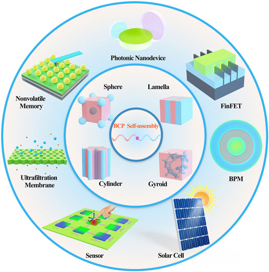
FIGURE 1. Templates made from BCP self-assembly offer various opportunities for nanodevice manufacturing.
In this article, we review the progress of BCP self-assembly in the formation of versatile templates for manufacturing nanodevices. We hope that this article can help researchers have a more comprehensive and in-depth understanding of BCP self-assembly in nanofabrication. Furthermore, we believe that this article will offer inspiration for scientists who want to further expand the practical applications of BCP templates.
Block Copolymer Self-Assembly
BCP is a type of copolymer with two or more chemically distinct homopolymer blocks that are connected by a covalent bond. The simplest BCPs are linear A-b-B diblock copolymers, in which block A and block B denote two different homopolymers that are joined together via a covalent bond. As we know, phase separation is a very common phenomenon in nature, such as the separation between oil and water, which originates from the incompatibility of the two phases. However, BCP phase separation occurs only on a microscopic scale due to the covalent bond between the two blocks. Microphase separation is a unique phenomenon of BCPs and endows BCPs with many significant characteristics compared to the corresponding random copolymers or homopolymer mixtures. BCPs self-assemble through microphase separation to form diverse morphologies that are determined by three key parameters (Bates and Fredrickson, 1990): the degree of polymerization (N), the volume fraction of block A (fA), and the Flory–Huggins interaction parameter of two blocks (χ). N and fA are determined through polymer synthesis, while χ is determined by the choice of the monomer pair. Based on the self-consistent field theory (SCFT), a theoretical phase diagram of A-b-B diblock copolymer can be created, as shown in Figure 2. The microphase separation strength of the BCP is directly related to χN. Figure 2 displays that the minimum segregation force (χN) for microphase formation is 10.5. When χN ≥ 10.5 (Pinto-Gómez et al., 2020), as fA changes, BCP microphase separates and self-assembles into ordered equilibrium structures with different morphologies, such as spheres (SPH), cylinders (CYL), gyroids (GYR), and lamellae (LAM). For the identical χN value, the equilibrium phases at fA and 1-fA share the same structure, but with an inverted arrangement. The equilibrium pitch size (L0) of a BCP can be determined based on the equation obtained from SCFT: L0 ≈ aχ1/6N2/3, where a is the statistical segment length (Bates and Fredrickson, 1990). Therefore, to obtain very small microphase segregated domains (e.g., L0 < 10 nm), it is necessary to develop a BCP with a high χ value but low N. In addition, the width of the interface between the two blocks can be estimated by aχ−1/2, which means for a BCP with a higher χ value, the interface between blocks is sharper, so the edge roughness is smaller (Bates and Fredrickson, 1990).
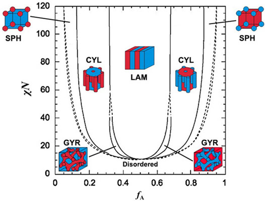
FIGURE 2. Theoretical phase diagram of diblock copolymer melts calculated by using the SCFT. The figure is reprinted with permission from Xu et al. (2020), copyright 2020, AIP Publishing.
In general, based on BCP self-assembly, four strategies are used to fabricate nanodevices. First, BCP templating is the most widely employed method for manufacturing nanodevices (Alvarez-Fernandez et al., 2021), as shown in Figure 3A. A BCP solution is spin-coated on a substrate to form a thin film. Its thickness can be precisely controlled by spin speed, volatility of the solvent, and concentration of the BCP solution. A thermal or solvent vapor annealing step is adopted to drive the BCP film to microphase separate. The structures from self-assembly (or directed self-assembly) of the BCP film are selectively etched to remove one of the blocks, and the remaining block acts as a soft template for further patterning. Second, sequential infiltration synthesis (SIS), based on atomic layer deposition (ALD), is a novel type of the BCP patterning technique (Figure 3B). After annealing, by using the SIS technique, metal oxides can be selectively deposited in the polar block of a BCP and govern the growth at a molecular level. For example, using the SIS technique can convert a thin film formed by BCP self-assembly to a nanoporous AlOx membrane that act as an ultrafiltration device (Zhou et al., 2017). Third, BCP co-assembly incorporates inorganic nanoparticles into the polar block of BCPs in bulk solution before deposition, and then inorganic nanoparticles will yield ordered nanostructures with BCP microphase separation (Figure 3C). The technique is broadly employed in the manufacture of photonic nanodevices (Guldin et al., 2013). Fourth, microphase-separated BCPs can be directly utilized to form functional structures of nanodevices, such as the preparation of nonvolatile memory by polyisoprene-block-maltoheptaose (PI-b-MH) (Hung et al., 2017) and photovoltaic cells by conjugated BCPs (Guo et al., 2013). The following sections will describe in detail these techniques of manufacturing nanodevices based on BCP self-assembly and directed self-assembly.
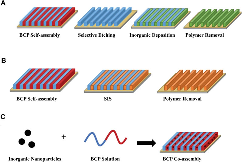
FIGURE 3. Schematics of the different strategies for designing nanodevice architectures by using BCP self-assembled films. (A) BCP templating. (B) BCP SIS. (C) BCP co-assembly. The figure is reprinted with permission from Alvarez-Fernandez et al. (2021), copyright 2021, Wiley-VCH.
Nonvolatile Memory
Nonvolatile memory is one of the most important components of an integrated circuit (IC). In recent years, it has continually developed in the direction of low power consumption, small size, long lifetime, and robust endurance. BCP self-assembly can prepare large-scale and high-density nanostructure arrays at a low cost, which has attracted considerable interest in the field of nonvolatile memory manufacturing. BCP self-assembly yields uniform nanostructures that can be used not only as a mask for pattern transfer but also directly as a functional layer of memory devices. As a mask, Guarini et al. (2003) have proposed an approach based on BCP self-assembly to fabricate silicon nanocrystal flash memory. Cylinder-forming polystyrene-block-poly(methyl methacrylate) (PS-b-PMMA) is spin-coated on a substrate to form a thin film and then annealed to generate hexagonally close-packed PMMA cylinders in a PS matrix. The PMMA domains are completely removed, leaving a porous PS film with a diameter of ∼20 nm and a center-to-center spacing of ∼40 nm as a mask to define silicon nanocrystals. The flash memory devices are completed by depositing silicon oxide on the top of the silicon nanocrystal array, and then depositing, doping, and patterning the polysilicon gate. Finally, a fabricated flash memory device displays a low operating voltage, excellent retention time (>106 s), and good endurance (>109 cycles). Subsequently, a metal nanodot memory has been prepared using a self-assembled BCP lift-off technique whose detailed process flow is described in Figure 4A (Hong et al., 2010). A Cr nanodot memory with a density of 1.2 × 10¹¹ devices/cm2 displays a 15 V ultrawide memory window that has been fabricated (Figure 4B), which is very suitable for multilevel cell operations. It also possesses a low leakage current density (<5 × 10⁻⁷ A/cm2 at ± 18 V) (Figure 4C). In addition, using a self-assembled BCP lift-off process has successfully constructed bilayer Pt–Ti top electrodes arranged in periodic arrays with a diameter of 28 nm and a density of 5 × 10¹⁰ devices/cm2 (Frascaroli et al., 2015). These metal nanodot memory devices formed from simple and cost-effective BCP templating may create new opportunities for terabit memory applications.
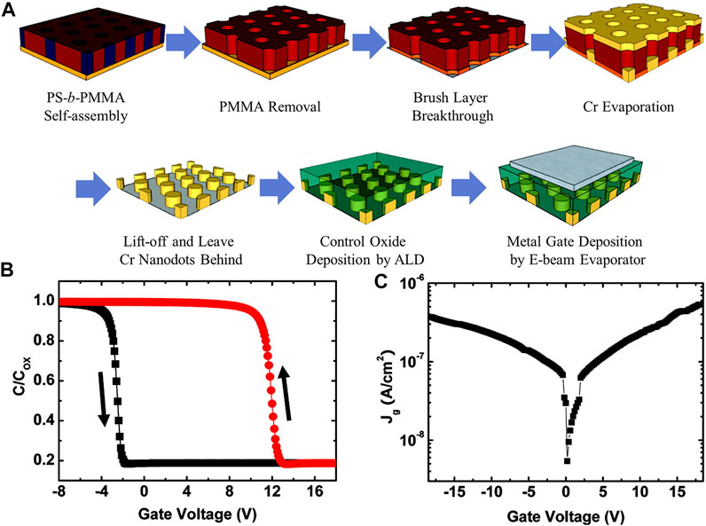
FIGURE 4. (A) Schematic process flow of the proposed metal nanodot memory fabrication using a self-assembled BCP lift-off. (B) Capacitance–voltage curve of the prepared nanodevice showing memory function. (C) A memory nanodevice showing low leakage current density. The figure is reprinted with permission from Hong et al. (2010), copyright 2010, American Chemical Society.
As a functional layer, SiOx has excellent insulating properties and is widely employed in constructing nonvolatile memory. Among BCPs, polystyrene-block-polydimethylsiloxane (PS-b-PDMS), as a common silicon-containing material, can form large-scale and uniform-sized SiOx nanostructures by self-assembly, and has gained broad attention. As shown in Figure 5A, ultrahigh-density and highly ordered SiOx nanodot memristors were directly formed on graphene electrodes via the self-assembly of PS-b-PDMS and subsequent etching without depending on expensive lithography tools and complex pattern transfer techniques (Park et al., 2012). The fabricated memristors exhibited unipolar switching features with reasonable set and reset voltages for resistive memory applications. For phase-change memory (PCM), the power consumption of a nanodevice can be dramatically reduced by inserting a PS-b-PDMS self-assembled SiOx nanostructure between a heating electrode and a phase-changing material (Figure 5B). As the fill factor of the SiOx nanostructure increases from 9.1 to 63.6%, the switching power of the PCM devices is reduced 20-fold (Park et al., 2013). The self-assembled SiOx nanostructures reduce the contact area between the heating electrode and the phase change material, thereby modifying the temperature profiles and reducing the threshold switching voltage and reset current. For unipolar NiO-resistive memory devices (Figure 5C), adding BCP self-assembled SiOx nanodots between the Pt and Ni electrodes can alter both the electric field and temperature distribution, thereby significantly reducing the variations of set and reset voltages as well as the standard deviation of the high resistance state (You et al., 2014). In addition, the SiOx nanodots can govern the resistive switching operation by selective NiO filament growth or rupture. Furthermore, BCP templates can also be used in flexible memory devices to improve their electrical performance. In Figure 5D, SiOx nanostructures made from PS-b-PDMS were incorporated with a flexible PCM device as nano-insulators to reduce the operating current by a factor of four. These uniformly aligned SiOx nanostructures can also reduce thermal stress in the PCM device and ultimately achieve reliable operation over more than 100 switching cycles and 1,000 bending cycles (Mun et al., 2015).
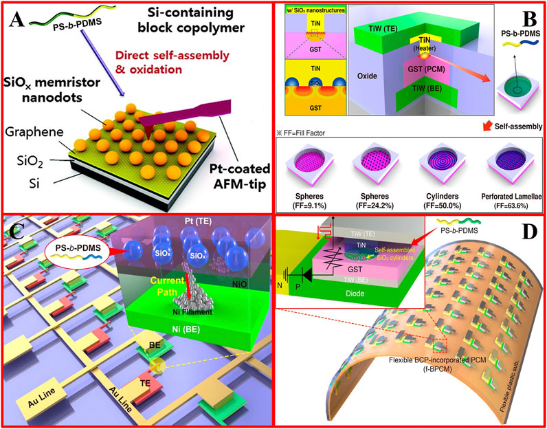
FIGURE 5. (A) Schematic diagram of sphere-forming BCPs that was used for preparing SiOx nanodot memristors. The figure is reprinted with permission from Park et al. (2012), copyright 2012, American Chemical Society. (B) Schematic diagram of a PCM device with different morphologies of SiOx nanostructures. The figure is reprinted with permission from Park et al. (2013), copyright 2013, American Chemical Society. (C) Schematic diagram of NiO memory with SiOx nanodots. The figure is reprinted with permission from You et al. (2014), copyright 2014, American Chemical Society. (D) Schematic diagram of flexible BCP-incorporated PCM arrays with diodes on a plastic substrate. The figure is reprinted with permission from Mun et al. (2015), copyright 2015, American Chemical Society.
Additionally, several novel architectural nonvolatile memory nanodevices have been developed with BCP templates. For example, some new methods have been proposed to construct nonvolatile organic field-effect transistor (OFET) memory with excellent performance, which include inserting Au nanoparticles (Leong et al., 2008), Pt nanoparticles (Chen et al., 2012), fullerene derivatives (Chen et al., 2012), and graphene (Khawas et al., 2018) in the P4VP domains of a polystyrene-block-poly(4-vinylpyridine) (PS-b-P4VP) template and embedding functionalized TiO2 nanoparticles in the PS block of a polystyrene-block-poly(ethylene oxide) (PS-b-PEO) template (Kirschner et al., 2017). These dopants enter one of the blocks with BCP microphase separation and become the charge storage components of nonvolatile OFET memory. Additionally, the self-assembly of PI-b-MH has yielded vertical cylinder, horizontal cylinder, and order-packed sphere of MH domains in a PI matrix (Hung et al., 2017). The PI and MH domains act as stretchable matrices and charge-trapping sites, respectively. Nonvolatile write-once-read-many-times memory, flash memory, and volatile dynamic random-access memory can be fabricated by controlling the orientations and morphologies of MH domains. Similarly, memory nanodevices have also been successfully obtained by using poly(n-butyl acrylate)-block-maltoheptaose (PBA-b-MH) with linear AB-type, ABA-type, and star-shaped architectures (Hung et al., 2018); polystyrene-block-maltoheptaose (PS-b-MH) with different morphologies and orientations (Chuang et al., 2020); or poly(9,9-di-n-hexyl-2,7-fluorene)-block-poly(δ-decanolactone) (PF-b-PDL) with AB, AB2, and AB3 architectures (Hsu et al., 2021). Moreover, an ultrafast photo-responsive nonvolatile flash memory was prepared by combining a BCP template with perovskite (Chang et al., 2020). Interestingly, a photonic transistor memory with photo-writing and electrical-erasing features has also been fabricated based on a polystyrene-block-poly(9,9-dioctylfluorene) (PS-b-PFO) template as a floating gate, where a high PS content is helpful for improving the memory performance (Chen et al., 2021).
In short, BCP self-assembly is very suitable for creating a wide variety of high-performance and high scalability memory nanodevices in a cost-effective manner.
Bit Patterned Media
A conventional hard disk drive (HDD) depends on magnetic grains for data storage. Unfortunately, storing a data “bit” requires an ensemble of irregular grains, which severely restricts the improvement of HDD storage density. BPM has been proposed as a novel data storage technology to greatly increase the areal density of HDD, effectively reduce the magnetic interference between neighboring bits, and dramatically improve the thermal stability (Griffiths et al., 2013). It consists of a highly ordered array of isolated magnetic islands, in which each magnetic island stores one bit, instead of recording a bit on an ensemble of grains. BCP self-assembly is a very promising candidate to manufacture BPM, which has many merits such as high resolution, high throughput, and low cost. Early work has focused on employing BCP self-assembled templates to directly pattern the magnetic thin film. For instance, Cheng et al. (2001) have fabricated single-domain Co nanodot arrays on a large area by using templates of self-assembled polystyrene-block-polyferrocenyldimethylsilane (PS-b-PFDS). In another work, faceted surfaces of commercially available sapphire wafers have been used for inducing the self-assembly of cylinder-forming PS-b-PEO over an arbitrarily large area (Park et al., 2009). As the molecular weight of PS-b-PEO decreases from 26.5 to 7.0 kg/mol, the areal density of the self-assembled PEO cylindrical domains increases from 0.74 to 10.5 Tb/in2. These BCP templates are very promising candidates to fabricate ultrahigh-density magnetic recording media. More recently, sub-20 nm Co–Pt dots with uniaxial perpendicular anisotropy (Sun et al., 2012) and Co–Pd multilayered nanopillar arrays (Owen et al., 2017) have been obtained with templates made from self-assembled PS-b-PFDS. However, it is impossible to construct uniform patterns over a large area with circular symmetry by using BCP self-assembly alone. Combing BCP self-assembly with EBL or NIL, uniform circular symmetry patterns can be generated (Ji et al., 2016). Sphere-, cylinder-, and lamella-forming BCPs have all been used to fabricate BPM nanodevices. For example, Xiao et al. (2005) employed BCP templates to yield uniform magnetic metal dots that can be applied to magnetic recording media. Yang et al. (2009) have reported using EBL to produce sparse chemical patterns which guide BCP self-assembly to construct high-density nanostructure arrays. Focusing on BPM applications, the directed self-assembly of cylinder-forming PS-b-PMMA implemented on a chemically pre-patterned substrate has been used to fabricate over an arbitrarily large area of vertical and cylindrical pore nanostructures with a density of 1 Tb/in2 (Yang et al., 2009). In addition, the use of sphere-forming PS-b-PDMS (Yamamoto et al., 2012; Xiao et al., 2014) and cylinder-forming PS-b-PMMA (Yang et al., 2014) has also been reported to manufacture integrated templates with both data and servo fields. In these cases, the pre-pattern guides of the BCP self-assembly were prepared by NIL.
However, BPM with a high densely packed nanodot array may bring some challenges for nanodevice fabrication because the read–write head needs to be smaller than the track width to guarantee accurate writing and reading of data. To circumvent the limit, an innovative BPM architecture has been proposed, which uses rectangular bits to store data. A greater bit aspect ratio is the main advantage of rectangular data bits, which is helpful for integrating BPM into a HDD. To date, there are two strategies to obtain rectangular bit patterns. The first approach is to combine EBL and BCP self-assembly (Ruiz et al., 2011). The detailed process flow is shown in Figure 6A. The EBL-prepared sparse stripe pattern directs the self-assembly of lamella-forming PS-b-PMMA to produce high-density and long-range ordered line arrays. After PMMA removal, a new layer of electron-beam resist is coated on the remaining PS stripes, and an orthogonal stripe pattern is written by EBL. Finally, highly uniform PS rectangular bit arrays with a critical dimension of 16 nm and a full pitch of 27 nm are successfully obtained by O2 plasma etching (Figure 6B). These high-density rectangular bit patterns are very suitable for manufacturing BPM with a high bit aspect ratio.
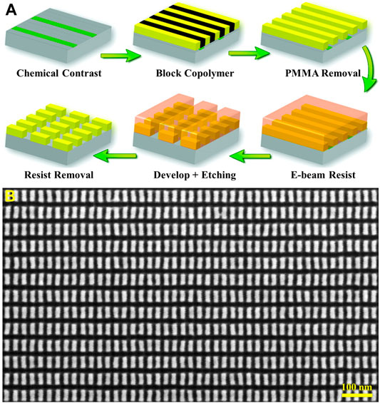
FIGURE 6. (A) Schematic diagram of fabricating rectangular patterns with arbitrary aspect ratio from lamellar phase BCP stripes. (B) SEM micrographs of PS rectangular patterns at the end of the process. The full pitch in the horizontal and vertical directions is 27 and 54 nm, respectively. The figure is reprinted with permission from Ruiz et al. (2011), copyright 2011, American Chemical Society.
The second method, developed by Wan et al. (2012), involves EBL, BCP self-assembly, and a double imprint process. Figure 7A displays the process flow. First, a rotary EBL is applied to separately create circumferential and radial striped chemical patterns that guide BCP-directed self-assembly. Then, highly uniform line arrays are obtained by directed self-assembly of lamella-forming PS-b-PMMA on chemical patterns on two separate sub-master templates, one with circumferential lines to define concentric tracks (Figure 7B) and a second with radial lines of constant angular pitch (Figure 7C). Finally, the master template of rectangular bits (Figure 7D) is fabricated by cross-cutting of circumferential and radial lines. Figure 7E shows an imprinted resist pattern from the final master template. The most attractive feature of the double imprint technique is that it can generate a master template by employing BCP self-assembly with flexibility, efficiency, and low cost, and construct numerous replicas for high-volume patterning on a media layer.
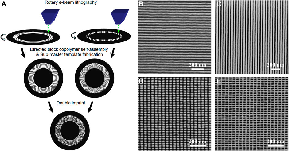
FIGURE 7. (A) Fabrication of nanoimprint templates with rectangular patterns using BCP lithography and double nanoimprint. SEM images of (B) the directed self-assembly of PS-b-PMMA lamellae with a full pitch of 27 nm on a sparse circumferential line chemical pattern after PMMA removal, (C) the directed self-assembly of PS-b-PMMA lamellae with a full pitch of 41 nm on sparse radial-line chemical patterns after PMMA removal, (D) the nanoimprint master template with rectangular patterns, and (E) the imprinted resist pattern from the master template. The figure is reprinted with permission from Wan et al. (2012), copyright 2012, SPIE.
The circumferential and radial line patterns are usually generated by using lamella-forming PS-b-PMMA. Unfortunately, the minimum full period accessible using lamella-forming PS-b-PMMA stops at 22 nm, which limits the preparation of a rectangular bit pattern with a density above 1.5 Tb/in2 (Ji et al., 2016). Subsequently, two approaches have been developed to overcome the dilemma of high-density BPM manufacturing. One approach is adding a self-aligned double patterning (SADP) step (Doerk et al., 2015), and the other is using high χ BCPs instead of PS-b-PMMA (Xiong et al., 2016). For the former, the chemical pattern of radial lines is first generated by rotary EBL. A lamella-forming PS-b-PMMA with a 22-nm full pitch self-assembles on the chemical pattern, and then pattern transfer is employed to generate the mandrel lines. Radial lines with an 11-nm full pitch are obtained by combining PS-b-PMMA self-assembly with SADP, which can be used to fabricate the rectangular bit patterns at a density above 1.5 Tb/in2 (Doerk et al., 2015). For the high χ BCP, Xiong et al. (2016) proposed to use lamella-forming poly(2-vinyl pyridine)-block-polystyrene-block-poly(2-vinyl pyridine) (P2VP-b-PS-b-P2VP) instead of PS-b-PMMA to acquire circumferential and radial lines with feature sizes below 10 nm. In the future, the density of rectangular bit patterns can be further increased by employing the smaller pitch of high χ BCPs, such as polytrimethylsilylstyrene-block-polylactide (Cushen et al., 2012), poly(3-hydroxystyrene)-block-polydimethylsiloxane (Azuma et al., 2018), polystyrene-block-polydihydroxystyrene (Kwak et al., 2017), polystyrene-block-poly(glycerol monomethacrylate) (Jeong et al., 2017), polystyrene-block-poly(hydroxyisobutylene) (Zhang et al., 2018), and polystyrene-block-poly(acrylic acid) (Yu et al., 2019).
In general, there are three primary reasons for BCP self-assembly to become one of the most promising techniques for high-volume manufacturing of BPM nanodevices. The first one is the high defect tolerance for magnetic recording media. The second one is that BCPs self-assemble with a high resolution, robust flexibility, and low cost. The third one is that BPM nanodevices are usually composed of simple periodic nanostructures with little or no overlay requirement during fabrication, particularly when compared with complex IC chip manufacturing.
Fin Field-Effect Transistors
FinFET as a new type of transistor architecture was invented in 1999 to satisfy the strong requirements of the semiconductor industry for device scaling and performance enhancement (Hu and Xiong, 2021). Compared with conventional complementary metal-oxide-semiconductor (CMOS) transistors, FinFETs are endowed with better performance, smaller size, and lower power consumption. FinFET devices are made up of multiple closely packed straight channels, which can be generated by using the directed self-assembly of cylinder- and lamella-forming BCPs at a high resolution and low cost.
The beautiful idea of integrating directed self-assembly of BCPs into FinFET fabrication was first proposed by Black (2005). In this case, the silicon fins with critical dimensions (width of 15 nm, height of 15 nm, and pitch of 40 nm) were obtained through the directed self-assembly of cylinder-forming PS-b-PMMA, and fabricated FinFET nanodevices had a current on–off ratio of ∼1 × 10⁵. Later, Tsai et al. (2014) prepared the first functional FinFET nanodevice with 29-nm pitch fins by employing the directed self-assembly of lamellar-forming PS-b-PMMA (Figure 8). The FinFET nanodevice displayed reasonable electrical performance, including a low drain-induced barrier lowering, a subthreshold slope of 70 mV/decade, and a current on–off ratio of 1 × 10⁵. Based on the directed self-assembly of lamella-forming PS-b-PMMA, the fabrication of FinFET nanodevices with a 27-nm pitch fin structure was also demonstrated on a 300-mm pilot line that integrated with 193-nm immersion lithography and standard semiconductor manufacturing processes (Liu et al., 2016). High aspect ratio silicon fin structures with 100 nm height and a critical dimension of 8–10 nm were constructed. In addition, the directed self-assembly of a high χ BCP was also adopted to fabricate FinFET nanodevices that displayed higher resolution (24 nm pitch), smaller line edge roughness, and smaller line width roughness than PS-b-PMMA (Tsai et al., 2016).
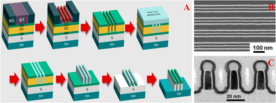
FIGURE 8. (A) Schematic diagram of the process flow of forming FinFET using a BCP self-assembled template. (B) SEM image of a group of fins. (C) TEM image of 29-nm pitch silicon on insulator fins. The figure is reprinted with permission from Tsai et al. (2014), copyright 2014, American Chemical Society.
Furthermore, Liu et al. (2018) demonstrated an electrical validation of the directed self-assembly of BCPs in the fabrication of 7-nm node FinFET devices by employing IBM’s full 7-nm ground-rule process in a 300-mm wafer high-volume-manufacturing compliant facility. The critical dimension of the generated fin structure was approximately 11.2 nm. Compared with self-aligned quadruple patterning (SAQP) achieved through IBM’s same 7-nm technology, the directed self-assembly of BCPs to form FinFETs displayed a better and narrower channel resistance distribution in short channel devices, and a slightly higher threshold voltage and a lower subthreshold swing (close to the theoretical limit of 60 mV/decade) in long channel devices, which suggested better pitch-walking control. Additionally, by employing BCP self-assembly to manufacture FinFET nanodevices, the total processing cost and the number of process steps can be reduced by ∼9.5 and 30%–40%, respectively. In a separate work, using templates made from the self-assembly of lamellar-forming PS-b-PMMA, InAs FinFET nanodevices with a 15-nm width fin have been prepared by Cerba et al. (2019). Electrical measurements demonstrate that the drain currents of the 100- and 200-nm long InAs fins are 70 and 2 μA, respectively. The ensemble of these different results implies that the directed self-assembly of BCPs could become a low-cost and simplified patterning technique for high-volume manufacturing of FinFET nanodevices in the semiconductor industry.
To summarize, the directed self-assembly of BCPs has become one of the most promising approaches for the fabrication of sub-10-nm FinFETs as an alternative to expensive multiple patterning technologies.
Photonic Nanodevices
To date, the interaction of light with matter is one of the hottest research topics in science and technology communities. The ability to control and modulate the interaction of light with matter is vital to obtaining desired optical properties such as reflection, refraction, transmission, and selective polarization (Stefik et al., 2015). Accurate control of the morphology and composition of optical materials can build periodic interactions with light on wavelength and sub-wavelength scales. Fortunately, the self-assembly of BCPs provides a simple, convenient, and low-cost strategy to construct photonic nanodevices with a variety of complex architectures. Currently, two specific routes have been broadly adopted: BCP co-assembly (Hoheisel et al., 2015; Sarkar and Alexandridis, 2015; Stefik et al., 2015) and BCP templating (Kim et al., 2016; Hulkkonen et al., 2018; Zhou et al., 2020).
For BCP co-assembly, inorganic nanoparticles are introduced into a single block of amphiphilic BCPs through intermolecular forces in bulk solution. For nanoparticles to conduct co-assembly into a BCP, it is necessary to balance the conformational entropy of the BCP, the insertion enthalpy of the nanoparticles into the BCP, and the translational entropy of the nanoparticles (Alvarez-Fernandez et al., 2021). For example, Guldin et al. (2013) have proposed to co-assemble TiO2 nanocrystals, a silica-based sol, and polyisoprene-block-poly(ethylene oxide) (PI-b-PEO) in a mixture solution of toluene and n-butanol. The inorganic components are selectively deposited in the PEO block. PI-b-PEO undergoes self-assembly to produce a cubic architecture with PI spheres on transparent substrates, and the inorganic components stay in the PEO matrix. The inorganic hybrid (silica-based sol and TiO2 nanocrystals) thin films with an inverse opal-type structure are fabricated by removing the polymer and serve as self-cleaning antireflective optical coatings with light transmittance of up to 99.9% at 540 nm. The main advantage of co-assembly is the precise control of the concentration and size of the guest nanoparticles in the final material. However, microphase separation of BCPs becomes very difficult at a large nanoparticle size or high nanoparticle loading, which restricts the applicability of BCP co-assembly.
BCP templating provides an alternative approach to avoid the aforementioned limitations. As shown in Figure 9A, hexagonal metal nanoparticle arrays have been generated from cylinder-forming PS-b-PMMA self-assembled templates and have been further ensembled by using pattern shrinkage, resulting in an increased refractive index of 5.1 (Kim et al., 2016). Furthermore, over 100-nm wavelength bandwidths, the effective refractive index can remain above 3 (Figure 9B).
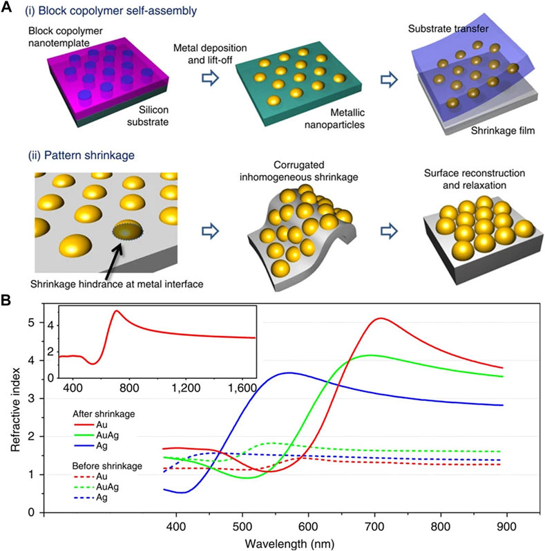
FIGURE 9. (A) Schematic for metal nanoparticle ensemble preparation by (i) BCP self-assembly and substrate transfer and (ii) pattern shrinkage. (B) Ellipsometry measurements of refractive indices of Au, Ag, and Au–Ag alloy nanoparticle ensembles before (dashed line) and after (solid line) pattern shrinkage. The figure is reprinted with permission from Kim et al. (2016), copyright 2016, Springer Nature.
Hulkkonen et al. (2017) explored the use of BCP self-assembly to adjust the optical properties of silicon. Cylinder-forming PS-b-P2VP templates were employed as an etch mask to fabricate pore silicon arrays on a macroscopic scale. The diameter and porosity of the silicon holes could be precisely governed through etching time. The volume-averaging theory and two-dimensional (2D) Maxwell−Garnett theory were used to characterize the optical features of the porous silicon, and the results demonstrated that the refractive index and reflectance at 500 nm of the porous silicon could be maximum reduced by 30 and 62%, respectively, compared to bulk silicon. In addition, large-area and highly ordered silicon nanopillar arrays with a high aspect ratio were fabricated through the self-assembly of PS-b-P2VP (Mokarian-Tabari et al., 2017). These silicon nanopillars could act as an antireflective functional layer, and the reflectivity decreased as the height of the nanopillar increased. When the height of the silicon nanopillars was ∼115 nm and the period was ∼200 nm, its reflectivity was less than 0.16%, reduced by 100 times over a wavelength range of 400–900 nm at a 30° incidence angle, compared with planar silicon. Moreover, the reflectivity stayed below 1.75% at a 75° incident angle.
Rasappa et al. (2018) reported on integrating the directed self-assembly of BCPs with soft NIL to prepare optical nanoresonators. Directed self-assembly of lamella-forming PS-b-PDMS on a guiding pattern that was prepared by NIL, followed by etching, obtained highly ordered and wafer-scale silicon nanofin arrays with a feature size of sub-10 nm and a height of ∼125 nm. The silicon nanofins were employed as a photonic-guided-mode resonance filter. The sensitivity of the nanodevice filters as a refractive index sensor could be enhanced by reducing the feature size of the nanofins.
Based on BCP self-assembly, all-metal broadband optical absorbers were prepared by Hulkkonen et al. (2018). The self-assembly of PS-b-P2VP yielded a hexagonal dot pattern that was transferred onto a silicon substrate through an etching process. Au was deposited on the silicon templates with high-density and highly ordered holes by an electron-beam evaporator, and then it was transferred onto a transparent plate to form uniform Au nano-dome arrays as an optical absorber. The results displayed that over 97% of visible light could be absorbed in direct incidence by 80-nm tall Au nano-dome arrays. Additionally, the all-metal broadband optical absorber was not sensitive to polarized light because of its structure symmetry. Employing BCP templates, well-ordered arrays of Au nanoparticles for optical applications were fabricated by Jin et al. (2018) and Alvarez-Fernandez et al. (2020).
Interestingly, the BCP self-assembly was used to construct complex three-dimensional (3D) architectures for optical applications (Stefik et al., 2015). For example, the self-assembly of polyisoprene-block-polystyrene-block-poly(ethylene oxide) (PI-b-PS-b-PEO) was carried out to form a gyroid nanostructure template (Vignolini et al., 2012). The template was employed for generating ordered 3D Au metamaterials that show optical chirality and orientation-dependent color under linearly polarized incident light. Separately, gyroid-forming PI-b-PS-b-PEO was used for fabricating 3D hollow Au struts (Salvatore et al., 2015). The optical transmission of the hollow Au struts was increased nearly threefold with respect to a full Au gyroid. The wall thickness of the 3D hollow Au struts had a great influence on the overall optical transmission.
In short, BCP self-assembly offers a simple, rapid, straightforward, and cost-effective approach for fabricating new functional photonic nanodevices with high scalability and reproducibility.
Solar Cells
A solar cell, also called a photovoltaic cell, is an electrical device that converts light energy directly into electricity via the photovoltaic effect. It has become one of the most promising candidates for the production of renewable and clean energy (Li et al., 2020). Recently, BCP self-assembly has received considerable attention for manufacturing solar cells due to its easy fabrication, high efficiency, low cost, low weight, and environmental friendliness (Topham et al., 2011). The role of BCPs in photovoltaic devices can be mainly divided into two types: directly as active materials and indirectly as structure directors (Darling, 2009).
As active materials, conjugated BCPs are widely adopted in solar cells due to their excellent conductivity and charge mobility. For example, poly(4-vinyltriphenylamine)-block-poly(perylene bisimide acrylate) (PvTPA-b-PPerAcr) has been utilized as an active layer and has displayed a much higher power conversion efficiency (PCE) than the same components in homopolymer-based photovoltaic devices (Lindner et al., 2006). Here, the hole transport is mediated through the PvTPA block, and both electron transport and light absorption take place in the PPerAcr block (Lindner and Thelakkat, 2004). The PvTPA-b-PPerAcr self-assembles into nanostructured bulk heterojunctions, offering nanoscale charge separating interfaces, which is beneficial to improve PCE. In another example, poly(3-butylthiophene)-block-poly(3-octylthiophene) (P3BT-b-P3OT) blended with fullerene derivative (PC71BM) has been used as the active materials of solar cells and achieved a 3.0% PCE (Ren et al., 2010). The blends had an interpenetrating morphology with 11–18-nm crystalline domains that can enhance the carrier mobility of holes in devices compared to devices made with the parent homopolymers. Similarly, a PCE of 4.02% has been achieved in a photovoltaic device made with poly(3-butylthiophene)-block-poly(3-hexylthiophene)/PC71BM (He et al., 2011). In recent years, many conjugated BCPs have been developed as active materials in solar cells, such as poly(3-hexylselenophene)-block-poly(3-hexylthiophene) (Gao et al., 2012), poly(3-hexylthiophene)-block-poly((9,9-dioctylfluorene)-2,7-diyl-alt-[4,7-bis(thiophen-5-yl)-2,1,3-benzothiadiazole]-2′,2″-diyl) (Guo et al., 2013), poly(2,5-dihexyloxy-p-phenylene)-block-poly(3-hexylthiophene) (Lee et al., 2015), and poly(3-hexylthiophene)-block-poly(dithienosilole-diketopyrrolopyrrole) (Idriss et al., 2020).
BCP templating, in which the BCP is utilized as a sacrificial etch mask, offers a platform to pattern active layers. For instance, Crossland et al. (2009) have reported that self-assembled BCP templates were employed to fabricate a solar cell with a PCE of 1.7%. As shown in Figure 10, poly(4-fluorostyrene)-block-polylactide (PFS-b-PLA) self-assembles into an ordered bicontinuous gyroid morphology. After the removal of the PLA block, a voided PFS gyroid template is obtained and used to yield a TiO2 gyroid network through electrochemical deposition. Then, the PFS template is completely removed, and a free-standing gyroid network array is formed. Finally, a bicontinuous bulk heterojunction solar cell is produced via backfilling with a solid-state hole transporting material and capping with a counter electrode. In another example, vertical nanorods and nanowalls of TiO2 have been fabricated by a BCP template strategy and then utilized as the electron transport layer of perovskite solar cells (Seo et al., 2016). A TiO2 nanorod-based perovskite solar cell has exhibited better reproducibility and performance than solar cells made with TiO2 nanowalls, and its PCE was determined to be 15.5%. TiO2 nanorods serve as scaffolds in the perovskite solar cells, resulting in the full coverage of perovskite capping layers and thereby achieving a more efficient charge separation and lower charge recombination. Similarly, mesoporous NiOx as a hole transport layer of perovskite solar cells can be also fabricated via the BCP template-assisted method (Sadegh et al., 2021). In these perovskite solar cells, the high-quality mesoporous NiOx structure can significantly inhibit charge recombination and promote charge transportation, leading to a high PCE of 20.2%. Interestingly, self-assembled poly(3-hexylthiophene)-block-polylactide (P3HT-b-PLA) can be used both as active materials and as templates to pattern active materials into organized nanostructures (Botiz and Darling, 2009). These works demonstrate that using BCP-patterned active materials play an important role in enhancing the performance of photovoltaic devices.
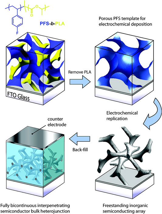
FIGURE 10. Schematic representation of gyroid network replication from BCP templates and the assembly of hybrid solar cells. The figure is reprinted with permission from Crossland et al. (2009), copyright 2009, American Chemical Society.
In summary, BCP self-assembly offers a powerful platform in terms of both techniques and materials for manufacturing higher efficient and more economic solar cells.
Sensors
Sensors are a type of device that possess the capability of detecting the composition and concentration of target substances. They play a significant role in contemporary life and are commonly applied in the environmental and biomedical fields. BCP self-assembly has gained great attention in the field of sensors because it can offer a simple and cost-effective strategy to fabricate highly ordered nanostructure arrays over a large area.
By using poly(ethylene oxide)-block-poly(propylene oxide)-block-poly(ethylene oxide) (PEO-b-PPO-b-PEO) templates, a mesoporous silica film was prepared and served as a gas sensor for detecting NO and NO2 gases (Yamada et al., 2003). The sensitivities of the sensor for NO and NO2 were determined to be 100 and 50 ppm, respectively. Afterward, a NO2 gas sensor with enhanced performance was fabricated based on a BCP template (Yun et al., 2018). As shown in Figure 11A, the self-assembly of PS-b-PMMA generated large-area and highly ordered nanostructures with vertical PS cylinders in a PMMA matrix. The nanostructures were etched to remove the PMMA matrix and leave the PS cylinders as a template to prepare a Mo nanomesh. The Mo nanomesh could be easily converted into a MoS2 nanomesh via sulfurization chemical vapor deposition. Figure 11B shows that the MoS2 nanomesh possessed a distinctive high sensitivity for NO2 at 1 ppm. Compared to a MoS2 thin film, the MoS2 nanomesh exhibited a 7-fold enhancement (Figure 11C) and superior reversibility for NO2 sensitivity at room temperature and 80% relative humidity (RH).
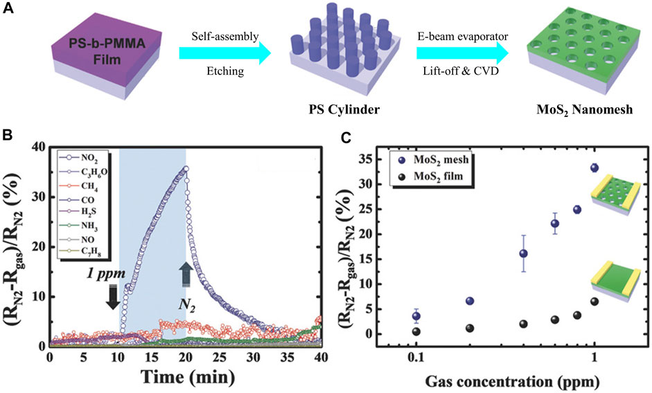
FIGURE 11. (A) Schematic illustration of the synthesis of MoS2 nanomesh by BCP self-assembly. (B) Selective property of the MoS2 nanomesh toward 1 ppm of various gas molecules at 80% RH. (C) NO2 sensing response over a concentration range of 0.1–1 ppm at room temperature and 80% RH. The figure is reprinted with permission from Yun et al. (2018), copyright 2018, Wiley-VCH.
Cylinder-forming PS-b-PDMS underwent self-assembly in a confined groove to generate an array of highly ordered 15-nm wide nanowires (Jung et al., 2008). The BCP template was directly used for patterning poly(3,4-ethylenedioxythiophene):poly(styrenesulfonate) (PEDOT:PSS) to fabricate conducting polymer nanowires that act as an ethanol gas sensor with high sensitivity. In a separate work (Guo et al., 2016), 3D ZnO gyroidal nanostructures exhibited a very sensitive capacity for distinguishing ethanol gas. The 3D ZnO nanostructures were generated by replicating BCP templates with a gyroid morphology via ALD. By tuning the ALD cycles, solid nanorod and hollow nanotube structures of ZnO were fabricated. Compared with the solid nanorods, the 3D ZnO gyroidal nanotubes displayed a higher sensitivity to ethanol gas. The gyroidal nanotubes of ZnO can also be employed as a sensor to detect formaldehyde at concentrations as low as 0.25 ppm. A robust sensor for the quantitative detection of ethanol in solution was also prepared with BCP nanopatterning (Rasappa et al., 2013). In addition, a BCP template was employed to build biosensors for testing proteins. For example, Jeong et al. (2014) developed an electronic biomolecule detection system with silicon that was nanopatterned with BCP self-assembly. PS-b-PMMA films with a vertical and hexagonal cylinder structure were used to fabricate a silicon nanomesh. The electronic biosensor of the silicon nanomesh demonstrated an excellent ability to detect streptavidin and avidin, down to nanoscale molarities. This approach implies that BCP self-assembly is a very promising technique to manufacture nanodevices for a variety of biomedical applications.
Recently, a novel sensor nanodevice based on a self-assembled BCP photonic crystal (PC) was proposed. Functionalized PCs constructed from self-assembled BCP films were fabricated for detecting sugar, including glucose (Ayyub et al., 2011) and fructose (Ayyub et al., 2013). PS-b-P2VP was self-assembled to form in-plane oriented lamellar films. The P2VP blocks of the BCP thin films were quaternized with 2-(bromomethyl)phenylboronic acid that bonded to sugars, which caused swelling. The functionalized BCP films were then exposed to the sugar aqueous solutions, and their colors changed with the concentration of sugar. The results demonstrated that the photonic BCP films could be applied for the quantitative detection of chemical targets. Similarly, functionalized BCP photonic gels were fabricated as humidity sensors (Kang, 2012), solvatochromic sensors (Guo and Wang, 2018), and strain sensors (Park et al., 2018).
Furthermore, a 3D touchless sensing display that simultaneously could detect materials and display their detection was manufactured by employing a PC made with a BCP (Kang et al., 2020), as shown in Figure 12. The basic architecture of the BCP PC consisted of an in-plane oriented lamellar PS-b-P2VP film. The P2VP domains were quaternized by applying 1-bromoethane and 1,4-dibromobutane, and then infused with poly(ethylene glycol diacetate) oligomers to generate a chemically cross-linked interpenetrated hydrogel network (IHN). Then, bis(trifluoromethylsulfonyl)amine lithium salt (LiTFSI) was diffused into the IHN BCP films to form humidity sensors. The LiTFSI readily captures water in the environment and swells the P2VP domains (Figure 12A), resulting in a redshift of the color of the BCP PC structure. As the distance of finger-to-PC (Figure 12B) decreased from 11 to 1 mm, the humidity increased from ∼40 to 70% RH (Figure 12C), and the color of the fabricated sensor changed from blue to green and then to orange (Figure 12D). Based on the effect of the humidity on the color of the BCP PC, a 3D touchless interactive display was prepared, in which z-axis finger information was directedly monitored by the capacitance and structure color, generating the experimental results shown in Figures 12D, F. Additionally, the 3D touchless sensing display had the powerful ability to simultaneously implement multiple sensing events with different distances of finger-to-PC (Figure 12H). The spatial coordinates (x, y, and z) of the finger could be precisely obtained by constructing arrays of 3D touchless sensing displays, as displayed in Figures 12E, G. Here, the method of BCP templating paves the way for simultaneously manufacturing sensors and displays.
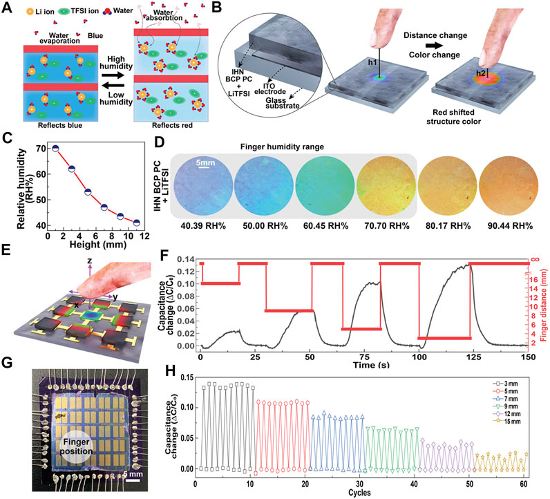
FIGURE 12. 3D touchless BCP structural color-sensing display. (A) Schematic illustration of humidity-sensitive structure’s color change in an LiTFSI-doped IHN BCP PC. (B) Schematic of two-terminal parallel-type 3D touchless sensing display with an LiTFSI-doped IHN BCP PC. (C) Variation of RH as a function of finger-to-PC distance. (D) Photographs of an LiTFSI-doped IHN BCP PCs in various RH conditions from ∼40 to 90% RH. (E) Schematic and (G) photograph of arrays for 3D touchless sensing displays. (F) Capacitance change of a 3D touchless sensing display with an LiTFSI-doped IHN BCP PC upon the variation of finger-to-PC distance from 15, 9, 5, and 3 mm. (H) Variation in the capacitance of the 3D touchless sensing display upon repetitive alteration of the finger-to-PC distance. The figure is reprinted with permission from Kang et al. (2020), copyright 2020, AAAS.
In summary, BCP self-assembly easily constructs regular nanostructure arrays at a low cost for sensor applications, such as environmental monitoring and disease diagnoses.
Ultrafiltration Membranes
Ultrafiltration membranes have attracted much interest due to their significant merits, such as convenient operation, low power consumption, and high separation efficiency (Hampu et al., 2020). Currently, they are widely used for water treatment, solution concentration, and chemical separation (Hampu et al., 2020; Guo et al., 2021). However, conventional membranes have some fatal drawbacks, such as a broad pore-size distribution that is not conducive to precise separation and easy fouling because of tortuous and dead-angle channels in the membrane (Hampu et al., 2020). Comparatively, isoporous membranes possess unique features such as straight nanochannels and monodisperse pores. BCP templating can readily construct isoporous membranes at a low cost, which makes it one of the most attractive approaches for fabricating ultrafiltration membranes. To date, there are numerous reports about the use of BCP self-assembly to prepare ultrafiltration membranes, which have been extensively applied in the chemical industry, food production, environmental studies, and biomedicine (Jackson and Hillmyer, 2010; Werber et al., 2016; Greil et al., 2017; John et al., 2021).
For example, a mixture of PS-b-PMMA and homopolymer PMMA was self-assembled on a substrate to fabricate nanoporous membranes with a pore size of 15 nm (Yang et al., 2006). The nanoporous membranes showed both ultrahigh selectivity and flux for the filtration of viruses such as human rhinovirus type 14. Yang et al. (2010) successfully fabricated a novel drug delivery device by BCP templating. The self-assembly of cylinder-forming PS-b-PMMA was used to form a nanoporous membrane with cylindrical nanochannels, and then a gold film was deposited on the nanoporous membrane to accurately govern the pore size down to 6 nm. Based on the drug-delivery nanodevice, a zero-order release of bovine serum albumin (BSA) and human growth hormone was achieved via single-file diffusion, and the excellent performance could be sustained for two months. Moreover, the device was implanted in rats that continued to release nearly constant growth hormone for three weeks, demonstrating the feasibility of long-term controlled administration of therapeutic protein drugs. Hahn et al. (2014) prepared four different PS-b-P4VP membranes with pore sizes ranging from 17 to 53 nm via BCP self-assembly. The results demonstrated that the 23-nm pore-size membrane has the best separation performance for myoglobin and ferritin, and the separation selectivity was up to 27.
A nanoporous alumina ultrafiltration membrane was manufactured by employing cylinder-forming PS-b-PMMA with PS cylinders (Zhou et al., 2017). The detailed preparation process flow is shown in Figure 13. PS-b-PMMA films underwent self-assembly on a random copolymer mat on the top of a layer of a water-soluble sodium salt of poly(acrylic acid) (PAA). The random copolymer mat and BCP films were floated off in water and then were transferred onto a commercial anodic aluminum oxide (AAO)-supporting membrane. AlOx was selectively deposited in the PMMA matrix with an SIS technique. The hybrid BCP–AlOx film was etched to remove the BCP, and a nanoporous AlOx membrane with a narrow pore size distribution was fabricated. The BCP soft templates were changed into AlOx hard templates by the SIS process. The use of the well-ordered nanoporous AlOx membrane as an ultrafiltration device successfully realized protein separation with high flux and high selectivity. A separation factor of 7.7 was obtained for BSA and bovine hemoglobin. At the same pore size, the ultrafiltration performance of a nanoporous AlOx membrane exceeded common commercial nanoporous membranes, such as AAO membranes. In addition, an isoporous membrane with a pore size of sub-10 nm and pore density 1.3 × 10¹⁵/m2 was fabricated through the self-assembly of cylinder-forming PS-b-P4VP for protein separation (Zhu et al., 2018).
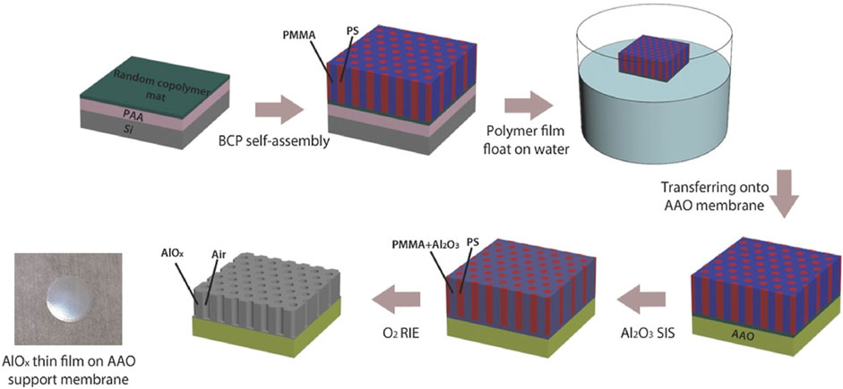
FIGURE 13. Schematic illustration of BCP-templated AlOx membrane fabrication process. The figure is reprinted with permission from Zhou et al. (2017), copyright 2017, Wiley-VCH.
For water purification, polystyrene-block-polylactide (PS-b-PLA) was used to construct nanoporous membranes with monodisperse pores of 24 nm diameter (Phillip et al., 2010). PS-b-PLA was cast onto a microporous membrane, which offered mechanical reinforcement to yield a 4-μm thin film. By choosing appropriate casting solvents and controlling the solvent evaporation rate, a thin film with a vertically oriented PLA cylinder in the PS matrix was generated. Then, the PLA domains were completely removed through wet etching, resulting in a nanoporous PS film. The nanoporous membranes as water filtration membranes had a pure water permeability of 1.15 L/(m2hbar). Rejection increased with the solute molecular weight, and the rejection of the 100 kg/mol PEO sample was nearly complete (>93%). Querelle et al. (2013) fabricated ultrafiltration membranes with pores of 20 nm diameter by employing a polystyrene-block-polyisoprene-block-polylactide (PS-b-PI-b-PLA) self-assembly template. The structure of the BCP template was a core (PLA)–cylindrical shell (PI)–matrix (PS). The added PI block was used to improve the mechanical strength of the PS film. The PLA cylinders were removed to form an ultrafiltration membrane that displayed an excellent hydraulic permeability of 165 L/(m2 h bar) and could size-discriminate PEO solutes. In-plane aligned nanostructures were prepared as ultrafiltration membranes with uniform slit pores through the self-assembly of PS-b-P2VP (Guo and Wang, 2014). The fabricated membranes were endowed with an ultrahigh water flux and sharp selectivity. Based on the self-assembly of polyarylester-block-polydimethylsiloxane (PAR-b-PDMS), a superhydrophobic and superoleophilic porous membrane was fabricated by using a spraying-coating process to realize oil–water separation (Li et al., 2016). A 100-nm-thick isoporous membrane with a 23-nm pore size was generated by the self-assembly of PS-b-PMMA (Luo et al., 2020). It severed as an ultrafiltration membrane for effective oil–water separation.
In recent years, a novel concept of a multifunctional ultrafiltration membrane has been developed. For example, polystyrene-block-poly(4-vinylpyridine)-block-poly(propylene sulfide) (PS-b-P4VP-b-PPS) has been self-assembled to generate isoporous ultrafiltration membranes where the PPS block serves as a functional layer that is linked to the pore walls (Zhang et al., 2016). The new architecture of isoporous membranes can be employed not only as an ultrafiltration membrane to separate and purify molecules but also as a sensor for identifying target molecules. In addition, the surface of the pore wall can also be decorated with amines or carboxylic groups instead of sulfhydryl groups to add a multifunctional capability to the isoporous membranes. Therefore, the work has paved the way for manufacturing multifunctional nanodevices for sensing and separation. An isoporous membrane with tuning pore size has been generated with PS-b-P4VP templates, which have been used to separate the cationic dye methylene blue from the aqueous solution (Zhang et al., 2019). The membrane’s pore size is controllable from ultrafiltration to nanofiltration by quaternizing the P4VP block. Subsequently, they have also fabricated an isoporous membrane which exhibited an excellent separation selectivity for the small molecules with 1–2 nm lateral dimensions (Zhang et al., 2020).
Generally, the BCP self-assembly offers a platform to obtain isoporous membranes with adjustable pore sizes in the range of 10–50 nm. It is one of the most promising approaches to manufacture ultrafiltration membranes on a large scale.
Conclusion
Today, the market requirement for faster, smaller, stronger, and more energy-efficient nanodevices greatly facilitates the development of nanofabrication techniques. BCP self-assembly has emerged as a novel nanopatterning technique that is widely used in manufacturing advanced nanodevices. The technique relies on molecular self-assembly to yield organized nanostructure arrays with high resolution and can surpass the diffraction limit of conventional photolithography. Additionally, BCP self-assembly is endowed with many significant merits, such as high throughput, high efficiency, good compatibility, excellent scalability, low cost, and process simplicity.
In this review, we systematically summarize the use of BCP self-assembly to generate highly versatile templates for use in manufacturing nanodevices. For memory nanodevices, BCP templates can be used as the functional structure of the device and can also serve as masks for further patterning. Additionally, the morphologies and orientations of the nanostructures based on BCP self-assembly can determine the properties of nonvolatile memory. In the fabrication of BPM, BCP templating can readily construct bit patterns with a density that surpasses 1.5 Tb/in2, thanks to its high resolution and simple process. In the next few years, BCP self-assembly may be mainly employed in the fabrication of high-resolution NIL templates for BPM patterning. In the manufacturing of FinFET, an 11.2-nm fin structure can be fabricated by employing BCP self-assembly on a 300-mm pilot line. Furthermore, BCP templating has become a very promising technique for the practical preparation of sub-10 nm fin structures with low-line edge roughness and low-line width roughness at a low cost. For photonic nanodevices, BCP self-assembly permits the formation of ordered 2D and 3D nanostructures with controlled periodicity and orientation on a large scale, providing a simple, rapid, and cost-effective fabrication approach for new functional optical materials. In the fabrication of solar cells, conjugated BCPs can directly build high-performance photovoltaic devices by controlling their compositions, nanoscale morphologies, and orientations. In the preparation of sensors, BCP templates are adapted for creating organized nanostructure arrays as sensors for detecting gas, ethanol, sugar, protein, humidity, solvatochromic materials, and strains. For ultrafiltration membranes, BCP templating can easily construct ultra large-area isoporous membranes with a tunable pore size for water purification, protein separation, and drug delivery.
In short, creating cutting-edge nanodevices in demand today is extremely challenging, which requires uniting with experts from different fields and working together to continuously innovate and deliver feasible solutions. Fortunately, BCP self-assembly as a bottom-up technique has displayed a tremendous promise for manufacturing sophisticated nanodevices. We hope that this review can provide inspiration for scientists who intend to further expand the applications of BCP self-assembly.
Author Contributions
XH designed and wrote the manuscript. SX supervised this work. All authors have approved it for publication.
Funding
This work was financially supported by the National Natural Science Foundation of China (No. 61974030).
Conflict of Interest
The authors declare that the research was conducted in the absence of any commercial or financial relationships that could be construed as a potential conflict of interest.
Publisher’s Note
All claims expressed in this article are solely those of the authors and do not necessarily represent those of their affiliated organizations, or those of the publisher, the editors, and the reviewers. Any product that may be evaluated in this article, or claim that may be made by its manufacturer, is not guaranteed or endorsed by the publisher.
References
Alvarez‐Fernandez, A., Cummins, C., Saba, M., Steiner, U., Fleury, G., Ponsinet, V., et al. (2021). Block Copolymer Directed Metamaterials and Metasurfaces for Novel Optical Devices. Adv. Opt. Mater. 9, 2100175. doi:10.1002/adom.202100175
Alvarez-Fernandez, A., Fleury, G., Ponsinet, V., Walmsness, P. M., and Kildemo, M. (2020). Formation and Optical Response of Self-Assembled Gold Nanoparticle Lattices on Oxidized Silicon Synthesized Using Block Copolymers. J. Vac. Sci. Technol. B 38, 013601. doi:10.1116/1.5129667
Ayyub, O. B., Sekowski, J. W., Yang, T.-I., Zhang, X., Briber, R. M., and Kofinas, P. (2011). Color Changing Block Copolymer Films for Chemical Sensing of Simple Sugars. Biosens. Bioelectron. 28, 349–354. doi:10.1016/j.bios.2011.07.043
Ayyub, O. B., Ibrahim, M. B., Briber, R. M., and Kofinas, P. (2013). Self-assembled Block Copolymer Photonic Crystal for Selective Fructose Detection. Biosens. Bioelectron. 46, 124–129. doi:10.1016/j.bios.2013.02.025
Azuma, K., Sun, J., Choo, Y., Rokhlenko, Y., Dwyer, J. H., Schweitzer, B., et al. (2018). Self-Assembly of an Ultrahigh-χ Block Copolymer with Versatile Etch Selectivity. Macromolecules 51, 6460–6467. doi:10.1021/acs.macromol.8b01409
Barcelo, S., and Li, Z. (2016). Nanoimprint Lithography for Nanodevice Fabrication. Nano Converg. 3, 21. doi:10.1186/s40580-016-0081-y
Bates, F. S., and Fredrickson, G. H. (1990). Block Copolymer Thermodynamics: Theory and Experiment. Annu. Rev. Phys. Chem. 41, 525–557. doi:10.1146/annurev.pc.41.100190.002521
Black, C. T. (2005). Self-aligned Self Assembly of Multi-Nanowire Silicon Field Effect Transistors. Appl. Phys. Lett. 87, 163116. doi:10.1063/1.2112191
Botiz, I., and Darling, S. B. (2009). Self-Assembly of Poly(3-hexylthiophene)-block-Polylactide Block Copolymer and Subsequent Incorporation of Electron Acceptor Material. Macromolecules 42, 8211–8217. doi:10.1021/ma901420h
Cerba, T., Hauchecorne, P., Martin, M., Moeyaert, J., Alcotte, R., Salem, B., et al. (2019). InAs/GaSb Thin Layers Directly Grown on Nominal (001)-Si Substrate by MOVPE for the Fabrication of InAs FINFET. J. Cryst. Growth 510, 18–22. doi:10.1016/j.jcrysgro.2018.12.014
Chang, Y. H., Ku, C. W., Zhang, Y. H., Wang, H. C., and Chen, J. Y. (2020). Ultrafast Responsive Non‐Volatile Flash Photomemory via Spatially Addressable Perovskite/Block Copolymer Composite Film. Adv. Funct. Mater. 30, 2000764. doi:10.1002/adfm.202000764
Chen, C.-M., Liu, C.-M., Wei, K.-H., Jeng, U.-S., and Su, C.-H. (2012). Non-volatile Organic Field-Effect Transistor Memory Comprising Sequestered Metal Nanoparticles in a Diblock Copolymer Film. J. Mater. Chem. 22, 454–461. doi:10.1039/C1JM13936C
Chen, J.-C., Liu, C.-L., Sun, Y.-S., Tung, S.-H., and Chen, W.-C. (2012). Tunable Electrical Memory Characteristics by the Morphology of Self-Assembled Block Copolymers:PCBM Nanocomposite Films. Soft Matter 8, 526–535. doi:10.1039/C1SM06622F
Chen, Y.-C., Lin, Y.-C., Hsieh, H.-C., Hsu, L.-C., Yang, W.-C., Isono, T., et al. (2021). Improving the Performance of Photonic Transistor Memory Devices Using Conjugated Block Copolymers as a Floating Gate. J. Mater. Chem. C 9, 1259–1268. doi:10.1039/D0TC05326K
Chen, C.-M., Liu, C.-M., Wei, K.-H., Jeng, U. S., and Su, C.-H. (2012). Non-volatile Organic Field-effect Transistor Memory Comprising Sequestered Metal Nanoparticles in a Diblock Copolymer Film. J. Mater. Chem. 22, 454–461. doi:10.1039/C1JM13936C
Chen, Y. (2015). Nanofabrication by Electron Beam Lithography and Its Applications: A Review. Microelectronic Eng. 135, 57–72. doi:10.1016/j.mee.2015.02.042
Chen, Y., Shu, Z., Zhang, S., Zeng, P., Liang, H., Zheng, M., et al. (2021). Sub-10 nm Fabrication: Methods and Applications. Int. J. Extrem. Manuf. 3, 032002. doi:10.1088/2631-7990/ac087c
Chen, Y., and Xiong, S. (2020). Directed Self-Assembly of Block Copolymers for Sub-10 nm Fabrication. Int. J. Extrem. Manuf. 2, 032006. doi:10.1088/2631-7990/aba3ae
Cheng, J. Y., Ross, C. A., Chan, V. Z.-H., Thomas, E. L., Lammertink, R. G. H., and Vancso, G. J. (2001). Formation of a Cobalt Magnetic Dot Array via Block Copolymer Lithography. Adv. Mater. 13, 1174–1178. doi:10.1002/1521-4095(200108)13:15<1174:AID-ADMA1174>3.0.CO;2-Q
Chuang, T.-H., Chiang, Y.-C., Hsieh, H.-C., Isono, T., Huang, C.-W., Borsali, R., et al. (2020). Nanostructure- and Orientation-Controlled Resistive Memory Behaviors of Carbohydrate-block-Polystyrene with Different Molecular Weights via Solvent Annealing. ACS Appl. Mater. Inter. 12, 23217–23224. doi:10.1021/acsami.0c04551
Chung, S.-W., Ginger, D. S., Morales, M. W., Zhang, Z., Chandrasekhar, V., Ratner, M. A., et al. (2005). Top-Down Meets Bottom-Up: Dip-Pen Nanolithography and DNA-Directed Assembly of Nanoscale Electrical Circuits. Small 1, 64–69. doi:10.1002/smll.200400005
Crossland, E. J. W., Kamperman, M., Nedelcu, M., Ducati, C., Wiesner, U., Smilgies, D.-M., et al. (2009). A Bicontinuous Double Gyroid Hybrid Solar Cell. Nano Lett. 9, 2807–2812. doi:10.1021/nl803174p
Cummins, C., and Morris, M. A. (2018). Using Block Copolymers as Infiltration Sites for Development of Future Nanoelectronic Devices: Achievements, Barriers, and Opportunities. Microelectronic Eng. 195, 74–85. doi:10.1016/j.mee.2018.04.005
Cushen, J. D., Bates, C. M., Rausch, E. L., Dean, L. M., Zhou, S. X., Willson, C. G., et al. (2012). Thin Film Self-Assembly of Poly(trimethylsilylstyrene-b-D,L-lactide) with Sub-10 nm Domains. Macromolecules 45, 8722–8728. doi:10.1021/ma301238j
Darling, S. B. (2009). Block Copolymers for Photovoltaics. Energy Environ. Sci. 2, 1266–1273. doi:10.1039/B912086F
Doerk, G. S., Gao, H., Wan, L., Lille, J., Patel, K. C., Chapuis, Y.-A., et al. (2015). Transfer of Self-Aligned Spacer Patterns for Single-Digit Nanofabrication. Nanotechnology 26, 085304. doi:10.1088/0957-4484/26/8/085304
Feynman, R. P. (1959). “There’s Plenty of Room at the Bottom,” in APS Annual Meetings, California, December 29, 1959, 22–36.
Fourkas, J. T., Gao, J., Han, Z., Liu, H., Marmiroli, B., Naughton, M. J., et al. (2021). Grand Challenges in Nanofabrication: There Remains Plenty of Room at the Bottom. Front. Nanotechnol. 3, 700849. doi:10.3389/fnano.2021.700849
Frascaroli, J., Brivio, S., Ferrarese Lupi, F., Seguini, G., Boarino, L., Perego, M., et al. (2015). Resistive Switching in High-Density Nanodevices Fabricated by Block Copolymer Self-Assembly. ACS Nano 9, 2518–2529. doi:10.1021/nn505131b
Gao, D., Hollinger, J., and Seferos, D. S. (2012). Selenophene-thiophene Block Copolymer Solar Cells with Thermostable Nanostructures. ACS Nano 6, 7114–7121. doi:10.1021/nn3021844
Greil, S., Rahman, A., Liu, M., and Black, C. T. (2017). Gas Transport Selectivity of Ultrathin, Nanoporous, Inorganic Membranes Made from Block Copolymer Templates. Chem. Mater. 29, 9572–9578. doi:10.1021/acs.chemmater.7b04174
Griffiths, R. A., Williams, A., Oakland, C., Roberts, J., Vijayaraghavan, A., and Thomson, T. (2013). Directed Self-Assembly of Block Copolymers for Use in Bit Patterned Media Fabrication. J. Phys. D: Appl. Phys. 46, 503001. doi:10.1088/0022-3727/46/50/503001
Guarini, K. W., Black, C. T., Zhang, Y., Babich, I. V., Sikorski, E. M., and Gignac, L. M. (2003). “Low Voltage, Scalable Nanocrystal Flash Memory Fabricated by Templated Self Assembly,” in IEEE International Electron Devices Meeting 2003, Washington, DC, December 8–10, 2003, 541–544. doi:10.1109/IEDM.2003.1269340
Guldin, S., Kohn, P., Stefik, M., Song, J., Divitini, G., Ecarla, F., et al. (2013). Self-cleaning Antireflective Optical Coatings. Nano Lett. 13, 5329–5335. doi:10.1021/nl402832u
Guo, C., Lin, Y. H., Witman, M. D., Smith, K. A., Wang, C., Hexemer, A., et al. (2013). Conjugated Block Copolymer Photovoltaics with Near 3% Efficiency through Microphase Separation. Nano Lett. 13, 2957–2963. doi:10.1021/nl401420s
Guo, L., and Wang, Y. (2014). Nanoslitting of Phase-Separated Block Copolymers by Solvent Swelling for Membranes with Ultrahigh Flux and Sharp Selectivity. Chem. Commun. 50, 12022–12025. doi:10.1039/C4CC05009F
Guo, L., and Wang, Y. (2018). Retarded Evaporation-Induced Synthesis of Lamellar Block Copolymer Supramolecules for Solvatochromic Sensing. Sensors Actuators B: Chem. 277, 172–178. doi:10.1016/j.snb.2018.08.158
Guo, L., Wang, Y., and Steinhart, M. (2021). Porous Block Copolymer Separation Membranes for 21st Century Sanitation and Hygiene. Chem. Soc. Rev. 50, 6333–6348. doi:10.1039/D0CS00500B
Guo, L., Zhong, Z., and Wang, Y. (2016). Atomic Layer Deposition on Block Copolymer Membranes with Gyroidal Nanopores toward Periodically Nanostructured Vapor Sensors: Nanotubes versus Nanorods. Adv. Mater. Inter. 3, 1600017. doi:10.1002/admi.201600017
Hahn, J., Clodt, J. I., Filiz, V., and Abetz, V. (2014). Protein Separation Performance of Self-Assembled Block Copolymer Membranes. RSC Adv. 4, 10252–10260. doi:10.1039/C3RA47306F
Hampu, N., Werber, J. R., Chan, W. Y., Feinberg, E. C., and Hillmyer, M. A. (2020). Next-Generation Ultrafiltration Membranes Enabled by Block Polymers. ACS Nano 14, 16446–16471. doi:10.1021/acsnano.0c07883
He, M., Han, W., Ge, J., Yang, Y., Qiu, F., and Lin, Z. (2011). All-conjugated Poly(3-alkylthiophene) Diblock Copolymer-Based Bulk Heterojunction Solar Cells with Controlled Molecular Organization and Nanoscale Morphology. Energ. Environ. Sci. 4, 2894–2902. doi:10.1039/C1EE01509E
Hobbs, R. G., Petkov, N., and Holmes, J. D. (2012). Semiconductor Nanowire Fabrication by Bottom-Up and Top-Down Paradigms. Chem. Mater. 24, 1975–1991. doi:10.1021/cm300570n
Hoheisel, T. N., Hur, K., and Wiesner, U. B. (2015). Block Copolymer-Nanoparticle Hybrid Self-Assembly. Prog. Polym. Sci. 40, 3–32. doi:10.1016/j.progpolymsci.2014.10.002
Hong, A. J., Liu, C.-C., Wang, Y., Kim, J., Xiu, F., Ji, S., et al. (2010). Metal Nanodot Memory by Self-Assembled Block Copolymer Lift-Off. Nano Lett. 10, 224–229. doi:10.1021/nl903340a
Hsu, L.-C., Isono, T., Lin, Y.-C., Kobayashi, S., Chiang, Y.-C., Jiang, D.-H., et al. (2021). Stretchable OFET Memories: Tuning the Morphology and the Charge-Trapping Ability of Conjugated Block Copolymers through Soft Segment Branching. ACS Appl. Mater. Inter. 13, 2932–2943. doi:10.1021/acsami.0c18820
Hu, X.-H., and Xiong, S.-S. (2021). Advanced Lithography: Directed Self-Assembly. Chin. J. Appl. Chem. 38, 1029–1078. doi:10.19894/j.issn.1000-0518.210278
Hu, X., An, X., and Li, L. (2016). Easy Synthesis of Highly Fluorescent Carbon Dots from Albumin and Their Photoluminescent Mechanism and Biological Imaging Applications. Mater. Sci. Eng. C 58, 730–736. doi:10.1016/j.msec.2015.09.066
Hulkkonen, H. H., Salminen, T., and Niemi, T. (2017). Block Copolymer Patterning for Creating Porous Silicon Thin Films with Tunable Refractive Indices. ACS Appl. Mater. Inter. 9, 31260–31265. doi:10.1021/acsami.6b16110
Hulkkonen, H., Sah, A., and Niemi, T. (2018). All-metal Broadband Optical Absorbers Based on Block Copolymer Nanolithography. ACS Appl. Mater. Inter. 10, 42941–42947. doi:10.1021/acsami.8b17294
Hung, C.-C., Chiu, Y.-C., Wu, H.-C., Lu, C., Bouilhac, C., Otsuka, I., et al. (2017). Conception of Stretchable Resistive Memory Devices Based on Nanostructure-Controlled Carbohydrate-block-Polyisoprene Block Copolymers. Adv. Funct. Mater. 27, 1606161. doi:10.1002/adfm.201606161
Hung, C.-C., Nakahira, S., Chiu, Y.-C., Isono, T., Wu, H.-C., Watanabe, K., et al. (2018). Control over Molecular Architectures of Carbohydrate-Based Block Copolymers for Stretchable Electrical Memory Devices. Macromolecules 51, 4966–4975. doi:10.1021/acs.macromol.8b00874
Idriss, H., Gapin, A., Khelifi, W., Blanc, S., Karamé, I., Chambon, S., et al. (2020). Complementary Absorption versus Morphology in All-Conjugated Block Copolymer Solar Cells. Macromolecules 53, 9043–9053. doi:10.1021/acs.macromol.0c01680
Jackson, E. A., and Hillmyer, M. A. (2010). Nanoporous Membranes Derived from Block Copolymers: From Drug Delivery to Water Filtration. ACS Nano 4, 3548–3553. doi:10.1021/nn1014006
Jeong, C. K., Jin, H. M., Ahn, J.-H., Park, T. J., Yoo, H. G., Koo, M., et al. (2014). Electrical Biomolecule Detection Using Nanopatterned Silicon via Block Copolymer Lithography. Small 10, 337–343. doi:10.1002/smll.201301202
Jeong, G., Yu, D. M., Mapas, J. K. D., Sun, Z., Rzayev, J., and Russell, T. P. (2017). Realizing 5.4 nm Full Pitch Lamellar Microdomains by a Solid-State Transformation. Macromolecules 50, 7148–7154. doi:10.1021/acs.macromol.7b01443
Ji, S., Wan, L., Liu, C.-C., and Nealey, P. F. (2016). Directed Self-Assembly of Block Copolymers on Chemical Patterns: A Platform for Nanofabrication. Prog. Polym. Sci. 54-55, 76–127. doi:10.1016/j.progpolymsci.2015.10.006
Jin, H. M., Kim, J. Y., Heo, M., Jeong, S.-J., Kim, B. H., Cha, S. K., et al. (2018). Ultralarge Area Sub-10 nm Plasmonic Nanogap Array by Block Copolymer Self-Assembly for Reliable High-Sensitivity SERS. ACS Appl. Mater. Inter. 10, 44660–44667. doi:10.1021/acsami.8b17325
John, R., Pal, K., Jayan, J. S., Appukuttan, S., and Joseph, K. (2021). New Emerging Review on Advances in Block Copolymer Based Water Purification Membranes. J. Mol. Struct. 1231, 129926. doi:10.1016/j.molstruc.2021.129926
Jung, Y. S., Jung, W., Tuller, H. L., and Ross, C. A. (2008). Nanowire Conductive Polymer Gas Sensor Patterned Using Self-Assembled Block Copolymer Lithography. Nano Lett. 8, 3776–3780. doi:10.1021/nl802099k
Kang, H. S., Han, S. W., Park, C., Lee, S. W., Eoh, H., Baek, J., et al. (2020). 3D Touchless Multiorder Reflection Structural Color Sensing Display. Sci. Adv. 6, eabb5769. doi:10.1126/sciadv.abb5769
Kang, Y. (2012). Colorimetric Humidity Sensors Based on Block Copolymer Photonic Gels. Macromol. Res. 20, 1223–1225. doi:10.1007/s13233-012-0202-3
Khawas, K., Daripa, S., Kumari, P., and Kuila, B. K. (2018). Electrochemical and Electronic Properties of Transparent Coating from Highly Solution Processable Graphene Using Block Copolymer Supramolecular Assembly: Application toward Metal Ion Sensing and Resistive Switching Memory. ACS Omega 3, 7106–7116. doi:10.1021/acsomega.8b00883
Kim, J., and Franco, E. (2020). RNA Nanotechnology in Synthetic Biology. Curr. Opin. Biotechnol. 63, 135–141. doi:10.1016/j.copbio.2019.12.016
Kim, J. Y., Kim, H., Kim, B. H., Chang, T., Lim, J., Jin, H. M., et al. (2016). Highly Tunable Refractive Index Visible-Light Metasurface from Block Copolymer Self-Assembly. Nat. Commun. 7, 12911. doi:10.1038/ncomms12911
Kirschner, J., Will, J., Rejek, T. J., Portilla, L., Berlinghof, M., Schweizer, P., et al. (2017). Memory Effect of Self-Assembled PS-b-PEO Block Copolymer Films with Selectively Embedded Functionalized TiO2 Nanoparticles. Adv. Mater. Inter. 4, 1700230. doi:10.1002/admi.201700230
Kwak, J., Mishra, A. K., Lee, J., Lee, K. S., Choi, C., Maiti, S., et al. (2017). Fabrication of Sub-3 nm Feature Size Based on Block Copolymer Self-Assembly for Next-Generation Nanolithography. Macromolecules 50, 6813–6818. doi:10.1021/acs.macromol.7b00945
Lee, Y.-H., Chen, W.-C., Chiang, C.-J., Kau, K.-C., Liou, W.-S., Lee, Y.-P., et al. (2015). A New Strategy for Fabricating Organic Photovoltaic Devices with Stable D/A Double-Channel Network to Enhance Performance Using Self-Assembling All-Conjugated Diblock Copolymer. Nano Energy 13, 103–116. doi:10.1016/j.nanoen.2015.01.022
Leong, W. L., Lee, P. S., Lohani, A., Lam, Y. M., Chen, T., Zhang, S., et al. (2008). Non-volatile Organic Memory Applications Enabled by In Situ Synthesis of Gold Nanoparticles in a Self-Assembled Block Copolymer. Adv. Mater. 20, 2325–2331. doi:10.1002/adma.200702567
Levinson, H. J., and Brunner, T. A. (2018). Current Challenges and Opportunities for EUV Lithography. Proc. SPIE 10809, 1080903. doi:10.1117/12.2502791
Li, C., Li, Q., Kaneti, Y. V., Hou, D., Yamauchi, Y., and Mai, Y. (2020). Self-assembly of Block Copolymers towards Mesoporous Materials for Energy Storage and Conversion Systems. Chem. Soc. Rev. 49, 4681–4736. doi:10.1039/D0CS00021C
Li, H., Zhao, X., Wu, P., Zhang, S., and Geng, B. (2016). Facile Preparation of Superhydrophobic and Superoleophilic Porous Polymer Membranes for Oil/Water Separation from a Polyarylester Polydimethylsiloxane Block Copolymer. J. Mater. Sci. 51, 3211–3218. doi:10.1007/s10853-015-9632-6
Lindner, S. M., Hüttner, S., Chiche, A., Thelakkat, M., and Krausch, G. (2006). Charge Separation at Self-Assembled Nanostructured Bulk Interface in Block Copolymers. Angew. Chem. Int. Ed. 45, 3364–3368. doi:10.1002/anie.200503958
Lindner, S. M., and Thelakkat, M. (2004). Nanostructures of n-Type Organic Semiconductor in a p-Type Matrix via Self-Assembly of Block Copolymers. Macromolecules 37, 8832–8835. doi:10.1021/ma0481656
Liu, C.-C. C., Franke, E., Lie, F. L., Sieg, S., Tsai, H., Lai, K., et al. (2016). DSA Patterning Options for FinFET Formation at 7nm Node. Proc. SPIE 9777, 97770R. doi:10.1117/12.2219670
Liu, C.-C., Franke, E., Mignot, Y., Xie, R., Yeung, C. W., Zhang, J., et al. (2018). Directed Self-Assembly of Block Copolymers for 7 Nanometre FinFET Technology and beyond. Nat. Electron. 1, 562–569. doi:10.1038/s41928-018-0147-4
Luo, Y., Wang, X., Zhang, R., Singh, M., Ammar, A., Cousins, D., et al. (2020). Vertically Oriented Nanoporous Block Copolymer Membranes for Oil/Water Separation and Filtration. Soft Matter 16, 9648–9654. doi:10.1039/D0SM00526F
Mansky, P., haikin, P., and Thomas, E. L. (1995). Monolayer Films of Diblock Copolymer Microdomains for Nanolithographic Applications. J. Mater. Sci. 30, 1987–1992. doi:10.1007/BF00353023
Mansky, P., Russell, T. P., Hawker, C. J., Pitsikalis, M., and Mays, J. (1997). Ordered Diblock Copolymer Films on Random Copolymer Brushes. Macromolecules 30, 6810–6813. doi:10.1021/ma970675v
Mokarian-Tabari, P., Senthamaraikannan, R., Glynn, C., Collins, T. W., Cummins, C., Nugent, D., et al. (2017). Large Block Copolymer Self-Assembly for Fabrication of Subwavelength Nanostructures for Applications in Optics. Nano Lett. 17, 2973–2978. doi:10.1021/acs.nanolett.7b00226
Mullen, E., and Morris, M. A. (2021). Green Nanofabrication Opportunities in the Semiconductor Industry: A Life Cycle Perspective. Nanomaterials 11, 1085. doi:10.3390/nano11051085
Mun, B. H., You, B. K., Yang, S. R., Yoo, H. G., Kim, J. M., Park, W. I., et al. (2015). Flexible One Diode-One Phase Change Memory Array Enabled by Block Copolymer Self-Assembly. ACS Nano 9, 4120–4128. doi:10.1021/acsnano.5b00230
Omidian, M., Leitherer, S., Néel, N., Brandbyge, M., and Kröger, J. (2021). Electric-Field Control of a Single-Atom Polar Bond. Phys. Rev. Lett. 126, 216801. doi:10.1103/PhysRevLett.126.216801
Owen, A. G., Su, H., Montgomery, A., and Gupta, S. (2017). Comparison of Air and Heptane Solvent Annealing of Block Copolymers for Bit-Patterned Media. J. Vac. Sci. Technol. B 35, 061801. doi:10.1116/1.5004150
Päivänranta, B., Langner, A., Kirk, E., David, C., and Ekinci, Y. (2011). Sub-10 nm Patterning Using EUV Interference Lithography. Nanotechnology 22, 375302. doi:10.1088/0957-4484/22/37/375302
Pan, D. Z. (2018). Directed Self-Assembly for Advanced Chips. Nat. Electron. 1, 530–531. doi:10.1038/s41928-018-0152-7
Park, S., Lee, D. H., Xu, J., Kim, B., Hong, S. W., Jeong, U., et al. (2009). Macroscopic 10-Terabit-Per-Square-Inch Arrays from Block Copolymers with Lateral Order. Science 323, 1030–1033. doi:10.1126/science.1168108
Park, T. H., Yu, S., Cho, S. H., Kang, H. S., Kim, Y., Kim, M. J., et al. (2018). Block Copolymer Structural Color Strain Sensor. NPG Asia Mater. 10, 328–339. doi:10.1038/s41427-018-0036-3
Park, W. I., Yoon, J. M., Park, M., Lee, J., Kim, S. K., Jeong, J. W., et al. (2012). Self-assembly-induced Formation of High-Density Silicon Oxide Memristor Nanostructures on Graphene and Metal Electrodes. Nano Lett. 12, 1235–1240. doi:10.1021/nl203597d
Park, W. I., You, B. K., Mun, B. H., Seo, H. K., Lee, J. Y., Hosaka, S., et al. (2013). Self-assembled Incorporation of Modulated Block Copolymer Nanostructures in Phase-Change Memory for Switching Power Reduction. ACS Nano 7, 2651–2658. doi:10.1021/nn4000176
Phillip, W. A., O’Neill, B., Rodwogin, M., Hillmyer, M. A., and Cussler, E. L. (2010). Self-assembled Block Copolymer Thin Films as Water Filtration Membranes. ACS Appl. Mater. Inter. 2, 847–853. doi:10.1021/am900882t
Pinto-Gómez, C., Pérez-Murano, F., Bausells, J., Villanueva, L. G., and Fernández-Regúlez, M. (2020). Directed Self-Assembly of Block Copolymers for the Fabrication of Functional Devices. Polymers 12, 2432. doi:10.3390/polym12102432
Querelle, S. E., Jackson, E. A., Cussler, E. L., and Hillmyer, M. A. (2013). Ultrafiltration Membranes with a Thin Poly(styrene)-b-Poly(isoprene) Selective Layer. ACS Appl. Mater. Inter. 5, 5044–5050. doi:10.1021/am400847m
Rasappa, S., Borah, D., Faulkner, C. C., Lutz, T., Shaw, M. T., Holmes, J. D., et al. (2013). Fabrication of a Sub-10 nm Silicon Nanowire Based Ethanol Sensor Using Block Copolymer Lithography. Nanotechnology 24, 065503. doi:10.1088/0957-4484/24/6/065503
Rasappa, S., Schulte, L., Ndoni, S., and Niemi, T. (2018). Directed Self-Assembly of a High-Chi Block Copolymer for the Fabrication of Optical Nanoresonators. Nanoscale 10, 18306–18314. doi:10.1039/C8NR05831H
Ren, G., Wu, P.-T., and Jenekhe, S. A. (2010). Enhanced Performance of Bulk Heterojunction Solar Cells Using Block Copoly(3-alkylthiophene)s. Chem. Mater. 22, 2020–2026. doi:10.1021/cm903783w
Ruiz, R., Dobisz, E., and Albrecht, T. R. (2011). Rectangular Patterns Using Block Copolymer Directed Assembly for High Bit Aspect Ratio Patterned Media. ACS Nano 5, 79–84. doi:10.1021/nn101561p
Sadegh, F., Akin, S., Moghadam, M., Keshavarzi, R., Mirkhani, V., Ruiz‐Preciado, M. A., et al. (2021). Copolymer‐Templated Nickel Oxide for High‐Efficiency Mesoscopic Perovskite Solar Cells in Inverted Architecture. Adv. Funct. Mater. 31, 2102237. doi:10.1002/adfm.202102237
Salvatore, S., Vignolini, S., Philpott, J., Stefik, M., Wiesner, U., Baumberg, J. J., et al. (2015). A High Transmission Wave-Guide Wire Network Made by Self-Assembly. Nanoscale 7, 1032–1036. doi:10.1039/C4NR04485A
Sanders, D. P. (2010). Advances in Patterning Materials for 193 nm Immersion Lithography. Chem. Rev. 110, 321–360. doi:10.1021/cr900244n
Sarikaya, M., Tamerler, C., Jen, A. K.-Y., Schulten, K., and Baneyx, F. (2003). Molecular Biomimetics: Nanotechnology through Biology. Nat. Mater 2, 577–585. doi:10.1038/nmat964
Sarkar, B., and Alexandridis, P. (2015). Block Copolymer-Nanoparticle Composites: Structure, Functional Properties, and Processing. Prog. Polym. Sci. 40, 33–62. doi:10.1016/j.progpolymsci.2014.10.009
Seo, M.-S., Jeong, I., Park, J.-S., Lee, J., Han, I. K., Lee, W. I., et al. (2016). Vertically Aligned Nanostructured TiO2 Photoelectrodes for High Efficiency Perovskite Solar Cells via a Block Copolymer Template Approach. Nanoscale 8, 11472–11479. doi:10.1039/C6NR01010E
Silva, G. A. (2004). Introduction to Nanotechnology and Its Applications to Medicine. Surg. Neurol. 61, 216–220. doi:10.1016/j.surneu.2003.09.036
Sindhwani, S., and Chan, W. C. W. (2021). Nanotechnology for Modern Medicine: Next Step towards Clinical Translation. J. Intern. Med. 290, 486–498. doi:10.1111/joim.13254
Sotomayor Torres, C. M., Zankovych, S., Seekamp, J., Kam, A. P., Clavijo Cedeño, C., Hoffmann, T., et al. (2003). Nanoimprint Lithography: An Alternative Nanofabrication Approach. Mater. Sci. Eng. C 23, 23–31. doi:10.1016/S0928-4931(02)00221-7
Stefik, M., Guldin, S., Vignolini, S., Wiesner, U., and Steiner, U. (2015). Block Copolymer Self-Assembly for Nanophotonics. Chem. Soc. Rev. 44, 5076–5091. doi:10.1039/C4CS00517A
Sun, Z., Fang, S., and Hu, Y. H. (2020). 3D Graphene Materials: From Understanding to Design and Synthesis Control. Chem. Rev. 120, 10336–10453. doi:10.1021/acs.chemrev.0c00083
Sun, Z., Li, D., Natarajarathinam, A., Su, H., and Gupta, S. (2012). Large Area Patterning of Single Magnetic Domains with Assistance of Ion Irradiation in Ion Milling. J. Vac. Sci. Technol. B 30, 031803. doi:10.1116/1.4706893
Taniguchi, N. (1974). “On the Basic Concept of Nano-Technology,” in Proc. Int. Cong. Prod. Eng., Tokyo, August 26–29, 1974, 18–23.
Topham, P. D., Parnell, A. J., and Hiorns, R. C. (2011). Block Copolymer Strategies for Solar Cell Technology. J. Polym. Sci. B Polym. Phys. 49, 1131–1156. doi:10.1002/polb.22302
Tsai, H., Miyazoe, H., Vora, A., Magbitang, T., Arellano, N., Liu, C.-C., et al. (2016). High Chi Block Copolymer DSA to Improve Pattern Quality for FinFET Device Fabrication. Proc. SPIE 9779, 977910. doi:10.1117/12.2219544
Tsai, H., Pitera, J. W., Miyazoe, H., Bangsaruntip, S., Engelmann, S. U., Liu, C.-C., et al. (2014). Two-dimensional Pattern Formation Using Graphoepitaxy of PS-b-PMMA Block Copolymers for Advanced FinFET Device and Circuit Fabrication. ACS Nano 8, 5227–5232. doi:10.1021/nn501300b
Vignolini, S., Yufa, N. A., Cunha, P. S., Guldin, S., Rushkin, I., Stefik, M., et al. (2012). A 3D Optical Metamaterial Made by Self-Assembly. Adv. Mater. 24, OP23–OP27. doi:10.1002/adma.201103610
Wan, L., Ruiz, R., Gao, H., Patel, K. C., Lille, J., Zeltzer, G., et al. (2012). Fabrication of Templates with Rectangular Bits on Circular Tracks by Combining Block Copolymer Directed Self-Assembly and Nanoimprint Lithography. Proc. SPIE. 8323, 832319. doi:10.1117/12.916592
Werber, J. R., Osuji, C. O., and Elimelech, M. (2016). Materials for Next-Generation Desalination and Water Purification Membranes. Nat. Rev. Mater. 1, 16018. doi:10.1038/natrevmats.2016.18
Whitesides, G. M. (2005). Nanoscience, Nanotechnology, and Chemistry. Small 1, 172–179. doi:10.1002/smll.200400130
Xiao, S., Yang, X., Edwards, E. W., La, Y.-H., and Nealey, P. F. (2005). Graphoepitaxy of Cylinder-forming Block Copolymers for Use as Templates to Pattern Magnetic Metal Dot Arrays. Nanotechnology 16, S324–S329. doi:10.1088/0957-4484/16/7/003
Xiao, S., Yang, X., Park, S., Weller, D., and Russell, T. P. (2009). A Novel Approach to Addressable 4 Teradot/in.2 Patterned Media. Adv. Mater. 21, 2516–2519. doi:10.1002/adma.200802087
Xiao, S., Yang, X., Steiner, P., Hsu, Y., Lee, K., Wago, K., et al. (2014). Servo-integrated Patterned Media by Hybrid Directed Self-Assembly. ACS Nano 8, 11854–11859. doi:10.1021/nn505630t
Xiong, S., Chapuis, Y.-A., Wan, L., Gao, H., Li, X., Ruiz, R., et al. (2016). Directed Self-Assembly of High-Chi Block Copolymer for Nano Fabrication of Bit Patterned Media via Solvent Annealing. Nanotechnology 27, 415601. doi:10.1088/0957-4484/27/41/415601
Xu, J., Berg, A. I., Noheda, B., and Loos, K. (2020). Progress and Perspective on Polymer Templating of Multifunctional Oxide Nanostructures. J. Appl. Phys. 128, 190903. doi:10.1063/5.0025052
Yamada, T., Zhou, H. S., Uchida, H., Tomita, M., Ueno, Y., Katsube, T., et al. (2003). A Possibility of Block-Copolymer Templated Mesoporous Silica Films Applied to Surface Photo Voltage (SPV) Type NOx Gas Sensor. Stud. Surf. Sci. Catal. 146, 783–786. doi:10.1016/S0167-2991(03)80500-1
Yamamoto, R., Yuzawa, A., Shimada, T., Ootera, Y., Kamata, Y., Kihara, N., et al. (2012). Nanoimprint Mold for 2.5 Tbit/in.2 Directed Self-Assembly Bit Patterned Media with Phase Servo Pattern. Jpn. J. Appl. Phys. 51, 046503. doi:10.1143/jjap.51.046503
Yang, S. Y., Ryu, I., Kim, H. Y., Kim, J. K., Jang, S. K., and Russell, T. P. (2006). Nanoporous Membranes with Ultrahigh Selectivity and Flux for the Filtration of Viruses. Adv. Mater. 18, 709–712. doi:10.1002/adma.200501500
Yang, S. Y., Yang, J.-A., Kim, E.-S., Jeon, G., Oh, E. J., Choi, K. Y., et al. (2010). Single-file Diffusion of Protein Drugs through Cylindrical Nanochannels. ACS Nano 4, 3817–3822. doi:10.1021/nn100464u
Yang, X., Wan, L., Xiao, S., Xu, Y., and Weller, D. K. (2009). Directed Block Copolymer Assembly versus Electron Beam Lithography for Bit-Patterned Media with Areal Density of 1 Terabit/inch2 and Beyond. ACS Nano 3, 1844–1858. doi:10.1021/nn900073r
Yang, X., Xiao, S., Hu, W., Hwu, J., van de Veerdonk, R., Wago, K., et al. (2014). Integration of Nanoimprint Lithography with Block Copolymer Directed Self-Assembly for Fabrication of a Sub-20 nm Template for Bit-Patterned media. Nanotechnology 25, 395301. doi:10.1088/0957-4484/25/39/395301
Yoo, H. G., Byun, M., Jeong, C. K., and Lee, K. J. (2015). Performance Enhancement of Electronic and Energy Devices via Block Copolymer Self-Assembly. Adv. Mater. 27, 3982–3998. doi:10.1002/adma.201501592
You, B. K., Park, W. I., Kim, J. M., Park, K.-I., Seo, H. K., Lee, J. Y., et al. (2014). Reliable Control of Filament Formation in Resistive Memories by Self-Assembled Nanoinsulators Derived from a Block Copolymer. ACS Nano 8, 9492–9502. doi:10.1021/nn503713f
Yu, D. M., Smith, D. M., Kim, H., Rzayev, J., and Russell, T. P. (2019). Two-Step Chemical Transformation of Polystyrene-block-Poly(solketal acrylate) Copolymers for Increasing χ. Macromolecules 52, 6458–6466. doi:10.1021/acs.macromol.9b01323
Yun, T., Jin, H. M., Kim, D. H., Han, K. H., Yang, G. G., Lee, G. Y., et al. (2018). 2D Metal Chalcogenide Nanopatterns by Block Copolymer Lithography. Adv. Funct. Mater. 28, 1804508. doi:10.1002/adfm.201804508
Zhang, Q., Gu, Y., Li, Y. M., Beaucage, P. A., Kao, T., and Wiesner, U. (2016). Dynamically Responsive Multifunctional Asymmetric Triblock Terpolymer Membranes with Intrinsic Binding Sites for Covalent Molecule Attachment. Chem. Mater. 28, 3870–3876. doi:10.1021/acs.chemmater.6b01044
Zhang, W., Huang, M., Abdullatif, S. a., Chen, M., Shao-Horn, Y., and Johnson, J. A. (2018). Reduction of (Meth)acrylate-Based Block Copolymers Provides Access to Self-Assembled Materials with Ultrasmall Domains. Macromolecules 51, 6757–6763. doi:10.1021/acs.macromol.8b01588
Zhang, Z., Rahman, M. M., Abetz, C., Bajer, B., Wang, J., and Abetz, V. (2019). Quaternization of a Polystyrene-block-poly(4‐vinylpyridine) Isoporous Membrane: An Approach to Tune the Pore Size and the Charge Density. Macromol. Rapid Commun. 40, 1800729. doi:10.1002/marc.201800729
Zhang, Z., Rahman, M. M., Abetz, C., Höhme, A. L., Sperling, E., and Abetz, V. (2020). Chemically Tailored Multifunctional Asymmetric Isoporous Triblock Terpolymer Membranes for Selective Transport. Adv. Mater. 32, 1907014. doi:10.1002/adma.201907014
Zhou, C., Segal‐Peretz, T., Oruc, M. E., Suh, H. S., Wu, G., and Nealey, P. F. (2017). Fabrication of Nanoporous Alumina Ultrafiltration Membrane with Tunable Pore Size Using Block Copolymer Templates. Adv. Funct. Mater. 27, 1701756. doi:10.1002/adfm.201701756
Zhou, C., Tambo, N., Ashley, E. M., Liao, Y., Shiomi, J., Takahashi, K., et al. (2020). Enhanced Reduction of Thermal Conductivity in Amorphous Silicon Nitride-Containing Phononic Crystals Fabricated Using Directed Self-Assembly of Block Copolymers. ACS Nano 14, 6980–6989. doi:10.1021/acsnano.0c01463
Keywords: nanodevice, block copolymer, self-assembly, soft template, nanofabrication
Citation: Hu X-H and Xiong S (2022) Fabrication of Nanodevices Through Block Copolymer Self-Assembly. Front. Nanotechnol. 4:762996. doi: 10.3389/fnano.2022.762996
Received: 23 August 2021; Accepted: 13 January 2022;
Published: 10 February 2022.
Edited by:
Cian Cummins, Université de Bordeaux, FranceReviewed by:
Panagiotis Argitis, National Centre of Scientific Research Demokritos, GreeceShuaigang Xiao, Seagate Technology, United States
Copyright © 2022 Hu and Xiong. This is an open-access article distributed under the terms of the Creative Commons Attribution License (CC BY). The use, distribution or reproduction in other forums is permitted, provided the original author(s) and the copyright owner(s) are credited and that the original publication in this journal is cited, in accordance with accepted academic practice. No use, distribution or reproduction is permitted which does not comply with these terms.
*Correspondence: Shisheng Xiong, c3hpb25nQGZ1ZGFuLmVkdS5jbg==