 Youngseok Kim*
 Tayfun Gokmen
 Hiroyuki Miyazoe
 Paul Solomon
 Seyoung KimAsit Ray
 Jonas DoevenspeckRaihan S. KhanVijay Narayanan
 Takashi Ando
- IBM Thomas J. Watson Research Center, Yorktown Heights, NY, United States
We demonstrate a modified stochastic gradient (Tiki-Taka v2 or TTv2) algorithm for deep learning network training in a cross-bar array architecture based on ReRAM cells. There have been limited discussions on cross-bar arrays for training applications due to the challenges in the switching behavior of nonvolatile memory materials. TTv2 algorithm is known to overcome the device non-idealities for deep learning training. We demonstrate the feasibility of the algorithm for a linear regression task using 1R and 1T1R ReRAM devices. Using the measured device properties, we project the performance of a long short-term memory (LSTM) network with 78 K parameters. We show that TTv2 algorithm relaxes the criteria for symmetric device update response. In addition, further optimization of the algorithm increases noise robustness and significantly reduces the required number of states, thereby drastically improving the model accuracy even with non-ideal devices and achieving the test error close to that of the conventional learning algorithm with an ideal device.
1 Introduction
The annual worldwide internet traffic reached the zetabyte (1021) regime in 2017 and is expected to show an exponential growth as the demand for data skyrockets (Jones, 2018). The corresponding increase in electrical consumption has been countered by an increased efficiency of computing. The machine learning algorithm has been considered a promising algorithmic means to enhance computing efficiency, especially due to its ability to efficiently break down enormous amounts of data into a useful form, and has been adopted in many areas, including image processing, natural language processing, and forecasting various time series data (Collobert et al., 2011; Hinton et al., 2012; Krizhevsky et al., 2012; LeCun et al., 2015). Improved computing hardware efficiency is one of the key enablers of such advances, and a predominant approach for hardware improvement has been relying on a simple transistor scaling. While the transistor scaling shows increasingly diminishing returns lately (Agrawal et al., 2016; Haensch et al., 2019), a roadmap for sustainable improvement in hardware efficiency has been proposed by optimizing the computing architecture to achieve acceleration of a specific task (Chen et al., 2017; Jouppi et al., 2017; Choi et al., 2019). For example, GPUs and ASICs have been exploited to accelerate neural network (NN) computation (Agrawal et al., 2016), and a non-volatile memory (NVM)-based cross-bar array architecture has been proposed for further improvement (Ielmini and Wong, 2018; Haensch et al., 2019). These cross-bar arrays are constructed where NVM devices are built in the vertical space between two perpendicular sets of the bitlines and the wordlines. Such cross-bar arrays can locally perform multiplications and summations using Ohm’s and Kirchhoff’s laws, using NVM devices encoding synaptic weights as conductance values. This configuration can be used to execute matrix operations used in deep learning in a constant time, rather than as a sequence of individual multiplication and summation operations. While most of the cross-bar array architecture focuses on improving inference performances, proposals for improving training efficiency have been limited. The resistive processing unit (RPU) is a cross-bar array architecture, which has the promise to improve neural network training speed significantly. Figure 1 illustrates the following: (a) forward, (b) backward, and (c) weight update executed in parallel in a constant time for an RPU. Enabling all the training procedures to be performed in parallel reduces the training time complexity from O(n2) to O(1) and can provide orders of magnitude reduction in training times (Gokmen and Vlasov, 2016).
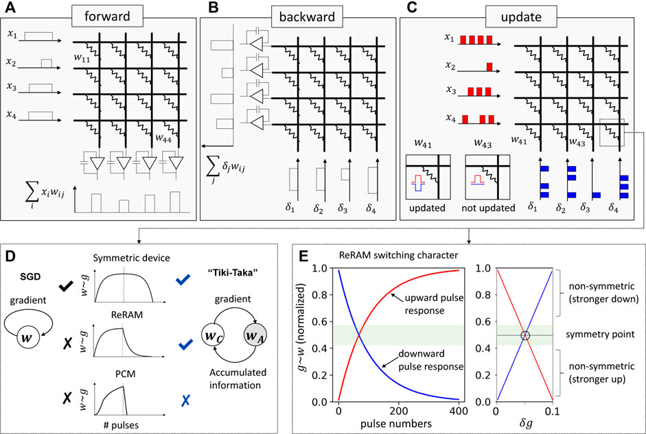
FIGURE 1. Schematics for RPU array describing (A) forward pass, (B) backward pass, and (C) update pass. The update procedure utilizes the stochastic gradient descent algorithm where the randomized pulse sequences are sent to rows and columns. Those cells where the pulses coincide get updated (e.g., w41). Otherwise, the cell is not updated (e.g., w43) (Haensch et al., 2019). (D) Schematics of ideal device characters, which have a bidirectional switching response and are symmetric to the negative/positive switching pulses. Such a character is suitable for SGD algorithm. However, the realistic device character is different. ReRAM shows a bidirectional but nonsymmetric switching character, and PCM exhibits unidirectional with a highly nonsymmetric switching character. Those are not suitable for the SGD algorithm, but the modified SGD (Tiki-Taka) algorithm can accommodate ReRAM-like switching characters (Gokmen and Haensch, 2020). (E) Typical ReRAM conductance response to the multiple voltage pulses. The red line depicts the response to the upward pulse, and blue line describes the response to the downward pulse. The differential conductance shown on the right panel of (E) describes the symmetry point where the conductance changes to the upward/downward response are equal.
2 Parallelized weight update in resistive memory and its challenges
The weight update in most of the NN algorithms relies on stochastic gradient descent (SGD) algorithm (Bottou, 1991). The SGD algorithm follows the update rule:
where wij is a logical weight representation at the ith row and jth column, x = [x1, …, xi, … ] is the input/activation vector propagated during the forward pass, δ = [δ1, …, δj, … ] is the error vector computed during the backward pass, and η is a hyperparameter controlling the strength of the update. Each of the logical weights is encoded as a conductance of an NVM device in RPU as
where K is an arbitrary scaling factor to map physical conductance to the logical weight representation, gij is a physical device conductance, and gij,ref is a reference conductance. Since weights are signed values and conductance is always positive, a differential signal is created by comparing the changing conductance gij,ref to a reference value.
A parallel operation of the outer product in Eq. 1 is a pivotal operation to accelerate the training procedure in RPU, and it is achieved by using the stochastic pulsing scheme, namely, xi and δj are encoded in time as a pulse train (Gokmen and Vlasov, 2016). Figure 1C illustrates the corresponding pulse train and the device at the cross-point where a row pulse and a column pulse coincide sees the full bias and is updated. The pulse train consists of a fixed bias and constant length pulses whose specific values are determined by details of the device characteristics. The stochastic pulsing scheme relies on a simple statistics of the coinciding events of row and column pulses. This means that the time-encoded pulse trains of x and δ can be sent for all the relevant rows and columns at once and the corresponding weight matrix w can be updated at a constant time. However, a caveat is that performing the weight update in parallel is achieved at an expense of the ability to check the status of the weights. In other words, we are no longer able to rely on a write-and-verify method for an update operation. This puts strict requirements on the switching characteristics of the cross-point elements for a successful SGD algorithm (Gokmen and Vlasov, 2016), which seems to be unfeasible with currently available non-volatile memory technology. A number of device non-idealities, including non-linearity in update and variations of device characteristics, have been discussed, and a symmetrical bidirectional write capability has been identified as one of the most important requirements (Gokmen and Vlasov, 2016). The first plot of Figure 1D illustrates the symmetrical bidirectional writing which requires the same amount of increase/decrease of the conductance in the resistive elements for applied stochastic pulses. However, the realistic devices show switching characteristics far from the ideal. For example, the phase change memory (PCM) exhibits unidirectional switching behavior with highly nonsymmetric set/reset characteristics. The resistive random-access memory (ReRAM) exhibits bidirectional switching yet shows a highly nonsymmetric update character (Haensch et al., 2019). Figure 1E describes a typical ReRAM conductance (g) pulse response. The device shows large changes for downward pulses when g is close to its maximum, whereas small incremental changes for the upward pulses in the same region. Such a nonsymmetric conductance change, δg, is described in the right side panel of Figure 1E for the entire conductance range and clearly illustrates that conductance change is not equal for upward (red)/downward (blue) update pulses.
Interestingly, there is a point, which we call as a symmetry point (SP), where the device responses to upward/downward pulses are identical. The SP can be also defined as a specific conductance that reaches from arbitrary initial conductance when the device is stimulated by a random number of equally distributed upward/downward pulses (Kim et al., 2019a) (see Supplementary Figure S2). When the device is operating near the SP, the response to the upward/downward update pulse is nearly symmetric, and thus the device may behave for SGD algorithm. During the operation, however, the conductance will not necessarily converge to the SP, rather its stationary value will be determined by the competing requirements of reaching a minimum of the network’s loss function. Let us assume that there is a target weight at which an ideal symmetric device converges, wt, which corresponds to a local minimum of the defined loss function. When the device is operating far from SP, a stronger update on one side tends to force the device fluctuating below/above wt, thus hindering the device from learning the correct algorithmic weight value, wt. A more detailed illustration is given in Supplementary Figures S1A–C. Improvement in materials and optimizing device stack has been made for better update characters; however, challenges remain such as having limited resistance range (Prezioso et al., 2015) or process maturity (Kim et al., 2019b). Optimizing pulse sequence (Chen et al., 2015) or an analog/digital hybrid system (Le Gallo et al., 2018) may mitigate the non-idealities of the device; however, they come with a cost of severe reduction in the training speed.
3 Algorithm optimization for improved parallel update
The recent advances in training algorithms relax the criteria for a device asymmetry (Gokmen and Haensch, 2020; Onen et al., 2022) with a modified SGD algorithm, or Tiki-Taka algorithm. The key advance is made by separating a gradient processing and an error backpropagation into two coupled systems, A (WA) and C (WC), respectively. Figure 2 describes the difference between (a) the conventional SGD and (b) the Tiki-Taka algorithm. Specifically, the modified update rule follows
where λ is the learning rate for system C and wA,C is the weight representation of the systems A and C, respectively. The important caveat is to utilize SP as gij,ref for system A. The conductance of the reference device for wC does not need to be at the SP of its active device, as we shall see in the following paragraphs. The forward pass utilizes wC to compute gradients, and the gradients are separately processed by wA. Then, the processed gradients are transferred to wC with a pre-defined rate (e.g., every nth training data). When the desirable weight is not reached for wC, a biased gradient is accumulated on wA which eventually drives wC toward the desired local minima upon the scheduled transfer. Once the desirable weight is reached for wC, the stimulus for system A ideally becomes zero as there is no systematic information generated by the gradient processing performed by the system A. However, due to the device noise and non-idealities, a random signal with (close to) equal upward/downward updates are generated and accumulated in system A. This randomly distributed upward/downward signal will drive the active conductance in wA to the SP. It should be noted that we intentionally put gij,ref of system A to SP, thus the resulting signal from A is ideally zero. Of course, due to the device noise and non-ideality, system A may fluctuate near zero, but more importantly, such fluctuation is less likely to cause any significant deviation of system C from its local minima as system A now operates near SP. Consequently, the resulting weight of system A will be nearly zero, and henceforth there will be no significant net update for wC as well. This guarantees that the weights in wC will reach the algorithmically determined target (see Supplementary Figures S1E,F) for further illustration of an example where the system reaches the desirable value through the feedback process between wA and wC.
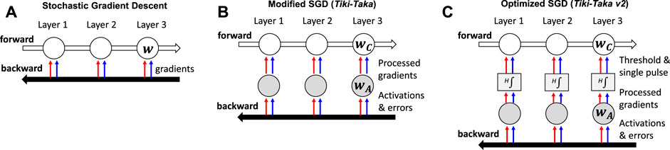
FIGURE 2. (A) Schematics for conventional SGD algorithm. (B) Schematics for Tiki-Taka algorithm. (C) Schematics for further improved Tiki-Taka v2 algorithm.
Tiki-Taka brings additional hardware complexity compared to SGD. System A can be realized using two devices, where one is used as a reference device that is programmed to the symmetry point of the updated device. In addition, system C requires one more additional device to encode the logical C value. It should be noted that the same reference device used for A can be used for C because the symmetry point shifting is not required for system C. As a result, Tiki-Taka requires three device arrays compared to the two needed for SGD. However, one additional device array required by Tiki-Taka is readily justifiable as Tiki-Taka significantly reduces the critical device requirements that the technology must deliver for successful training.
The benefit of having the coupled systems A and C is to alleviate the requirement on the device symmetry by enabling system A to operate near SP, thus providing a better convergence toward minimizing the defined loss function. However, the noise introduced during the transfer from system A to C often causes an additional test error (Gokmen, 2021). The fluctuation can be further mitigated by introducing an additional stage, H, as illustrated in Figure 2C. Here, H is introduced between A and C and wA is accumulated in H at a given rate. The H stage performs the integration in a digital domain and outputs a single-pulse update to wC when the integrated value is above a certain threshold hth. The integration and thresholding act as a low-pass filter, and the model parameter is updated at a slower rate with higher confidence. This enables the algorithm to cope with various hardware-related noise issues. The modified update rule is
where wC,ij is the ith row and jth column element of wC and δwmin is the minimum update unit (e.g., corresponds to a conductance change by a single-update pulse).
This improved version of the Tiki-Taka algorithm, referred to as Tiki-Taka v2 (Gokmen and Haensch, 2020), requires more hardware footprint to accommodate additional digital storage of H. However, these additional costs are justifiable, as it also brings additional robustness against key hardware issues (noise and the limited number of states) while only causing modest performance degradation (Gokmen and Haensch, 2020).
4 Device demonstration
4.1 Discrete device demonstration, one-variable task
We perform a one-variable learning task to show the feasibility of the Tiki-Taka algorithm. We choose a target slope value (equivalent to the target weight value, wt) and learn the slope by using either SGD or Tiki-Taka algorithm. The training dataset is generated from randomly sampled x values that satisfy X0 ∈ [ − 1, 1] and the corresponding y values that satisfy Y0 = wtX0 with a small Gaussian noise. Then, the training input X0 is fed into the network, and the L2 norm is calculated from the fitting result Y and the desirable output Y0. The procedure is summarized as a flow chart in Figure 3A, and an example outcome is described in Figure 3B.
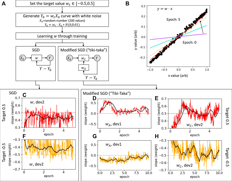
FIGURE 3. (A) Flow chart of a linear regression task. (B) Example plot describes the procedure explained in (A). Black circle symbols are training datasets (X0, Y0). Solid line shows the learned weight from 0 to 5 epochs. During the training, the resultant conductance value has been converted to a logical weight value by normalizing the conductance to the minimum (gmin) and maximum (gmax) values of each device, or w = (g − gSP)/(gmax − gmin + δ), where δ is an arbitrary buffer value that ensures we address a weight range of [ − 0.5, 0.5]. (C–H) Weight evolutions for SGD and “Tiki-Taka” algorithm. (C) Device 2 in Supplementary Figure S2 is utilized for SGD algorithm to learn wt = 0.5 (dashed line). The solid red line shows the weight evolution as a function of epoch. The black thick solid line represents the moving average of the weight evolution with the average window of 0.5 epoch. Due to the nonsymmetric update nature of the device, w fluctuates below wt. (D,E) wA and wC evolution for “Tiki-Taka” algorithm. Initially, the upward gradient is accumulated in wA, leading to a monotonic increase in wC. Once wC reaches wt, wA fluctuates near the SP (or wA = 0). wA remains slightly higher than 0 and drives wC to fluctuate near the target unlike SGD in (C). The same corresponding experiment is presented for wt = −0.5 in (F) and (G,H).
We utilize the two 20μm × 20 μm ReRAM devices. The devices are prepared with a TiN/HfOx (5 nm)/TiN stack and individually wired out to the external pads. The device is formed and goes through multiple switching cycles to confirm the reproducible switching characteristics. The detailed device pulse response and conditions are described in Supplementary Appendix S7. Figure 3C shows the SGD approach to learn the slope value of wt = 0.5, which is close to the maximum conductance value. In this case, device 2 is operating far from the SP, and the updates are nonsymmetric. The weight clearly fluctuates below wt for the reasons discussed in Section 2. Once we adopt the Tiki-Taka algorithm, wA accumulates the gradients and fluctuates near the SP (zero in weight). It should be noted that in Figure 3E, wA shows that its averaged weight remains slightly above 0. This is due to the nonsymmetric update nature of the device, namely, from more upward update requests accumulated to wA. This positive wA drives wC toward a higher value than that in SGD algorithm until it reaches the desirable value wt (see Section 3 for more analysis). Figure 3F shows that wC now reaches the target value of wt = 0.5 and fluctuates around it. When the target slope is set close to the minimum conductance value of wt = −0.5, Figures 3D–F show a similar trend. This result shows that the nonsymmetric device can now be applied to NN learning.
4.2 2 × 2 array demonstration, two-variable task
After our trial on individual devices, we scale our problem for a 2 × 2 array. The main motivation is to test out the feasibility of the algorithm in a more realistic 1T1R ReRAM array environment. The same linear regression task is considered as described in Figure 3A, but now we fit for both the slope and y-intercept. Figure 4A shows the ReRAM stack in the 1T1R array. Four 200nm × 200 nm devices out of a 32 by 20 array are selected. We found a common switching condition of − 2.1V/2.0V with 1.6μs pulses. The gate is controlled row-wise, and thus the half-bias is applied to the unselected rows and columns. This allows us to implement the stochastic pulse scheme described in Figure 1C, while minimizing the disturbance of unselected rows and columns. A clear response has been observed for a selected device, whereas the devices in disturbance show no evidence of systematic drift of the conductance state. For more details, see Supplementary Appendix S8. Knowing the minimal disturbance impact, we apply SGD and Tiki-Taka for the linear regression task. To accommodate for the device variations, we choose the bias conditions showing reasonable responses for four devices. Therefore, the pulse may not be ideally optimized for individual devices, indicating higher fluctuations in weight values in Figure 4C. In addition, the fluctuation in both the slope and y-intercept results in the fitting results being worse, indicated as gray individual lines in Figure 4C. SGD results in an average learned slope and y-intercept which is not exactly satisfying the desirable value due to the nonsymmetric nature of the device response. In addition, the high level of conductance fluctuation shows that the multi-variable fitting is not feasible. To address the high noise, we utilize the further modified SGD or Tiki-Taka v2 algorithm (Gokmen, 2021) which is effective in mitigating various hardware noises as discussed in Section 3 and Figure 2C. The fitting results shown in Figure 4F are now more stable in terms of tolerating noise. The averaged weight value reaches the desirable target values, overcoming the nonsymmetric device nature. Figure 4F illustrates the dramatic improvement in training by carefully optimizing the learning algorithm.
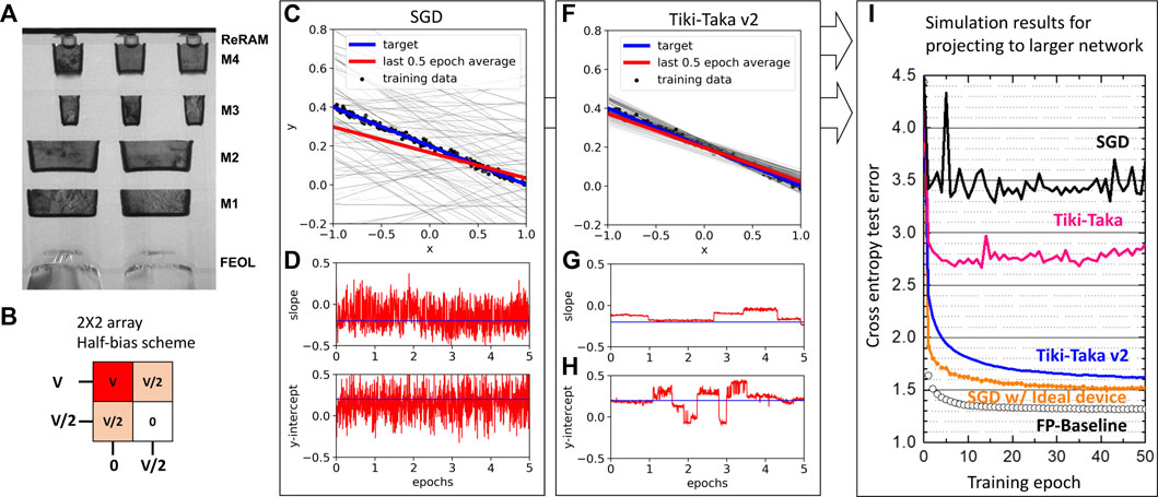
FIGURE 4. 2 × 2 array pulse/disturbance response. (A) Cross-sectional TEM image of 1T1R devices. (B) Row and column bias scheme for the half-selection scheme. The gate is applied to the first row. The full bias is applied to the (1,1) device, and the half-bias is applied to (2,1) and (1,2) devices. (C–H) Two-variable fitting results using the 2 × 2 array. The target slope (−0.25) and y-intercept (−0.25) are learned through (C) SGD algorithm, and the weight evolutions are depicted for the (D) slope and (E) y-intercept. (F) Same task is performed using the optimized “Tiki-Taka” algorithm. Corresponding wC values are plotted for the (G) slope and (H) y-intercept. (I) Simulation results using doubly stacked LSTM network trained on Leo Tolstoy’s War and Peace (WP) novel. Open circles are the cross entropy test error of the training results with the floating point (FP). Orange closed circles are SGD using the ideal (symmetric update, 1200 states, baseline 1x noise) device. Simulation results using baseline ReRAM stack characters (nonsymmetric update, 15 states, 260x noise). Simulation results using improved ReRAM stack characters (nonsymmetric update, 50 states, 96x noise). We observe the test error close to the FP using SGD for ideal symmetric device characteristics (rectangular symbols). However, the network exhibits the degradation of the test error when we introduce the nonsymmetric typical ReRAM characteristics (black lines). The improvement is observed by utilizing the “Tiki-Taka” training algorithm (Gokmen and Haensch, 2020) (magenta lines) and further improved by using the optimized “Tiki-Taka” algorithm (Gokmen, 2021) (blue lines).
5 Conclusion
We utilize our baseline device and project the model accuracy of the long short-term memory (LSTM) network through simulation. The details of the LSTM network and dataset are described in Gokmen and Haensch (2020). Figure 4I illustrates a significant reduction in the test error by adopting Tiki-Taka v2 algorithm. The practical implementation of the algorithm in a large-scale array still requires improvements in device characteristics and variabilities, especially having a common operation conductance range and switching bias conditions is of importance for larger scale demonstration of this algorithm. It is important to note, however, that the modified and optimized algorithm not only relaxes a requirement for symmetric update but also increases noise robustness and reduces the required number of states significantly. We demonstrate that the goal of realizing the NN training accelerator maybe within the reach by further co-optimizing the learning algorithm and device.
Data availability statement
The raw data supporting the conclusion of this article will be made available by the authors, without undue reservation.
Author contributions
YK, JD, and RK carried out measurements. YK, TG, and TA analyzed the results. SK and PS designed/configured the experimental setup. HM and AR fabricated the device. TG performed numerical simulation. YK, TG, VN, and TA wrote the manuscript.
Acknowledgments
The authors thank the staff and management of IBM Microelectronics Research Lab for their contributions to the device fabrication. This work was supported by the IBM Research AI Hardware Center (ibm.co/ai-hardware-center).
Conflict of interest
Authors YK, TG, HM, PS, SK, AR, JD, RK, VN, and TA were employed by IBM Thomas J. Watson Research Center.
Publisher’s note
All claims expressed in this article are solely those of the authors and do not necessarily represent those of their affiliated organizations, or those of the publisher, the editors, and the reviewers. Any product that may be evaluated in this article, or claim that may be made by its manufacturer, is not guaranteed or endorsed by the publisher.
Supplementary material
The Supplementary Material for this article can be found online at: https://www.frontiersin.org/articles/10.3389/fnano.2022.1008266/full#supplementary-material
Supplementary Figure S1 | Schematics for (A–C) SGD and (D–F) “Tiki-Taka” algorithm.
Supplementary Figure S2 | (A) 20 μm × 20 μm ReRAM (device 1) conductance response to the 400 upward/400 downward pulses. The measurement is repeated for five cycles (gray-filled circle), and averaged traces are plotted as a solid line. Repeated two upward/two downward pulse sequence has been used to measure the symmetry point (SP, open circle). The SP is obtained by averaging measured conductance from half of the sequence up to the final sequence (dashed line). (B) Differential conductance is obtained from averaged traces from (A). SP agrees with the point where the differential conductance of up/down traces matches with each other. SP is indicated as a dashed line with its rms as a shaded region. We observe that the SP extracted from upward/downward traces does not exactly match with the SP extracted from alternating pulse measurement results, which is caused by the inherent device noise and cycle-to-cycle variation. (C) Same measurement with (A) for another device (device 2). (D) Corresponding differential conductance measurement. The devices have been formed at 3 V. The 320-ns pulse is used for −1.48 V (down)/1.28 V (up) for device 1 and −1.7 V (down)/1.15 V (up) for device 2. We use device 1 as WA and device 2 as WC.
Supplementary Figure S3 | (A) (row,column) = (1,1) device is selected, and full bias response for the upward/downward pulse is clearly observed. (1,2) and (2,1) devices are half-selected, respectively. A random fluctuation has been observed. The (2,2) device is unselected, and no fluctuation has been observed. (B) Similar experiment is carried out but by selecting the (2,1) device. The device has been tested under five super cycles of upward/downward pulse sequences, and the response is indicated as gray symbols. The averaged upward/downward pulse responses are indicated as blue/red solid lines, respectively.
References
Agrawal, A., Choi, J., Gopalakrishnan, K., Gupta, S., Nair, R., Oh, J., et al. (2016). Rebooting computing and low-power image recognition challenge, in 2016 IEEE International Conference on Rebooting Computing (ICRC) 17-19 October 2016, San Diego.
Bottou, L. (1991). “Stochastic gradient learning in neural networks,” in Proc. Neuro-Nımes. Nimes, France: EC2. Available at: http://leon.bottou.org/papers/bottou-91c.
Chen, P.-Y., Lin, B., Wang, I.-T., Hou, T.-H., Ye, J., Vrudhula, S., et al. (2015). IEEE, 194–199.Digest of technical papers2015 IEEE/ACM International Conference on Computer-Aided Design (ICCAD)02-06 November 2015Austin
Chen, Y.-H., Krishna, T., Emer, J. S., and Sze, V. (2017). Eyeriss: An energy-efficient reconfigurable accelerator for deep convolutional neural networks. IEEE J. Solid-State Circuits 52, 127–138. doi:10.1109/jssc.2016.2616357
Choi, J., Venkataramani, S., Srinivasan, V. V., Gopalakrishnan, K., Wang, Z., and Chuang, P. (2019). in Proceedings of machine learning and systems. Editors A. Talwalkar, V. Smith, and M. Zaharia (Morehouse: Curran Associates, Inc.).
Collobert, R., Weston, J., Bottou, L., Karlen, M., Kavukcuoglu, K., and Kuksa, P. (2011). Natural language processing (Almost) from scratch. J. Mach. Learn. Res. 12, 2493–2537. doi:10.5555/1953048.2078186
Gokmen, T. (2021). Enabling training of neural networks on noisy hardware. Front. Artif. Intell. 4, 699148. doi:10.3389/frai.2021.699148
Gokmen, T., and Haensch, W. (2020). Algorithm for training neural networks on resistive device arrays. Front. Neurosci. 14, 103. doi:10.3389/fnins.2020.00103
Gokmen, T., and Vlasov, Y. (2016). Acceleration of deep neural network training with resistive cross-point devices: Design considerations. Front. Neurosci. 10, 333. doi:10.3389/fnins.2016.00333
Haensch, W., Gokmen, T., and Puri, R. (2019). The next generation of deep learning hardware: Analog computing. Proc. IEEE 107, 108–122. doi:10.1109/jproc.2018.2871057
Hinton, G., Deng, L., Yu, D., Dahl, G. E., Mohamed, A.-r., Jaitly, N., et al. (2012). Deep neural networks for acoustic modeling in speech recognition: The shared views of four research groups. IEEE Signal Process. Mag. 29, 82–97. doi:10.1109/msp.2012.2205597
Ielmini, D., and Wong, H.-S. P. (2018). In-memory computing with resistive switching devices. Nat. Electron. 1, 333–343. doi:10.1038/s41928-018-0092-2
Jones, N. (2018). How to stop data centres from gobbling up the world’s electricity. Nature 561, 163–166. doi:10.1038/d41586-018-06610-y
Jouppi, N. P., Young, C., Patil, N., Patterson, D., Agrawal, G., Bajwa, R., et al. (2017). In-datacenter performance analysis of a tensor processing unit. SIGARCH Comput. Archit. News 45, 1–12. doi:10.1145/3140659.3080246
Kim, H., Rasch, M., Gokmen, T., Ando, T., Miyazoe, H., Kim, J.-J., et al. (2019). Zero-shifting technique for deep neural network training on resistive cross-point arrays. arXiv:1907.10228 [cs.ET].
Kim, S., Todorov, T., Onen, M., Gokmen, T., Bishop, D., Solomon, P., et al. (2019). IEDM 2019 welcome, in 2019 IEEE International Electron Devices Meeting (IEDM) 07-11 December 2019, San Francisco.
Krizhevsky, A., Sutskever, I., and Hinton, G. E. (2012). in Advances in neural information processing systems. Editors F. Pereira, C. Burges, L. Bottou, and K. Weinberger (Morehouse: Curran Associates, Inc.).
Le Gallo, M., Sebastian, A., Mathis, R., Manica, M., Giefers, H., Tuma, T., et al. (2018). Mixed-precision in-memory computing. Nat. Electron. 1, 246–253. doi:10.1038/s41928-018-0054-8
LeCun, Y., Bengio, Y., and Hinton, G. (2015). Deep learning. nature 521, 436–444. doi:10.1038/nature14539
Onen, M., Gokmen, T., Todorov, T. K., Nowicki, T., del Alamo, J. A., Rozen, J., et al. (2022). Neural network training with asymmetric crosspoint elements. Front. Artif. Intell. 5, 891624. doi:10.3389/frai.2022.891624
Keywords: analog computing, resistive RAM, neural network acceleration, cross-bar array architecture, neural network training, in-memory computing
Citation: Kim Y, Gokmen T, Miyazoe H, Solomon P, Kim S, Ray A, Doevenspeck J, Khan RS, Narayanan V and Ando T (2022) Neural network learning using non-ideal resistive memory devices. Front. Nanotechnol. 4:1008266. doi: 10.3389/fnano.2022.1008266
Received: 31 July 2022; Accepted: 10 October 2022;
Published: 31 October 2022.
Edited by:
Pavan Nukala, Indian Institute of Science (IISc), IndiaReviewed by:
Harshit Agarwal, Indian Institute of Technology Jodhpur, IndiaZongwei Wang, Peking University, China
Copyright © 2022 Kim, Gokmen, Miyazoe, Solomon, Kim, Ray, Doevenspeck, Khan, Narayanan and Ando. This is an open-access article distributed under the terms of the Creative Commons Attribution License (CC BY). The use, distribution or reproduction in other forums is permitted, provided the original author(s) and the copyright owner(s) are credited and that the original publication in this journal is cited, in accordance with accepted academic practice. No use, distribution or reproduction is permitted which does not comply with these terms.
*Correspondence: Youngseok Kim, eW91bmdzZW9rLmtpbTFAaWJtLmNvbQ==