- 1Department of Electrical and Computer Engineering, The University of Texas at Austin, Austin, TX, United States
- 2Intel Corporation, Hillsboro, OR, United States
- 3Oracle Corporation, Austin, TX, United States
Resistive random-access memory (RRAM) devices have drawn increasing interest for the simplicity of its structure, low power consumption and applicability to neuromorphic computing. By combining analog computing and data storage at the device level, neuromorphic computing system has the potential to meet the demand of computing power in applications such as artificial intelligence (AI), machine learning (ML) and Internet of Things (IoT). Monolayer rhenium diselenide (ReSe2), as a two-dimensional (2D) material, has been reported to exhibit non-volatile resistive switching (NVRS) behavior in RRAM devices with sub-nanometer active layer thickness. In this paper, we demonstrate stable multiple-step RESET in ReSe2 RRAM devices by applying different levels of DC electrical bias. Pulse measurement has been conducted to study the neuromorphic characteristics. Under different height of stimuli, the ReSe2 RRAM devices have been found to switch to different resistance states, which shows the potentiation of synaptic applications. Long-term potentiation (LTP) and depression (LTD) have been demonstrated with the gradual resistance switching behaviors observed in long-term plasticity programming. A Verilog-A model is proposed based on the multiple-step resistive switching behavior. By implementing the LTP/LTD parameters, an artificial neural network (ANN) is constructed for the demonstration of handwriting classification using Modified National Institute of Standards and Technology (MNIST) dataset.
Introduction
With the rapid development of artificial intelligence (AI), machine learning (ML) and Internet of Things (IoT), novel computing technology for information processing is becoming crucial (Moh and Raju, 2018; Mohanta et al., 2020; Zhu et al., 2020). Conventional circuits based on von Neumann architecture are facing challenges including physical separation of computing units and memory, and low density of on-chip memories, which in turn lead to high energy consumption and low operation efficiency (Du Nguyen et al., 2017; Zidan et al., 2018; Amirsoleimani et al., 2020; Sebastian et al., 2020). Therefore, neuromorphic computing, which is inspired by the operation of human brains, has been proposed as a promising computing paradigm to overcome the bottleneck of von Neumann architecture (Kuzum et al., 2013). To physically realize the design of neuromorphic computing circuits, development of novel devices that can directly mimic brain-like long-term potentiation and depression (LTP/LTD) behaviors therefore arise significant interest.
Resistive random-access memory (RRAM), also known as memristors, is one of the most competitive candidates for the application of neuromorphic computing (Hong X. et al., 2018). The operation of RRAM devices is based on the non-volatile resistive switching (NVRS) phenomenon of the active layer, typically a bulk metal-oxide film, such as SiO2 or HfO2, in a metal-insulator-metal (MIM) stacking structure (Chang et al., 2016; Lin et al., 2017). By applying external electrical bias, repeatable resistive switching behavior between high resistance state (HRS) and low resistance state (LRS) can be observed in the device and can be subsequently sustained without power supply (Wong et al., 2012). In recent years, two-dimensional (2D) materials have been investigated and applied in the development of the next generation nanoelectronics, optoelectronics, flexible electronics, and biosensors. Various 2D materials, including graphene oxide, solution-processed transitional metal dichalcogenides (TMDs), degraded black phosphorus and multilayer hexagonal boron nitride (h-BN), have been reported to exhibit NVRS phenomenon and applied in RRAM devices (Bai et al., 2015; Han et al., 2017; Ge et al., 2018; Wu et al., 2019). It has been reported in our previous work that monolayer chemical vapor deposition (CVD)-grown rhenium diselenide (ReSe2) shows intrinsic NVRS phenomenon in a vertical MIM configuration (Wu et al., 2021). The structure holds promise for practical integration with smaller die space and 3D stacking capability.
Analog resistive switching has been realized in metal-oxide-based as well as 2D-material-based RRAM devices in the early work (Shen et al., 2020; Cao et al., 2021). Compared with the conventional binary switching with only two stable resistance states, RRAM devices with analog switching property can potentially mimic the function of biological synapse, making them feasible to be implemented in brain-inspired neuromorphic computing systems (Li et al., 2017; Zhang et al., 2019; Wang et al., 2021). When designing circuits with RRAM devices, Verilog-A provides a good platform for compact analog modeling as a de facto standard language widely used in semiconductor industry (Jiang et al., 2014; Mcandrew et al., 2015). By fitting the experimental data into functions of resistance and voltage, resistive switching behaviors can be described by a well-designed Verilog-A model.
In this work, RRAM devices in vertical MIM structure based on monolayer ReSe2 were fabricated. Raman and photoluminescence (PL) spectra have been conducted to characterize the 2D material used in the devices. DC and pulse measurements are used to demonstrate the electrical properties of the ReSe2 RRAM devices including resistive switching, retention, endurance, and LTP/LTD behaviors. A Verilog-A model has been established based on the experimental data. To study the interference to a neuromorphic computing system brought by the ReSe2 RRAM device, an artificial neural network (ANN) is simulated for pattern recognition using Modified National Institute of Standards and Technology (MNIST) dataset.
Experiments
Device Fabrication
The monolayer CVD-grown ReSe2 films on mica substrate were produced by Sixcarbon Technology. All the fabricated devices in this work make use of the crossbar MIM structure. The 2D RRAM devices are fabricated with continuous CVD-grown monolayer ReSe2 film sandwiched between Au top and bottom electrodes in the vertical MIM structure. The active device area is defined as the overlapped region between the crossbar electrodes. Figures 1A,B show the schematic and top-view optical image of the ReSe2 RRAM devices, respectively. The active layer thickness is below 1 nm for the monolayer ReSe2. Gold, which is an inert metal, is used as the electrode material in this work to avoid the possible formation of metal oxides at the metal-ReSe2 interface.
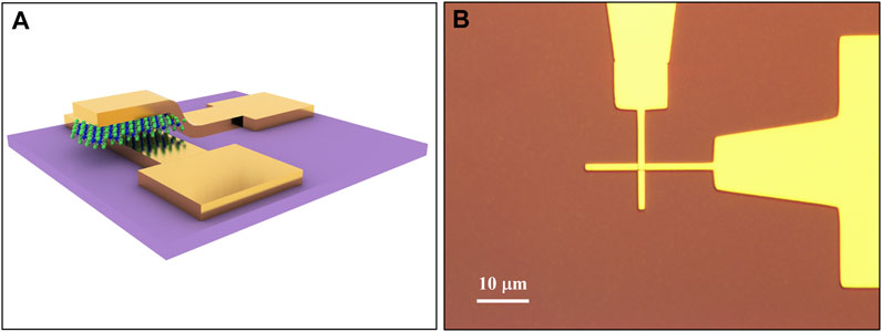
FIGURE 1. RRAM device based on monolayer ReSe2. (A) 3D schematic and (B) optical image of fabricated ReSe2 vertical MIM crossbar device with Au electrodes.
The bottom electrodes (BE) were patterned by e-beam lithography and deposited by e-beam evaporation (2 nm Cr/ 80 nm Au) on a 285 nm SiO2/Si substrate. Polydimethylsiloxane (PDMS) pick-and-place water assisted transfer method was used to transfer the monolayer ReSe2 film from mica to the target substrate with BE (Ma et al., 2017). In this method, the ReSe2 film contacts with the PDMS stamp conformally. Then, the mica-ReSe2-PDMS system was soaked into deionized water for 30 min. During this process, water can diffuse into the interface between ReSe2 and mica due to the hydrophilic surface of mica. The ReSe2-PDMS film was separated from the mica substrate and brought into contact with the target substrate. The PDMS stamp was peeled off subsequently and the ReSe2 film was left on the target substrate with BE. After the completion of transfer, top electrodes (TE) were patterned and deposited with the same method as BE. The overlapped region between TE and BE is defined as the device area with a typical size of 1 × 1 and 2 × 2 μm2 in this work.
Material and Electrical Characterization
Raman spectroscopy and photoluminescence (PL) were performed on a Renishaw in-Via system with 532 nm wavelength source to evaluate the ReSe2 film before transferring. The DC and pulse characteristics of the devices were taken on a Cascade probe station under ambient conditions. An Agilent B1500A semiconductor parameter analyzer was used for DC and pulse measurements. During the DC measurements, electrical bias was applied on TE and BE was grounded. By involving one additional probe for pulses on TE, voltage pulses were injected to the device for pulse measurements.
Verilog-A Model
To describe the analog switching behavior of ReSe2 RRAM devices, a compact Verilog-A model was constructed based on the data from DC and pulse measurements. By fitting the analog switching data into functions of resistance and voltage, the model was then used to simulate analog resistive switching and LTP/LTD behaviors when implemented in HSPICE.
Artificial Neural Network Simulation
A fully connected multi-layer perceptron ANN model was designed for supervised learning with the MNIST database. To demonstrate the potential application of the ReSe2 RRAM devices, LTP/LTD characteristics were implemented in the stochastic gradient descent (SGD) optimizer of the ANN model.
Results and Discussions
Material characterizations have been conducted on the samples to confirm the material used in the device. Raman spectra of the monolayer ReSe2 films (Figure 2A) has been used to confirm the quality of material. The two characteristic peaks for ReSe2, were observed at ∼190 cm−1 and ∼140 cm−1, corresponding to the Ag-like mode and Eg-like mode of 2H ReSe2. The peak distance of ∼50 cm−1 is in a good agreement with the reported value, suggesting a high-qualify uniform monolayer crystalline film (Jiang et al., 2018; Apte et al., 2019). Figure 2B shows the PL of the monolayer ReSe2. The PL peak position for the ReSe2 is located at ∼1.5 eV, consistent with the reported optical band gap (Hong M. et al., 2018; Qiu et al., 2019).
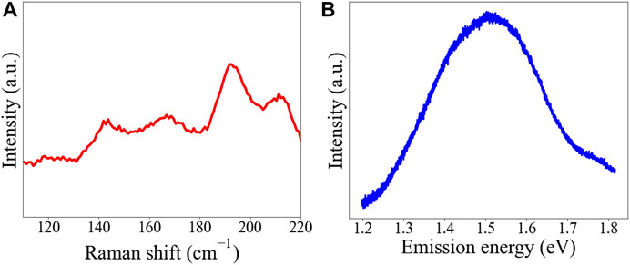
FIGURE 2. Material characterization of monolayer ReSe2. (A) Raman shift spectra and (B) photoluminescence.
DC electrical measurements were performed on as-fabricated crossbar MIM RRAM devices and revealed nonvolatile resistive switching in monolayer ReSe2 active layers. Figure 3A shows a typical I-V curve of resistive switching. The device generally starts from a HRS. Without any forming process, the current shows a sudden increase as voltage sweeps to ∼3 V, indicating a transition from HRS to LRS (SET). For bipolar operation, the device will start a multi-step analog transition to HRS from −0.5 V (RESET) when a reverse voltage sweep is applied, which shows the potential for neuromorphic applications. A compliance current of 1 mA is applied at SET process to prevent irreversible breakdown, while no compliance current is applied at RESET process. The grey curves in Figure 1A illustrates a low cycle-to-cycle variation. After each SET and RESET measurement process, a read process is applied to acquire the resistance of the device. The LRS of the device is around 50 Ω, while the HRS can reach up to over 1 × 10⁶ Ω, highlighting a promising ON/OFF ratio of over 4 orders of magnitude. Manual endurance data shown in Figure 3B demonstrates over 200 DC cycles, which is similar to the endurance data of metal oxide-based RRAM devices. Retention of nonvolatile states tested up to 6 h (Figure 3C) without obvious resistance change, which is sufficient for certain neuromorphic applications involving short term plasticity.

FIGURE 3. Electrical characteristics of ReSe2 RRAM devices. (A) I-V characteristic under cycling DC sweep, indicating low cycle-to-cycle variation. (B) Endurance of ReSe2 RRAM devices for over 200 cycles. (C) The retention behavior of ReSe2 RRAM devices for over 6 h at ambient condition.
Based on our previous studies on 2D TMD-based RRAM devices, a “conductive-point” model was proposed to illustrate the resistive switching mechanism (Wu et al., 2020; Wu et al., 2021). When applying external voltage bias, metal ions/atoms from TE can be dissociated triggered by the electrical field and adsorbed into the chalcogen defects in the ReSe2 layer. As electrons transport through the metallic conductive point at the vacancy site, the device would go into a lower resistance state. During the RESET process, the Joule heating effect induced by the high current in the device would move the metal ions/atoms out of the vacancies, resulting in a transition to a higher resistance state. Atomic resolution STM measurement with the evidence of Au moving in and out from the vacancy site after SET and RESET process supports the model. Figure 4 shows the schematics of the conductive-point model with metal adsorption.
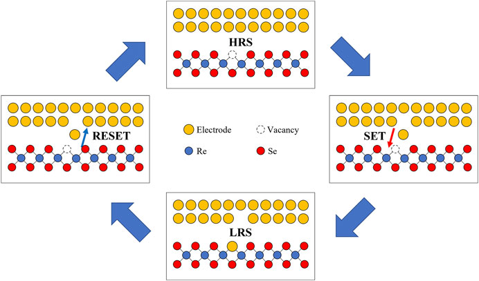
FIGURE 4. Schematics of the conductive-point model with metal adsorption. Starting from HRS, Au ions or atoms from the electrodes will be driven by external voltage bias and diffuse to Se vacancies in the active layer (SET), leading the device to LRS. While applying RESET voltage, the Au ions or atoms will be moved out of the vacancies by current-induced Joule heating effect, resulting in a transition to a higher resistance state.
After the DC characterization, variable pulses are applied to the ReSe2 devices to access its capability of emulating LTP and LTD. In this work, the selected pulse setup for SET is 100 ns in width and 3.2 V in height after a series of tuning. While for RESET, the pulse setup is 100 ns in width and −0.8 V in height. A DC read process was applied after each pulse to acquire the resistance state. By applying the optimum SET/RESET pulses, the conductance of the ReSe2 device shows gradual increase/decrease. Figure 5 presents the LTP/LTD. The device exhibits a resistive transition from HRS to LRS after receiving 25 SET pulses (Figure 5A). While after 40 RESET pulses, the conductance gradually decreases from ∼2.4 mS to 1.8 mS (Figure 5B). Based on the conductive-point model, Au ions/atoms would be gradually driven into the active layer, leading to a multi-step conductance increase after a series of pulses. While in the pulse RESET process, the dissociation of Au ions/atoms from the active layer is relatively slower than DC RESET due to the low amount of power injected into the device by RESET pulses, resulting in a decrease of conductance after a larger number of pulses. In this way, we can mimic the synaptic responses of depression and potentiation by changing the polarization. As is shown in Table 1, among RRAM devices based on different types of low-dimensional materials including graphene oxide, hBN, metal dichalcogenides and quantum dots, ReSe2 RRAM demonstrated in this work is highlighted by its small pulse width, and relatively high ON/OFF ratio, which shows the potential in the large scale applications of neuromorphic computing system.
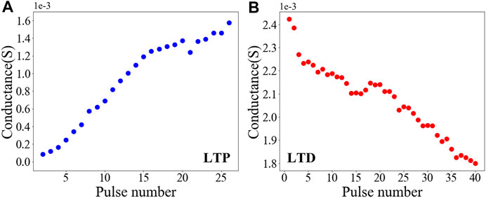
FIGURE 5. Demonstration of synapse behavior of the ReSe2 RRAM device. (A) Long-term potentiation (LTP) with 25 SET pulses. (B) Long term depression (LTD) with 40 RESET pulses.
With the acquisition of DC and pulse experimental data, a compact Verilog-A model is constructed. Based on the I-V characteristics from DC measurements, the LRS can be fitted with Ohmic conduction model, which illustrates the linear relation between voltage and current. For the analog RESET process, resistance states are fitted by Schottky emission model. This is consistent with our previous work. The following simplifications and functions are used in the construction of the Verilog-A model:
• The resistance states are continuous as the maximum voltage (
• The resistance of LRS is controlled by a metallic Ohmic conduction function as is shown in Function 1, where the parameter
• The resistance of HRS is derived from the Schottky emission model:
• The parameter
• The resistance of the RRAM device under LTP/LTD follows an exponential degradation function:
Here,
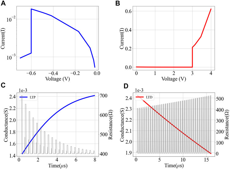
FIGURE 6. Simulation results of ReSe2 RRAM Verilog-A compact model using HSPICE. Simulated I-V curve of (A) RESET and (B) SET under DC sweep. No current compliance was applied to the simulation, causing an increasing current response after passing the threshold voltage of SET. Simulated (C) long-term potentiation, and (D) long term depression.
By implementing the LRS and HRS function fitted by data extracted from 20 resistive switching cycles, an analog Verilog-A compact model for the ReSe2 RRAM device is constructed. Figures 6A,B displays the HSPICE simulation result based on the Verilog-A model when applying DC sweep. The results obtained from the simulation indicate that the resistance switching occurs when the input voltage sweep across threshold voltage for SET and RESET, which are 3 V and −0.5 V, respectively. Further function implementation has been conducted based on the basic analog resistive switching model. The degradation rate fitted by function (4) enables the model to have LTP/LTD behavior when a series of pulse with the same height and width is input into the RRAM device in a HSPICE simulation. Figures 6C,D shows the simulated LTP/LTD results. The grey plots are the resistance output from the simulation. The blue and red curves are the calculated conductance states after each pulse, which shows similar behavior as the experimental results.
To demonstrate the potential of our synaptic ReSe2 RRAM devices, a training simulation based on ANN is performed. A fully connected two-layer perceptron neural network for supervised learning with the MNIST dataset for handwriting number recognition. As is shown in Figure 7A, the two-layer perceptron neural network consists of 784 neurons on the input layer, 200 neurons on the hidden layer, and 10 output neurons. The 784 input neurons correspond to 28 × 28 MNIST image data, and the 10 output neurons correspond to 10 types of numbers (0–9).
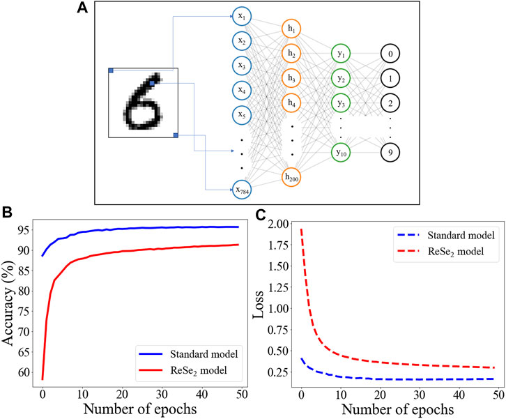
FIGURE 7. Application of ReSe2 RRAM for handwriting number recognition with MNIST dataset. (A) Schematic illustration of the ANN structure designed for the simulation. Comparison of (B) accuracy and (C) loss between models with standard and ReSe2 RRAM-based SGD optimizers.
In the simulation learning process, a customized SGD optimizer is designed to demonstrate the interference brought by the implementation of ReSe2 RRAM devices. After each epoch of training, the optimizer will calculate the gradient of the current weights. After that, the weights will be updated following Eq. 5.
Here
Here we consider the LTP/LTD processes are linear. The
The ANN with customized SDG optimizer is trained for 50 epochs. An ideal ANN with no customization is trained under the same conditions as a benchmark. After 50 epochs of training, the ANN based on ReSe2 RRAM devices achieved high recognition accuracy of 91.3%, which is comparable to the 95.71% accuracy of the ideal ANN model (Figure 7B). The loss of each model shows that neither of them exhibits over-fitting issue, which is desirable in the training process (Figure 7C). Note that the recognition accuracy of the ideal model used in this work is not as high as that in previously reported works. The main reason is that the model is not optimized for the specific application of handwriting recognition with MNIST dataset. By comparing the model with default parameters with the model implementing customized SDG optimizer, we can quickly assess the performance of the ANN using ReSe2 RRAM devices.
Conclusion
In summary, vertical crossbar MIM structure RRAM devices based on 2D ReSe2 have been found to exhibit excellent characteristics, e.g., stable multiple-step RESET when different levels of DC bias are applied. Furthermore, with the analog switching characteristic of the ReSe2, essential LTP and LTD behaviors are successfully mimicked. By implementing the physical properties, a Verilog-A compact model is designed to provide a standard method for future design of neuromorphic computing systems. In addition, the demonstration of a high handwriting recognition accuracy with ANN simulation shows the potential of the ReSe2 RRAM devices. The findings from our work provide additional insights into the application of 2D ReSe2 RRAM devices in the construction of brain-inspired neuromorphic computing systems.
Data Availability Statement
The original contributions presented in the study are included in the article/Supplementary Material, further inquiries can be directed to the corresponding author.
Author Contributions
YH and YG contributed equally to this work. The electrical characterization, model design and data process are done by YH. The device fabrication and material characterization are done by YG. XhW and RG provided instructions on measurement and fabrication. Y-FC gave instructions on the development of Verilog-A and ANN model. XyW wrote the SGD optimizer codes for the ANN model. JZ wrote part of the Verilog-A code.
Funding
This work was supported in part by the National Science Foundation (NSF) Grant #1809017. The authors acknowledge use of Texas Nanofabrication Facilities supported by the NSF NNCI award #1542159.
Conflict of Interest
Author Y-FC was employed by company Intel Corporation. Author XyW was employed by company Oracle Corporation.
The remaining authors declare that the research was conducted in the absence of any commercial or financial relationships that could be construed as a potential conflict of interest.
Publisher’s Note
All claims expressed in this article are solely those of the authors and do not necessarily represent those of their affiliated organizations, or those of the publisher, the editors and the reviewers. Any product that may be evaluated in this article, or claim that may be made by its manufacturer, is not guaranteed or endorsed by the publisher.
Acknowledgments
The authors appreciate Jo Wozniak and Anne Bowen of Texas Advanced Computing Centre (TACC) for 3D renderings.
References
Amirsoleimani, A., Alibart, F., Yon, V., Xu, J., Pazhouhandeh, M. R., Ecoffey, S., et al. (2020). In‐Memory Vector‐Matrix Multiplication in Monolithic Complementary Metal-Oxide-Semiconductor‐Memristor Integrated Circuits: Design Choices, Challenges, and Perspectives. Adv. Intell. Syst. 2, 2000115. doi:10.1002/aisy.202000115
Apte, A., Krishnamoorthy, A., Hachtel, J. A., Susarla, S., Yoon, J., Sassi, L. M., et al. (2019). Two-Dimensional Lateral Epitaxy of 2H (MoSe2)-1T′ (ReSe2) Phases. Nano Lett. 19, 6338–6345. doi:10.1021/acs.nanolett.9b02476
Bai, Y., Wu, H., Wang, K., Wu, R., Song, L., Li, T., et al. (2015). Stacked 3D RRAM Array with Graphene/CNT as Edge Electrodes. Sci. Rep. 5, 13785. doi:10.1038/srep13785
Cao, G., Meng, P., Chen, J., Liu, H., Bian, R., Zhu, C., et al. (2021). 2D Material Based Synaptic Devices for Neuromorphic Computing. Adv. Funct. Mater. 31, 2005443. doi:10.1002/adfm.202005443
Chang, Y.-F., Fowler, B., Chen, Y.-C., Zhou, F., Pan, C.-H., Chang, T.-C., et al. (2016). Demonstration of Synaptic Behaviors and Resistive Switching Characterizations by Proton Exchange Reactions in Silicon Oxide. Scientific Rep. 6, 1–10. doi:10.1038/srep21268
Du Nguyen, H. A., Yu, J., Xie, L., Taouil, M., Hamdioui, S., and Fey, D. (2017). “Memristive devices for computing: Beyond CMOS and beyond von Neumann,” in Proceedings of the IFIP/IEEE International Conference on Very Large Scale Integration. Abu Dhabi, United Arab Emirates, October 25 2017. VLSI-SoC IEEE. 1–10. doi:10.1109/vlsi-soc.2017.8203479
Ge, R., Wu, X., Kim, M., Shi, J., Sonde, S., Tao, L., et al. (2018). Atomristor: Nonvolatile Resistance Switching in Atomic Sheets of Transition Metal Dichalcogenides. Nano Lett. 18, 434–441. doi:10.1021/acs.nanolett.7b04342
Han, S.-T., Hu, L., Wang, X., Zhou, Y., Zeng, Y.-J., Ruan, S., et al. (2017). Black Phosphorus Quantum Dots with Tunable Memory Properties and Multilevel Resistive Switching Characteristics. Adv. Sci. 4, 1600435. doi:10.1002/advs.201600435
Hong, M., Zhou, X., Gao, N., Jiang, S., Xie, C., Zhao, L., et al. (2018a). Identifying the Non-identical Outermost Selenium Atoms and Invariable Band Gaps across the Grain Boundary of Anisotropic Rhenium Diselenide. ACS Nano 12, 10095–10103. doi:10.1021/acsnano.8b04872
Hong, X., Loy, D. J., Dananjaya, P. A., Tan, F., Ng, C., and Lew, W. (2018b). Oxide-based RRAM Materials for Neuromorphic Computing. J. Mater. Sci. 53, 8720–8746. doi:10.1007/s10853-018-2134-6
Jiang, S., Zhao, L., Shi, Y., Xie, C., Zhang, N., Zhang, Z., et al. (2018). Temperature-dependent Raman Spectroscopy Studies of the Interface Coupling Effect of Monolayer ReSe2 Single Crystals on Au Foils. Nanotechnology 29, 204003. doi:10.1088/1361-6528/aab3a4
Jiang, Z., Yu, S., Wu, Y., Engel, J. H., Guan, X., and Wong, H.-S. P. (2014). Verilog-A Compact Model for Oxide-Based Resistive Random Access Memory (RRAM)”. in Proceedings of the International Conference on Simulation of Semiconductor Processes and Devices (SISPAD). Yokohama, Japan, September 11 2014. IEEE. 41–44. 10.1109/SISPAD.2014.6931558 .
Kuzum, D., Yu, S., and Philip Wong, H.-S. (2013). Synaptic Electronics: Materials, Devices and Applications. Nanotechnology 24, 382001. doi:10.1088/0957-4484/24/38/382001
Li, Z., Chen, P.-Y., Xu, H., and Yu, S. (2017). Design of Ternary Neural Network with 3-D Vertical RRAM Array. IEEE Trans. Electron. Devices 64, 2721–2727. doi:10.1109/ted.2017.2697361
Lin, C.-Y., Chen, P.-H., Chang, T.-C., Chang, K.-C., Zhang, S.-D., Tsai, T.-M., et al. (2017). Attaining Resistive Switching Characteristics and Selector Properties by Varying Forming Polarities in a Single HfO2-Based RRAM Device with a Vanadium Electrode. Nanoscale 9, 8586–8590. doi:10.1039/c7nr02305g
Ma, X., Liu, Q., Xu, D., Zhu, Y., Kim, S., Cui, Y., et al. (2017). Capillary-force-assisted Clean-Stamp Transfer of Two-Dimensional Materials. Nano Lett. 17, 6961–6967. doi:10.1021/acs.nanolett.7b03449
Mcandrew, C. C., Coram, G. J., Gullapalli, K. K., Jones, J. R., Nagel, L. W., Roy, A. S., et al. (2015). Best Practices for Compact Modeling in Verilog-A. IEEE J. Electron. Devices Soc. 3, 383–396. doi:10.1109/jeds.2015.2455342
Moh, M., and Raju, R. (2018). Machine Learning Techniques for Security of Internet of Things (IoT) and Fog Computing systems”, in Proceedings of the International Conference on High Performance Computing & Simulation. Orleans, France. July 20 2018. HPCS IEEE, 709–715. 10.1109/HPCS.2018.00116 .
Mohanta, B. K., Jena, D., Satapathy, U., and Patnaik, S. (2020). Survey on IoT Security: Challenges and Solution Using Machine Learning, Artificial Intelligence and Blockchain Technology. Internet of Things 11, 100227. doi:10.1016/j.iot.2020.100227
Qiu, Z., Trushin, M., Fang, H., Verzhbitskiy, I., Gao, S., Laksono, E., et al. (2019). Giant Gate-Tunable Bandgap Renormalization and Excitonic Effects in a 2D Semiconductor. Sci. Adv. 5, eaaw2347. doi:10.1126/sciadv.aaw2347
Sahu, D. P., Jetty, P., and Jammalamadaka, S. N. (2021). Graphene Oxide Based Synaptic Memristor Device for Neuromorphic Computing. Nanotechnology 32, 155701. doi:10.1088/1361-6528/abd978
Sebastian, A., Le Gallo, M., Khaddam-Aljameh, R., and Eleftheriou, E. (2020). Memory Devices and Applications for In-Memory Computing. Nat. Nanotechnol. 15, 529–544. doi:10.1038/s41565-020-0655-z
Shen, Z., Zhao, C., Qi, Y., Xu, W., Liu, Y., Mitrovic, I. Z., et al. (2020). Advances of RRAM Devices: Resistive Switching Mechanisms, Materials and Bionic Synaptic Application. Nanomaterials 10, 1437. doi:10.3390/nano10081437
Shi, Y., Liang, X., Yuan, B., Chen, V., Li, H., Hui, F., et al. (2018). Electronic Synapses Made of Layered Two-Dimensional Materials. Nat. Electron. 1, 458–465. doi:10.1038/s41928-018-0118-9
Wang, T. Y., Meng, J. L., Chen, L., Zhu, H., Sun, Q. Q., Ding, S. J., et al. (2021). Flexible 3D Memristor Array for Binary Storage and Multi‐states Neuromorphic Computing Applications. InfoMat 3, 212–221. doi:10.1002/inf2.12158
Wong, H.-S. P., Lee, H.-Y., Yu, S., Chen, Y.-S., Wu, Y., Chen, P.-S., et al. (2012). Metal-Oxide RRAM. Proc. IEEE 100, 1951–1970. doi:10.1109/jproc.2012.2190369
Wu, X., Ge, R., Chen, P. A., Chou, H., Zhang, Z., Zhang, Y., et al. (2019). Thinnest Nonvolatile Memory Based on Monolayer h‐BN. Adv. Mater. 31, 1806790. doi:10.1002/adma.201806790
Wu, X., Ge, R., Gu, Y., Okogbue, E., Shi, J., Shivayogimath, A., et al. (2021). “Universal Non-volatile Resistive Switching Behavior in 2D Metal Dichalcogenides Featuring Unique Conductive-Point Random Access Memory Effect,” in Proceedings of the 2021 5th IEEE Electron Devices Technology & Manufacturing Conference (EDTM). Chengdu, China. April 11 2021. doi:10.1109/edtm50988.2021.9420947
Wu, X., Ge, R., Huang, Y., Akinwande, D., and Lee, J. C. (2020). Resistance State Evolution under Constant Electric Stress on a MoS2 Non-volatile Resistive Switching Device. RSC Adv. 10, 42249–42255. doi:10.1039/d0ra05209d
Yan, X., Pei, Y., Chen, H., Zhao, J., Zhou, Z., Wang, H., et al. (2019a). Self-Assembled Networked PbS Distribution Quantum Dots for Resistive Switching and Artificial Synapse Performance Boost of Memristors. Adv. Mater. 31, e1805284. doi:10.1002/adma.201805284
Yan, X., Zhao, Q., Chen, A. P., Zhao, J., Zhou, Z., Wang, J., et al. (2019b). Vacancy-Induced Synaptic Behavior in 2D WS2 Nanosheet-Based Memristor for Low-Power Neuromorphic Computing. Small 15, e1901423. doi:10.1002/smll.201901423
Zhang, W., Gao, B., Tang, J., Li, X., Wu, W., Qian, H., et al. (2019). Analog‐Type Resistive Switching Devices for Neuromorphic Computing. physica status solidi (Rrl) – Rapid Res. Lett. 13. doi:10.1002/pssr.201900204
Zhu, R., Liu, L., Song, H., and Ma, M. (2020). Multi-access Edge Computing Enabled Internet of Things: Advances and Novel Applications. Springer. Berlin, Germany. .
Keywords: RRAM, 2D material, ReSe2, neuromorphic computing, verilog-a, artificial neural network
Citation: Huang Y, Gu Y, Wu X, Ge R, Chang Y-F, Wang X, Zhang J, Akinwande D and Lee JC (2021) ReSe2-Based RRAM and Circuit-Level Model for Neuromorphic Computing. Front. Nanotechnol. 3:782836. doi: 10.3389/fnano.2021.782836
Received: 24 September 2021; Accepted: 03 November 2021;
Published: 19 November 2021.
Edited by:
Ying-Chen (Daphne) Chen, Northern Arizona University, United StatesReviewed by:
Vedarethinam Vadanasundari, Shanghai Jiao Tong University, ChinaJiyong Woo, Kyungpook National University, South Korea
Copyright © 2021 Huang, Gu, Wu, Ge, Chang, Wang, Zhang, Akinwande and Lee. This is an open-access article distributed under the terms of the Creative Commons Attribution License (CC BY). The use, distribution or reproduction in other forums is permitted, provided the original author(s) and the copyright owner(s) are credited and that the original publication in this journal is cited, in accordance with accepted academic practice. No use, distribution or reproduction is permitted which does not comply with these terms.
*Correspondence: Jack C. Lee, bGVlamNAYXVzdGluLnV0ZXhhcy5lZHU=
 Yifu Huang
 Yuqian Gu
 Xiaohan Wu1
 Jiahan Zhang
 Deji Akinwande