 Shima Hosseinzadeh
 Mehrdad Biglari
 Dietmar Fey
- Department Computer Science, Chair of Computer Architecture, Friedrich-Alexander-Universitat Erlangen-Nürnberg (FAU), Erlangen, Germany
Non-volatile memory (NVM) technologies offer a number of advantages over conventional memory technologies such as SRAM and DRAM. These include a smaller area requirement, a lower energy requirement for reading and partly for writing, too, and, of course, the non-volatility and especially the qualitative advantage of multi-bit capability. It is expected that memristors based on resistive random access memories (ReRAMs), phase-change memories, or spin-transfer torque random access memories will replace conventional memory technologies in certain areas or complement them in hybrid solutions. To support the design of systems that use NVMs, there is still research to be done on the modeling side of NVMs. In this paper, we focus on multi-bit ternary memories in particular. Ternary NVMs allow the implementation of extremely memory-efficient ternary weights in neural networks, which have sufficiently high accuracy in interference, or they are part of carry-free fast ternary adders. Furthermore, we lay a focus on the technology side of memristive ReRAMs. In this paper, a novel memory model in the circuit level is presented to support the design of systems that profit from ternary data representations. This model considers two read methods of ternary ReRAMs, namely, serial read and parallel read. They are extensively studied and compared in this work, as well as the write-verification method that is often used in NVMs to reduce the device stress and to increase the endurance. In addition, a comprehensive tool for the ternary model was developed, which is capable of performing energy, performance, and area estimation for a given setup. In this work, three case studies were conducted, namely, area cost per trit, excessive parameter selection for the write-verification method, and the assessment of pulse width variation and their energy latency trade-off for the write-verification method in ReRAM.
1 Introduction
Ever since the creation of the digital computing systems, the base of two has mostly been utilized for information processing and communication. Nevertheless, it is long known that a ternary representation of data, i.e., for each digit di of a number holds, e.g., di ∈ { − 1, 0, 1} or di ∈ {0, 1, 2}, offers advantages over the binary system in some aspects (Metze and Robertson, 1959; Avizienis, 1961; Parhami, 1470). One of the most attractive merits of using the ternary system is its capability of carrying out an addition operation in two steps, i.e., in O (1), regardless of the operand length [an example can be found in the work of Fey (2014)]. Using a binary data representation, this can be done only in O (log(N)) with a reasonable hardware effort. Furthermore, neural networks with ternary weights are much better than ones with binary weights and not much worse than ones with floating-point weights concerning the recognition accuracy, and they require much less storage capacity than neural networks with floating-point weights (Yonekawa et al., 2018).
However, realizing ternary states with binary storage elements requires two binary storage elements, e.g., flip-flops (Rath, 1975), making such designs immensely expensive. With the emergence of CMOS-compatible multi-bit capable memristive resistive random access memories (ReRAMs)1, this situation changed. This is achievable by ReRAMs because their resistive window can be splitted into quantized levels for having multilevel states (El-Slehdar et al., 2013). The idea of programming memristive devices into several resistance states was proposed, e.g., in the work of Kinoshita et al. (2007), in which the authors analyzed the application of a thin-film memristor as an N-level ReRAM element. Another approach, which was introduced by Junsangsri et al. (2014), uses two memristors to obtain three different states to handle ternary states instead of multiple quantized memristive levels but loses the advantage of saving one storage cell compared to multi-bit approach.
Using memristive devices for ternary arithmetic was first investigated by Fey (2014). On the basis of the work of Fey et al. (2016), the improvement in the energy-delay product and area for a ternary adder circuitry using multi-bit registers based on memristors compared to SRAM-based solutions was shown. The architecture can be further enhanced by using memristor-based pipeline registers that make it possible to use homogeneous pipelines for not only the addition operation but also the subtraction and multiplication operations instead of superscalar pipelines that use different pipeline paths for various operations (Fey, 2015). Although various proposals for ternary memristive circuits are now available in the literature, there is still a lack of sufficient ternary modeling at the circuit level to be able to use such components systematically and more easily than today in one’s own circuits.
Memory modeling enables architectural exploration and system integration of different memory technologies and design approaches. To ease the process of memory modeling, a need for a comprehensive modeling tool seems to be evident. Luckily, some high-precision open-source modeling tools such as CACTI (Wilton and Jouppi, 1996; Thoziyoor and Ahn, 2008), NVSim (Xiangyu Dong et al., 2012), and Destiny (Mittal et al., 2017) enable designers not only to utilize them with their original offered toolsets but also to build upon the current features for state-of-the-art modeling, which, in our case, is ternary memory modeling.
Research and development on non-volatile memories (NVMs) either require prototype chips, which are limited to a small portion of the entire design area, or a simulation tool that estimates energy, area, and performance of NVMs with different design specifications before the real chip fabrication. When designing a ternary system, researchers cannot benefit from any of the aforementioned solutions because there are no ternary memory chip fabrications and appropriate simulation tools have yet to be developed. Although the current most popular NVM simulation tools offer some design and estimation features, they still have limitations with respect to ternary memory design and accurate evaluation.
In this work, for the first time, to the best of our knowledge, a new ternary model has been developed that utilizes different reading and writing methods. Moreover, a comprehensive simulation tool for ternary memory modeling has been developed, which uses the NVSim (Xiangyu Dong et al., 2012) as its base. The main contributions of this work are as follows:
• Development of a comprehensive simulation tool for ternary memory modeling called “TReMo+”. On the one hand, the TReMo+ benefits from the methods and feature sets used by the most well-known memory simulation tools, namely, NVSim (Xiangyu Dong et al., 2012) and Destiny (Mittal et al., 2017), and on the other hand, it adds some more features for the first time ever.
• One of the unique features of the TReMo+ is that it supports the generic write-verification method for both reset and set operation, with the capability of overwriting average iteration, and different pulse width and voltage or current amplitude for consecutive pulses. This write method is made available for both the binary and ternary memory models.
• For the first time, TReMo+ introduced two new read methods, namely, serial and novel parallel read, which are configurable based on the desire of the user. The serial read method was adapted from the work of Mittal et al. (2017), and the novel parallel read approach was introduced in our previous work (Hosseinzadeh et al., 2020).
• Because the TReMo+ supports not only binary but also ternary memory modeling, the tool now enables users to choose optimization target for ternary memory (alongside with binary memory modeling), which could be area, latency, and energy.
Furthermore, we demonstrated the application of our model with three case studies. In addition to area cost per trit evaluation studied in our previous work (Hosseinzadeh et al., 2020), we present two further case studies in this work, namely, excessive parameter selections for the write-verification method and programming pulse width assessment. In the first case study, the impact of Incremental Step Pulse and Verify Algorithm (ISPVA) on delay and energy consumption is investigated to achieve more reliable writing operations and compared it to other known methods. These comparisons between different write schemes including the overhead and enhancements (as a trade-off analysis) are possible by using the presented model using the TReMo+ tool that we developed.
The TReMo+ modeling tool can assist researchers who are modeling systems in architecture-level tools such as gem5 (Binkert et al., 2011) by estimating performance, energy, latency, and area of the ternary ReRAM-based memory models. This tool also gives memory designers the ability to employ ternary logic based on ReRAM in their designs. The benefits of this work are not only limited to stand-alone ternary logic but also include exploiting new storage mechanisms and architectures. In other words, TReMo+ supports the use of innovative computing storage technology in own CMOS-based designs.
The rest of the paper is structed as follows: In Section 2, some basic information about the ReRAM will be presented, and different reading and writing methodologies on this memory will be studied. In Section 3, after having a deep overview of the state-of-the-art memory simulation tools, a thorough comparison among them will be reported. Section 4 is about implementation of the novel read and write methods in ReRAM devices, followed by Section 5, in which the results will be presented. Last, in Section 6, three case studies will be elaborated, and a brief conclusion will be presented in Section 7.
2 Preliminaries
2.1 ReRAM
Many of the NVM technologies, such as PCRAM and STTRAM, are designed on the basis of electrically inferred resistive switching effects. ReRAM is implemented by utilizing electro- and thermochemical effects, resulting in the resistance change of a memory architecture, in which a metal/oxide/metal layer stack is used to store data (Hosseinzadeh et al., 2020). In our confined variation, which is a bipolar ReRAM, a metal oxide layer (e.g., Ti O 2, Hf O 2) is sandwiched between two metal electrodes to store data. The value stored in the memory is dependent on the oxygen vacancy concentration of the metal oxide layer. When a voltage is applied to the two electrodes, conductive filaments (CFs) are either formed or ruptured, depending upon the voltage polarity. In case of CF formation inside the metal oxide, the top and the bottom of the electrodes are bridged, and the current can flow inside the CF. In this situation, the cell is considered to be in a low-resistance state (LRS), representing the value of “1”. Oppositely, when the CF is ruptured, the top and the bottom electrodes are disconnected and thus result in a high-resistance state (HRS) representing the value of “0” (Yang et al., 2008).
It has been proven by Xu et al. (2013) that the size of the CF has a direct relation with the value of the current, meaning that the cell resistance can be controlled by changing the strength of the CF. Therefore, it would be possible to program the middle-level resistance of ReRAM between the HRS and the LRS by manipulating the programming current and to establish by the multi-bit capability.
Figure 1 represents the physical behavior of a bipolar ternary ReRAM memory. As it can be seen in Figure 1A, by increasing the size of the CFs, the resistance is decreased, resulting in two distinct LRSs, namely, LRS1, and LRS2. On the other hand, as it can be seen in Figure 1B, by decreasing the size of the CFs, the resistance is increased, resulting in the HRS. Programming to intermediate states can be started from either the highest-resistance state (H2L programming) or the lowest-resistance state (L2H programming).
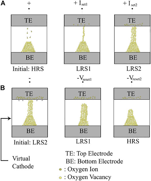
FIGURE 1. Multi-level switching in ternary ReRAM: (A) H2L and (B) L2H programming.
2.2 Read Methodologies in ReRAM
The normal read operations in ReRAM and many other NVM technologies are identical. The read operation can be done in two ways, in which both of them take advantage of the fact that NVMs have different resistances in LRS and HRS states. In the first method, a small voltage is applied on the bitline attached to NVM storage cell, and the current moving through the cell is measured. In the second method, a small current is sent out in the bitline, and in return, the voltage across the memory cell is measured. The methods are known as current sensing or voltage sensing, respectively. The response back from the cell comes in the form of voltage (or current), and afterward, it is compared against a reference voltage (or current). The comparison is done by utilizing a sense amplifier (SA) (Xiangyu Dong et al., 2012).
Depending on the resistance levels stored in one cell, the number of SAs varies. In the case of SLC (single-level cell or 1 bit per cell), it is sufficient to use one SA for the read operation (Xiangyu Dong et al., 2012), whereas in non-SLCs, the number of the SAs should be more than one, depending on whether the read operation is done in serial or in parallel.
2.2.1 Serial Read
Serial sensing for the non-SLC memories can be done by two methods. In our case, non-SLC memories consist of MLC (multi-level cell or 2 bits per cell for storing four states), TLC (triple-level cell or 3 bits per cell for storing eight states), and ternary (three states in 2 bits per cell) memories. The first method is the sensing model, which is based on the multi-step “sequential single reference”. This method is based on the non-linearity nature of charging and discharging resistance of the NVMs. Within the resistance change time, the SA captures samples from it (Xu et al., 2013). The second method is the binary search read out model, in which the number of read out iterations is based on the number of stored bits in the cell (Mittal et al., 2017).
2.2.2 Parallel Read
In the parallel sensing method, only a single step is needed, but the current (or voltage) is compared with multiple current (or voltage) references (Xu et al., 2013). On the basis of the work of Xu et al. (2013), the MLC parallel read circuitry is associated with seven sets of SA.
In our work, ternary read circuitry could be the binary search readout method or the parallel read method. We carry out two comparisons using the binary read approach for the ternary memory. For distinguishing the resistances in ternary memories with the parallel read approach, two SAs are enough.
2.3 Write Methodologies in ReRAM
A set operation is defined as switching between HRS and LRS, and reset is vice versa (Biglari et al., 2018). Because there is a large resistance variation, cell programming with verification could add an extra level of reliability (Higuchi et al., 2012). To control the cell programming in intermediate states, either the DC sweep (Grossi et al., 2016), write-verification (Higuchi et al., 2012; Song et al., 2013), or ISPVA (Higuchi et al., 2012) is applied, which could start from lowest- to highest-resistance state (L2H) or vice versa (H2L).
The ISPVA is based on a chain of increasing voltage pulses on the drain electrode during set operation, whereas during reset operation, this sequence of pulses is applied to the source terminal. After applying each pulse, a read verification is done to check whether the read current has reached the threshold value for the set and the reset operation. The algorithm stops when the threshold is reached (Pérez et al., 2018). Although single pulse benefits from shorter forming time by using high compliance and voltage parameters (Grossi et al., 2016), ISPVA offers a wide range of advantages including improvements in spatial process variation, more reliable writing, and higher endurance (Pérez et al., 2018; Pérez et al., 2019).
2.4 Trade-offs in Writing Parameter Selections
The high cycle-to-cycle and device-to-device variability in switching characteristics of ReRAM devices will result in excessive electrical stress on ReRAM cells during the worst case–based programming (Biglari et al., 2019). This contributes to a higher energy consumption as well as reduced reliability (Yu et al., 2012) and endurance (Song et al., 2013). To tackle this problem, novel structures have been proposed that intrinsically reduce this stress at the cell level (Linn et al., 2010; Biglari and Fey, 2017). Write-verification (Song et al., 2013; Higuchi et al., 2012) and feedback-based programming (Lee et al., 2017; Biglari et al., 2018) terminate the write operation after detecting that the device has reached the desired state.
In write-verification programming, this detection is done by reading the device between programming steps, whereas in feedback-based programming, the resistive state of the cell is monitored at real time during programming. The ISPVA method mentioned in the previous section is in the category of write-verification method. Both methods also enable multi-level programming of the ReRAM cells (Lieske et al., 2018; Puglisi et al., 2015). This work models a write-verification method that is the most common practice for memory design.
Although bearing the extra cost of the write-verification method is undeniable, it can be seen in other experiments that the ISPVA method was utilized both for SLC and MLC types of memory, mainly due its numerous advantages mentioned above (Pérez et al., 2018; Pérez et al., 2019).
A key capability of a memory model is to demonstrate how the observed behavior of a memory cell (in this case, ReRAM) at the device level will affect the overall behavior and performance characteristics of complete memories constructed with it.
In this case study, we study how write-verification parameter selection affects delay and energy consumption of the realized memory in relation to its endurance and reliability properties.
3 Simulation Tool
3.1 The NVSim Tool
To investigate early phases of NVM design, a simulator for ReRAM circuit level design is needed, so that the evaluation without any real-chip fabrication can be done. Among existing tools used in industry and academia for NVM estimation, the NVSim (Xiangyu Dong et al., 2012) and Destiny (Mittal et al., 2017) are the most popular ones.
The NVSim simulates some of non-volatile memristor–based memory technologies, such as phase-change memory, spin-transfer torque random access memory, and ReRAM. As an input, the NVSim takes device parameters and optimizes the circuit design and, as an output, evaluates the area, energy, and performance with the given design specification.
NVSim organizes chips using three main building blocks: bank, mat, and subarray. As shown in Figure 2, the top level building block in the hierarchy is the bank, and each bank consists of some mats, and last, subarrays are designed inside mats as the basic structure of a memory, in which they contain memory arrays and peripheral circuitry. The peripheral circuitry has SAs, a multiplexer (Mux), a decoder, and an output driver, and the overall cell layout is controlled by the access transistor. In Figure 3, the peripheral circuitry associated with the bitline of the subarray, used by NVSim, is depicted (Xiangyu Dong et al., 2012).
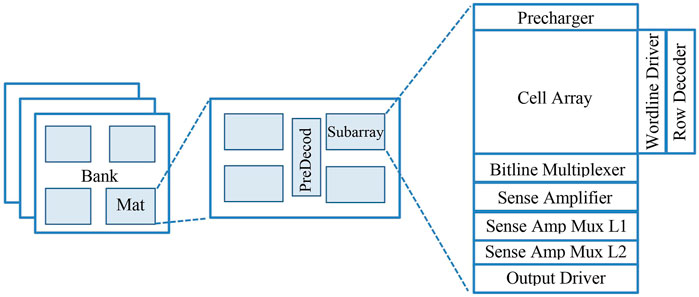
FIGURE 2. Memory array organization in NVSim (Xiangyu Dong et al., 2012).

FIGURE 3. Peripheral circuitry associated with bitlines in the NVSim.
The NVSim only models the SLC memories with regard to the submitted code. A more recent fork of NVSim, called Destiny, introduced a design evaluation of MLCs. In our work, a novel design for ternary memory simulation is implemented by heavily modifying the original NVSim code. The main focus of our work is internal sensing, and changes for ternary modification are done in the subarray level, especially in the peripheral circuitry, and then, the effects are evaluated in higher levels of the cell design. Needless to say, this work focuses on modeling of memories and not designing circuits. Therefore, we modeled the ternary model on the basis of the block diagrams. Describing the details regarding the building block of our models is out of scope of this work. However, for circuit detail of every module, the base of most of modules is described in the manuscript and guideline of CACTI (Wilton and Jouppi, 1996; Thoziyoor and Ahn, 2008) and some small parts in NVSim (Xiangyu Dong et al., 2012). Furthermore, our solution differs in further features that are outlined next.
3.2 Simulation Tools Comparison
Among many NVM simulation tools, NVSim (Xiangyu Dong et al., 2012) and Destiny (Mittal et al., 2017) are the ones offering the richest features. However, these tools lack certain essential features for more accurate results and for maintaining the fast-paced NVM technology. The present work addressed some of these issues by adding the missing features to the toolset.
For instance, NVSim only supports SLC design, whereas Destiny included MLC, allowing a cell to store 1 bit, 2 bits, 3 bits, etc. The present work introduced the support for ternary memory cells considering three states for the first time.
The support for the generic write-verification–based method that is capable of variant pulse width and variant current or voltage amplitude for both set and reset operation is another feature added in TReMo+, which was entirely absent in the NVSim. In addition, there are no verifications done when writing data, neither in reset before set nor in set before reset in NVSim, whereas in TReMo+, the verification is possible for both cases. In Destiny, only the write-verification method with fixed voltage and current is supported. Although not directly mentioned in the Destiny paper, it is evident that, in latency and energy calculation formulae, time pulses for voltage and current are equal, which is not the common write method for memories. For more realistic and accurate results, in TReMo+, we added the enhanced variant of write-verification method for both reset and set operations, namely, 1) with the dynamic voltage levels and pulse widths and 2) current levels with the variant pulse widths. Moreover, TReMo+ has two read methods, namely, serial and the novel parallel read methods, whereas in Destiny, only serial read is available.
4 Implementation and Methodology
4.1 Sense Amplifier Read Circuitry
To adapt the NVSim SA read circuitry to the ternary memories, it is necessary to take both read methods into consideration, specifically the serial read and the parallel read.
In the serial read, there are no modifications needed to the internal SA block of the original NVSim. However, the total number of SAs are halved, due to the halved number of columns in ternary memory. It is notable to mention that, for the serial read, as shown in Figure 4, the maximum number of read iterations should be two times.
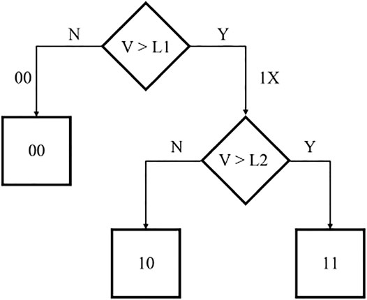
FIGURE 4. Serial read model for ternary memory.
In contrast, the parallel read requires some adjustments in the NVSim SA read circuitry. To store three values in one cell, it is necessary to have a trit cell; we therefore added an extra SA coupled with the existing SA so that it would be possible to read from a cell concurrently. Storing ternary data requires at least three distinguished levels of resistance. To accomplish this, at least two sense SAs with different voltage references are required. Therefore, one bitline should be connected to two SAs.
The general idea of dividing and distinguishing the resistance level in parallel read circuitry is demonstrated in Figure 5. As a result, Vref1 and Vref2 should adhere to the following rules: 1). To prove this design, the truth table is shown in Figure 5B.
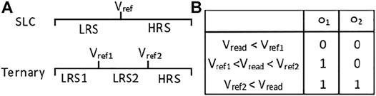
FIGURE 5. (A) Resistance level in ternary memory. (B) Truth table for parallel ternary read.
The original SA in NVSim is based on the SA used in the CACTI (Thoziyoor and Ahn, 2008) tool, which is voltage-based. Therefore, we kept this module unchanged. In case of current sensing, an I-V converter is needed, which is responsible for converting the current running in the bitlines to voltage before passing through the SAs. Because two SAs work simultaneously, one I-V converter is sufficient to be shared among two SAs in case of current sensing depicted in Figure 6B.
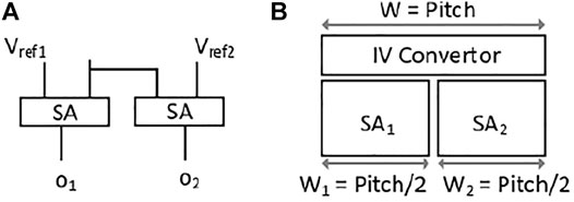
FIGURE 6. (A) SA circuitry for ternary memory in parallel read. (B) The ternary SA block layout. Pitch is the maximum allowed width for one SA layout in NVSim.
4.2 Write Operation Modeling for Single-Level Cell and Non–Single-Level Cells
4.2.1 Single Write
In non-crossbar structures, the write pulse is applied once to the cell, assuming that the cell will be written in only one single pulse. Writing to the cells is performed in two steps. First, the row decoder applies the row address to latch the data from a row of the ReRAM subarray module into the SAs. Second, after the data become latched, the column address is applied, and the read or write access will be performed. Figure 7 shows the write path for a single cell. The latency is calculated by summing the worst-case latency of reset and set pulse, the maximum value among decoder latency, and the summation of the column decoder latency (calculated by summation of latency of bitline Mux decoder, SA Mux decoder level 1 and level 2 modules) and the latency of other modules in the write path (calculated by summation of latency of bitline Mux, SA Mux level 1 and level 2).
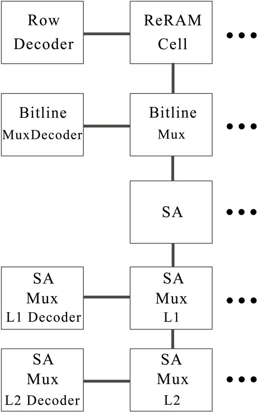
FIGURE 7. The write path for one cell at the subarray level.
In crossbar structures, because set and reset operations cannot be performed simultaneously, two methods for write operations are available; first, having a separated set and reset operation called “reset before set” or ”set before reset” method and, second, in which all the cells in the selected row are erased before a selective set operation is carried out. This method is called the “erase before set” or “erase before reset” method (Xiangyu Dong et al., 2012).
4.2.2 Verification After Single Write
Another write scheme that is utilized and modeled in this work is the verification after single write. The latency of any cell type (crossbar or non-crossbar) with the “write and verification” scheme is higher than the “without verification” one. The read latency itself comes from the latency of every module in the read path sequentially, for instance, SAs, bitline Muxes, and different multiplexers that come after the SAs or the decoders. From the write energy perspective, in the “write and verification scheme”, the energy consumed for the verification, specifically in the cell and the SA, are added to the write energy. Therefore, the write energy in this scheme is higher than that of the “write without verification” scheme.
4.2.3 The Write-Verification Method
There are two variants of write-verification methods that have been modeled in this work. The first variant is based on the write method used by Xu et al. (2013). On the basis of this variant of write-verification method, first, the device is initialized to reset state by a single pulse followed by an iterative sequence of set and verification pulses until the device has reached the desired resistive level (Figure 8A) or vice versa. The second variant is based on the write method used by Pérez et al. (2017). On the basis of this variant of write-verification method, first, the device is being initialized to reset state with a sequence of iterative reset and verification pulses. Then, it is programmed to the desired resistive state by a sequence of iterative set and verification pulses (Figure 8B).
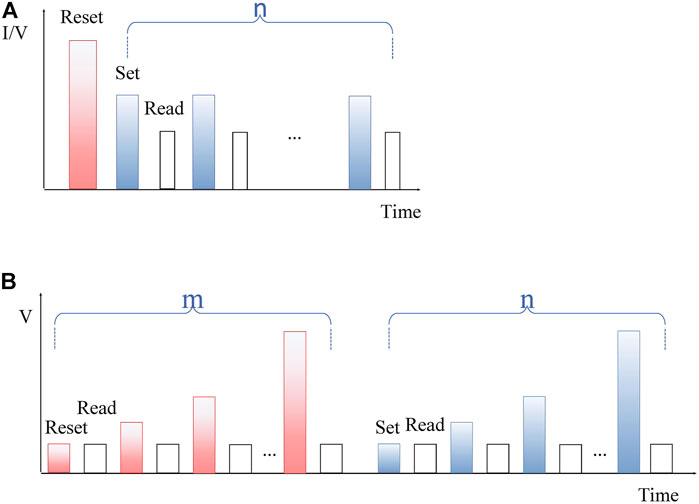
FIGURE 8. (A) The first variant of write-verification model (reset before set). (B) The second variant of write-verification model (ISPVA).
The average energy for single-pulse–based reset (first variant) is calculated by the following:
The amounts of energy consumed during the sequence of program and verification pulses for the reset operation in second variant and the set operation for both variants are calculated by either (3) or (4) as follows. It is considered that the average number of iterations for set and reset operations is assigned to variable “n” and “m”, respectively.
If the set or reset operation holds the current source, then the energy is calculated by the following:
If the set operation holds the voltage source, then energy for the set operation is calculated by the following:
PV = [v1, v2, … ,vn|vm] consists of a sequence of voltages in the write-verification method for the set or reset procedure.
PI = [I1, I2, … ,In|Im] consists of a sequence of currents in the write-verification method for the set or reset procedure.
PT = [t1, t2, … ,tn|tm] consists of a sequence of pulse widths of current or voltage pulses for the set or reset procedure.
Vdrop is the voltage dropping on the device due to the transistor connected to the cell while reading or writing.
The total required energy for writing is as follows:
The total latency for writing for the first variant write-verification is calculated by the following:
The total latency for writing for the second variant write-verification is calculated by the following:
4.3 Analysis of Single-Level Cell and Parallel Ternary
In this section, an architecture for ternary memory in the subarray level is modeled and evaluated in terms of area, latency, and dynamic energy.
4.3.1 Ternary Area Consumption
Figure 9 shows the SLC and the ternary memory in parallel read models in one frame. Given an SLC memory with the capacity specified by the product of the number of rows and columns, represented by the color black, a ternary memory with the same capacity is compared to it using the color red.
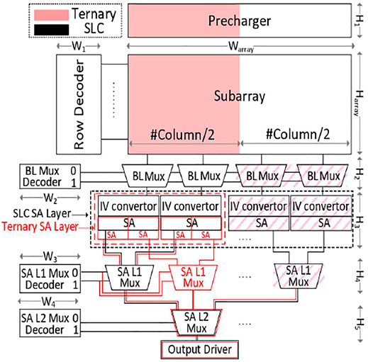
FIGURE 9. The peripheral circuitry for SLC memory (black bordered modules) and the proposed ternary memory (red bordered modules) in parallel read.
It can be seen that, in the parallel ternary memory, there has been some modifications, when compared to the SLC memory. The first change is the number of columns is halved in the subarray because each cell is capable of storing a trit. Subsequently, the width of the precharger is also halved for the same reason mentioned above. Moving forward to the layers below, the number of bitline multiplexers is halved, caused by the reduced number of columns. In the SA layer, the total number of internal SAs is kept unchanged, whereas the width of the SA layer is halved. It is also notable to mention that the height of each internal SA is slightly longer than that of SLC, but the effect of this is neglectable in the SA layer because the height of the I-V converter is dominant. In the next layer, namely, SA multiplexer level 1, the number of multiplexers has not changed, obviously because the number of SAs in the previous layer was kept constant. The same logic applies to the SA multiplexer level 2, and therefore, the total number is kept unchanged.
To estimate the area of each peripheral circuitry component, each component is delved into the actual gate-level logic design considering the height and width of each gate as it is also done in NVSim and CACTI. The height and width of each gate is dependent on the optimization target as we have three different types of transistors (latency-optimized, balances, and area-optimized) with different sizes. When calculating the total area at the subarray level in SLC memory, the following formulas are used (8) (9).
H1, H2, H3, H4, H5, and Harray are the height of precharger, bitline Mux, SA layer, SA Mux level 1, SA MUX level 2, and subarray modules, respectively, as depicted in Figure 9. W1, W2, W3, W4, and Warray are the width of row decoder, bitline Mux decoder, SA Mux decoder level 1, SA Mux decoder level 2, and subarray modules, respectively, as depicted in Figure 11. The total area is calculated by multiplication of the total height and the width. When evaluating the area consumption of the ternary memory with parallel read mode, all the heights and widths measurements are the same, except for Warray, which is halved, and the height of the SA. As a result, the total subarray area of the SLC memory is almost two times greater than that of the ternary memory.
In the case of ternary memory with serial read mode, there are some minor changes when compared to ternary memory with parallel read mode. First, the number of SAs is halved, whereas the width of each SA is doubled, keeping the total width of the SA layer unchanged. Second, the number of SA multiplexer level 1 and level 2 is halved because of the decreased number of SAs in the previous layer.
4.3.2 Ternary Latency
The latency calculated for the components is based on RC analysis and the simplified version of Horowitz’s timing model that is used in the NVSim tool (Xiangyu Dong et al., 2012) .
In this formula, α is the slope of the input, β = gmR is the normalized input transconductance by the output resistance, and τ is the RC time constant. When comparing the latency of the SLC memory cell with the ternary memory cell, some differences in the latency of each component can be found.
Row decoder is the first component with halved latency. The reason is that the number of subarray columns is halved, which results in halved wordline capacitance that is loaded to the row decoder.
Bitline multiplexer decoder is another component with halved latency, when compared to that of SLC. The capacitance loaded to this module comes from the capacitance of the wordline and the pass transistors of the multiplexers, and they are both halved. The same reason applies to the SA multiplexer level 1 and level 2 decoders. The total decoder latency is calculated by finding the maximum latency of the modules mentioned above, resulting in halved decoder latency.
When reading from the memory cell, the total read latency is the summation of the decoder latency, the bitline delay, and the delay of multiplexers through the read path. In the case of ternary memory with parallel read mode, the total read latency is less than that of SLC due to the halved decoder latency mentioned above, leaving the other latency values unchanged. However, in ternary memory with serial read mode, in addition to the halved decoder latency, SAs latency is doubled because binary search reading should be done at least twice. The comparison between the ternary memory with serial read mode and parallel read mode is also an interesting matter, because the read latency of the ternary memory with parallel read mode is lower than that of serial one. It can be justified that parallel read sensing is done in parallel with the use of the SA, whereas in serial read mode, two times more comparisons are needed in the worst-case scenario.
If we put the write latency under scrutiny, then we realize that the latency of the ternary cell is higher than that of SLC because the programming ternary cells need more write iterations than SLC. When comparing the write latency of the ternary memory with parallel read mode with that of the serial one, the write latency in the parallel mode is lower due to lower read latency in the parallel mode during the writing program by write-verification compared to the serial read.
4.3.3 Ternary Energy Consumption
The energy consumption comparison is done in this section between the ternary memory and the SLC memory type. The dynamic energy and leakage power consumption can be modeled as follows:
The dynamic energy of the precharger is halved because of the halved number of columns, which is caused by dividing the capacitance of the wordline by two. Dynamic energy of other modules including the decoders of the bitline multiplexers, row decoder, and SA level 1 and level 2 decoders is also halved for the exact same reasons mentioned above. The read dynamic energy consumed in SAs is the same in both cases because they have the same number of SAs. The dynamic energy of bitline multiplexer is unchanged; although the load capacitance of the two SAs connected parallel to it is doubled, the number of columns is halved.
Cell read energy is also lower in ternary memory, because, first, read pulse is not considered in the calculation and, second, the number of columns in the cell is halved compared to that of SLC. When reading from the ternary memory cell, the read dynamic energy is calculated by adding all dynamic energy of the active components mentioned above and cell read energy in the read path. In parallel read, sensing is done in parallel with the use of SA, whereas in serial read, two times more comparisons are needed in the worst-case scenario. As a result, the read energy consumption during serial read is higher than that of the parallel variant.
For a write operation on the ternary memory cell, the write dynamic energy is the sum of all active modules mentioned above plus write dynamic energy of the write path depending upon the writing method. When the write-verification method is used for writing data on a ternary cell, it will definitely need more iterations compared to the single-pulse method, resulting in higher write energy in ternary memory. It can therefore be concluded that the total dynamic energy in ternary is greater than SLC, despite the number of columns in SLC being two times more. It is worth to consider that the write energy for the ternary memory with parallel read mode is higher than that of the ternary memory with serial read mode because the two SAs are used for concurrent sensing passing through the bitline multiplexer that doubles the capacitance.
If the reset dynamic energy and the set dynamic energy were analyzed separately assuming the first variant of write-verification, the reset dynamic energy in SLC would be greater than in the ternary memory because the number of columns in SLC is higher than in the ternary memory. However, because the number of iterations in ternary memory is higher than SLC, the set dynamic energy in this memory is greater than SLC, outweighing the number of columns in ternary.
Regarding the cell leakage, the total leakage in SLC is higher than that of the ternary memory. The reason behind this is the effect of the dominant precharger leakage in SLC on the total leakage.
5 Results
5.1 Single-Level Cell ReRAM With Write-Verification
The motivation for this section is to demonstrate some additional enhancements on SLC memory models, previously modeled in NVSim, such as the verification after single write or first variant of write-verification method by considering the overhead of the verification controller as input.
In cases of verification-based write method, a finite state machine (FSM) is required to control the write scheme. For instance, when a write voltage is applied, the state machine is utilized to verify the current whether the write was successful followed by iteration termination or the voltage should still be increased. The overhead values of this state machine, including the energy, latency, and area, are technology dependent; therefore, these values can be estimated by the synthesis results of the desired controller. The FSM overhead values, including the area, latency, and energy overhead, are then given as an input to the simulator for a more accurate result. Therefore, TReMo+ is capable of getting the overhead of write driver as an input to make estimated values closer to real fabricated chip values. However, our evaluations for the memory arrays are based on the IHP cell settings, and they also do not have a write-driver to produce the pulse trains. The pulse trains in IHP company are produced with a computer-based system called RIFLE SE. Therefore, even the IHP researchers do not have the overhead values for producing the consecutive pulses, and as a result, the overhead of the control circuitry is not considered in the results.
The SLC ReRAM model used for this section is based on a 0.18-µm 4-Mb MOS-accessed ReRAM prototype chip (Sheu et al., 2011). According to Xu et al. (2013), the set and reset pulse duration were set to 5 ns
Table 1 contains a thorough comparison of 1T1R and crossbar architecture, each with and without verification after the writing scheme with different underline physics.
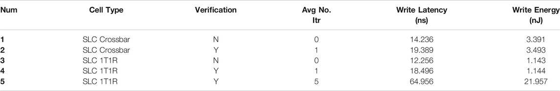
TABLE 1. The effect of single verification and multiple verification on latency and energy of crossbar and SLC 1T1R architecture. Item number 1 does not have the verification method after writing, whereas item number 2 has only one iteration of verification. Last, item number 3 has verification with five times iteration. The reason behind different numbers of iteration is due to different underlying physics.
As it can be seen, the verification method after writing to the cells has increased the write energy and the latency based on the explained reasons in Section 4.3. The write latency has increased at least by 42%.
5.2 Ternary Memory With Serial and Parallel Modes Vs. Single-Level Cell Memory
The experimental results shown in Table 2 are based on the prototype chip of Sheu et al. (2011) with the first variant of write-verification method for different memory models including SLC and ternary memroy with serial and parallel mode. It is assumed that the average number of iterations set in the first variant of write-verification method for SLC and ternary model are 5 and 12, respectively. In addition, the projected results for the ternary memory in serial and parallel modes are compared with the SLC memory in Table 2. As it can be seen in Table 2, the parallel read has a lower read latency in comparison with the serial read while keeping the overhead to a minimum level.
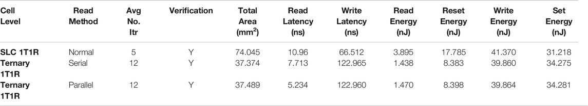
TABLE 2. 1T1R SLC memory vs. ternary memory with serial and parallel read based on the first variant of write-verification scheme.
In MLC mode, the ReRAM prototype chip has a write latency of 160 (Sheu et al., 2011). Using first variant of write-verification method with number of set iterations as 12 in TReMo+, we observe the write latency for ternary memory with serial and parallel modes that are 122.965 and 122.960 ns, respectively, as shown in Table 2. Thus, our ternary memory projected to have lower write latency than the MLC version of the prototype chip as expected within an acceptable error rate.
6 Case Studies
6.1 Write-Verification Parameter Settings Trade-offs
The work described in this subsection models the first variant of the write-verification method, which is explained in Section 4.2.3, and investigates the trade-off, which is explained in Section 2.4. The write-verification setting determines the write energy and write latency.
In this case study, we examine how the selection of the write-verification parameter affects the delay and the energy consumption of the realized memory in relation to its endurance and reliability properties. For the evaluation, the results from Pérez et al. (2017) are used as reference for our simulated data with TReMo+. The paper contains measurement data concerning the average number of programming iterations, the set voltage, and the voltage step acquired from various experiments on real ReRAM devices programmed using ISPVA. These devices were made by IHP2. The known device configuration from Pérez et al. (2017) served as inputs to our simulation tool. The write latency, the write energy, and the set energy at the chip level were collected from the output of the simulator. As shown in Table 3, by incrementing the voltage step, both the write latency and the spent energies for set and resetting of the device decrease subsequently. As a result, this study shows how the advancement of the device level, e.g., a still sufficient lower iteration number, can actually affect the actual design of memories. Therefore, the conveyed idea is that, for the minimum write latency and energy, the voltage step should be high. However, this is not the ultimate consideration because cell reliability and endurance after writing should also be examined, and these features can be negatively affected by large voltage steps.
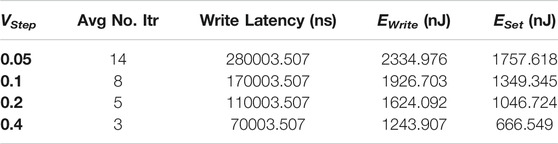
TABLE 3. The impact of ISPVA settings on latency and energy of the total memory.
With regard to the experiment done by Pérez et al. (2017), two important results were presented: 1) On the basis of Figure 10, by incrementing the voltage step, the number of cells willing to be set within the expected current threshold (the current threshold is the current threshold condition for the set operation in ISPVA) will decrease from ∼80%−90% to ∼ 60%. In other words, cells will be set with only one current peak when the voltage step is low, whereas in the opposite case when the voltage step is high, two current peaks appear (Figure 10). Quantization of the conduction is inherent to the CF, and therefore, it is always there. However, this behavior of the memory cell is due to the increase of the voltage step, and the overstress on the sample makes the conduction “jumping” to the next level of quantization, which means to a conduction level coherent with two CFs as it was observed and found by Pérez et al. (2017). It was demonstrated by Pérez et al. (2017) that, in lower-voltage steps, only one CF forms in the cell, whereas in higher-voltage steps, two separate CFs are formed or in other words the device is overset. 2) The carried-out cycling experiment on programmed cells with various voltage steps shows that the cells that are set with lower-voltage steps tend to be more stable than those with higher-voltage steps, making them only partially stable. The reason behind this instability is that, in higher voltages, two filaments are involved (or overset behavior) in the process of switching, making the reliability fragile (Pérez et al., 2017).
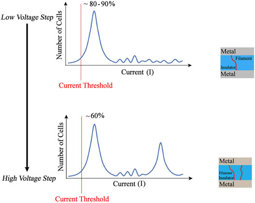
FIGURE 10. Current distribution for set operation with incremental voltage step. In the top curve, a lower incremental step is used as in the bottom. This figure is depicted based on Figure 6 in the work of Pérez et al. (2017).
It can be concluded that, for writing with the write-verification method (in this experiment, for the ISPVA method), there should be a trade-off when choosing an appropriate voltage step. The voltage step should not be too large to jeopardize the stability and, at the same time, should not be too low to increase the cells energy consumption.
6.2 Programming Pulse Width Assessment Trade-off
The work presented in this subsection models the second variant of the write-verification method, which is explained in Section 2.4. In this case study, we first verify that the results from TReMo+ correspond to the data at the cell level from IHP, and then, we examine how the programming of different pulse widths at the cell level affects the write energy and write latency at the chip level.
For this study, the results at the cell, such as the average iteration number for set and reset operation and the reset and set voltage for different pulse widths at the cell level, are extracted from the work of Perez et al. (2020). Besides, those data at the cell level and the IHP device configuration, such as 4 Kbit, read pulse width, and HRS and LRS values, given by Perez et al. (2020), are used as input to the simulation tool. As a result, the energy and latency at the cell and chip levels are collected from the output of the simulator.
For the first assessment, five different pulse widths—50 ns, 100 ns, 500 ns, 1 µs, and 10 μs—for both reset and set in ISPVA operation were utilized. Figure 11 depicts the trend of energy at the cell level for set (S_E_Cell), reset (RS_E_Cell), and read energy (RD_E_Cell_for_Rs, RD_E_Cell_for_Rs). Furthermore, we show in Figure 11 the read energy on the chip level for read (RD_E_total), reset (RS_E_total), and set (S_E_total). The data from TReMo+ at the cell match with the data at the cell level from IHP (Perez et al., 2020). Read energy at the cell and chip levels for set and reset operation is independent of the set and reset pulse width. However, reset and set energy at the cell and chip levels are increasing by the growth of pulse width. It is also evident that the reset energy is higher than the set energy both at the cell level and the chip level. It is validated that TReMo+’s result matches that of IHP’s at the cell level. In addition, TReMo+ also estimates the write latency and write energy at the chip level.

FIGURE 11. Average energy required to do reset (blue dots) and set (red dots) operations, read energy for set and reset, and total read on a single 1T1R ReRAM cell and 4 Kbit ReRAm memory arrays.
In the second assessment, TReMo+ was executed using different ordered pairs of the reset and set pulse widths. The ordered pairs are consist of the total combination of 50 ns, 100 ns, 500 ns, 1 µs, and 10 μs for set and 50 ns, 100 ns, 500 ns, 1 µs, and 10 μs for reset, making 25 cell configurations. These are used to evaluate the effect of different pulse widths on the energy and latency at the chip level and the best points in terms of the write energy and write latency. Needless to say, TReMo+ is capable of evaluating any pulse width given as an input. Therefore, there is no limitation to use our tool for any pulse width. Furthermore, for this case study, we utilized the experimental data at the cell level from the IHP company available in the work of Perez et al. (2020). Because of some limitation in producing a pulse width smaller than 50 ns for their experiments, they did not assess pulse width smaller than 50 ns in their analysis.
As it is depicted in Figure 12, the best point from write energy perspective belongs to 50 ns for reset and set pulse width. However, the lowest write latency belongs to 100 ns for reset pulse width and 500 ns for set pulse width, as depicted in Figure 13. Furthermore, as it can be seen in Figure 12, when increasing the set pulse width while keeping the reset pulse width fixed, the write latency will grow in each iteration. However, in this situation, the write energy will fall up to the third point but then starts to increase from the fourth point onward as depicted in Figure 12. As a result, the lowest write energy point among every five points is the third one. This shows the obvious trade-off between write latency and energy latency.
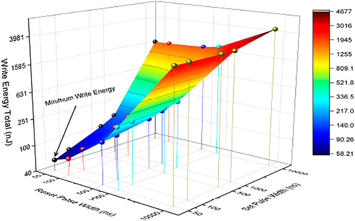
FIGURE 12. Write energy over different pulse widths.
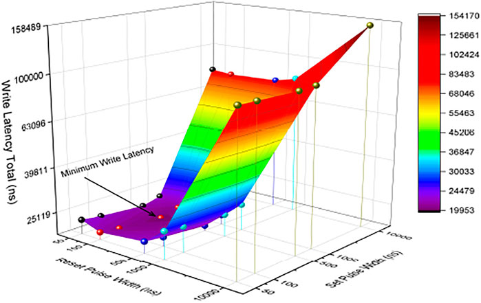
FIGURE 13. Write latency over different pulse widths.
On the basis of the retention and the reliability test in the work of Perez et al. (2020), there is no reliability issue for different combinations of reset and pulse width, except for that of 50 and 50 ns for reset and set pulse width, due to longer ending tail in Figure 3 in the work of Perez et al. (2020). That means, on the basis of the experimental results, although 50 ns for both reset and set pulse width shows the best write energy, 100 ns for reset and 50 ns for set pulse width with the second minimum write energy seems to be the best point for programming the cell with ISPVA with no reliability issue. Having discussed this, still a trade-off would exist to determine which programming pulse width ensures the lowest energy and the most reliable operation.
6.3 Area Cost per Trit
Cost per bit is one of the most important aspects when modeling a novel memory technology. Some memory design goals, such as technology scaling, chip yield enhancement, and cell structure modernization, all point toward reducing cost per bit of a memory chip.
When adapting the MLC memory for ternary memory design, the issue of area arises in a sense that is based on Section 4.1. Ternary memory does not require any decoders for the reading operation, whereas MLC needs at least seven sets of SA and an extra decoder (Xu et al., 2013). The results in Table 4 also prove that the area per trit in the ternary memory is the most optimal case.
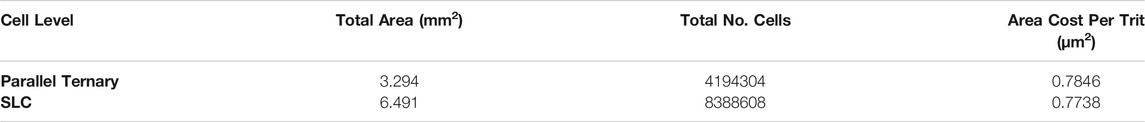
TABLE 4. Cost per trit.
According to Xu et al. (2014), to calculate cost per trit, area and fabrication costs are the most important factors. On the basis of the above explanation and assuming that fabrication costs in MLC and ternary memory are the same, a lower cost per trit in comparison to the MLC counterpart is given because the ternary memory has a smaller area. The experimental results shown in Table 4 are based on the same settings utilized in Section 6.2 but for 1-Mb memory chip capacity. The number of cells calculated in Table 4 is total number of cells of simulated complete array for the given setting.
7 Conclusion
In this paper, a new memristor-based ternary memory model was modeled that benefits from optimized reading and writing methods. Alongside the serial read method, the parallel read for the ternary memory model was modeled for the first time, which made the read latency lower than its rival and, at the same time, kept the overhead to a minimum. The writing method of choice in this paper was the write-verification method, which offered more reliable writing operation, compared with the single-pulse method.
Moreover, some case studies were presented for proving the usefulness and versatility of the model, including parameter selection for write-verification method and their ramifications on energy and latency, programming pulse width assessment and its trade-off in energy and latency, and a study on area cost per trit proving that the ternary case offers the most optimal solution in terms of area consumption.
Finally, to ease the process of ternary memory development by researchers and manufacturers, a comprehensive tool was developed that is capable of performing energy, performance, and area estimation for a given setting.
Data Availability Statement
The original contributions presented in the study are included in the article; further inquiries can be directed to the corresponding author.
Author Contributions
Conceptualization: SH and MB; Implementation and experimental evaluation: SH; Investigation: SH; Methodology: SH; Visualization: SH; Writing - original draft: SH; Manuscript revision, review, and editing: SH, MB, and DF.
Conflict of Interest
The authors declare that the research was conducted in the absence of any commercial or financial relationships that could be construed as a potential conflict of interest.
Publisher’s Note
All claims expressed in this article are solely those of the authors and do not necessarily represent those of their affiliated organizations or those of the publisher, the editors, and the reviewers. Any product that may be evaluated in this article, or claim that may be made by its manufacturer, is not guaranteed or endorsed by the publisher.
Acknowledgments
Authors would like to thank Eduardo Pérez from IHP for his valuable feedback and suggestions.
Footnotes
1The term memristor and ReRAM are used in this paper interchangeably.
2Innovations for High Performance Microelectronics.
References
Avizienis, A. (1961). “Signed-digit Numbe Representations for Fast Parallel Arithmetic,” in IEEE Trans. Electron. Comput. (IEEE), 389–400. doi:10.1109/tec.1961.5219227EC-10
Biglari, M., and Fey, D. (2017). “Memristive Voltage Divider: A Bipolar Reram-Based Unit for Non-volatile Flip-Flops,” in Proceedings of the International Symposium on Memory Systems, 217–222. doi:10.1145/3132402.3132432
Biglari, M., Lieske, T., and Fey, D. (2018). “High-endurance Bipolar Reram-Based Non-volatile Flip-Flops with Run-Time Tunable Resistive States,” in Proceedings of the 14th IEEE/ACM International Symposium on Nanoscale Architectures, 19–24. doi:10.1145/3232195.3232217
Biglari, M., Lieske, T., and Fey, D. (2019). Reducing Hibernation Energy and Degradation in Bipolar ReRAM-Based Non-volatile Processors. IEEE Trans. Nanotechnology 18, 657–669. doi:10.1109/tnano.2019.2922363
Binkert, N., Beckmann, B., Black, G., Reinhardt, S. K., Saidi, A., Basu, A., et al. (2011). The Gem5 Simulator. SIGARCH Comput. Archit. News 39, 1–7. doi:10.1145/2024716.2024718
El-Slehdar, A. A., Fouad, A. H., and Radwan, A. G. (2013). “Memristor-based Balanced Ternary Adder,” in 2013 25th International Conference on Microelectronics (ICM), 1–4. doi:10.1109/icm.2013.6735002
Perez, E., González Ossorio, Ó., Dueñas, S., García, H., and Wenger, C., “Programming Pulse Width Assessment for Reliable and Low-Energy Endurance Performance in Al: Hfo2-Based Rram Arrays,” Electronics, 2020.
Fey, D., Reichenbach, M., Söll, C., Biglari, M., Röber, J., and Weigel, R. (2016). “Using Memristor Technology for Multi-Value Registers in Signed-Digit Arithmetic Circuits,” in Proceedings of the Second International Symposium on Memory Systems, 442–454. doi:10.1145/2989081.2989124
Fey, D. (2015). Ternary Arithmetic Pipeline Architectures Using Multi-Bit Memristors. Future Comput., 1–6.
Fey, D. (2014). Using the Multi-Bit Feature of Memristors for Register Files in Signed-Digit Arithmetic Units. Semicond. Sci. Technol. 29, 104008. doi:10.1088/0268-1242/29/10/104008
Grossi, A., Zambelli, C., Olivo, P., Miranda, E., Stikanov, V., Walczyk, C., et al. (2016). Electrical Characterization and Modeling of Pulse-Based Forming Techniques in RRAM Arrays. Solid-State Electro. 115, 17–25. doi:10.1016/j.sse.2015.10.003
Higuchi, K., Iwasaki, T., and Takeuchi, K. (2012). “Investigation of Verify-Programming Methods to Achieve 10 Million Cycles for 50nm Hfo2 Reram,” in 2012 4th IEEE International Memory Workshop, 1–4. doi:10.1109/imw.2012.6213665
Hosseinzadeh, S., Biglari, M., and Fey, D. (2020). “Tremo: A Model for Ternary Reram-Based Memories with Adjustable Write-Verification Capabilities,” in 2020 23rd Euromicro Conference on Digital System Design (DSD), 44–48.
Junsangsri, P., Lombardi, F., and Han, J. (2014). “A Memristor-Based Tcam (Ternary Content Addressable Memory) Cell,” in 2014 IEEE/ACM International Symposium on Nanoscale Architectures (NANOARCH), 1–6. doi:10.1109/nanoarch.2014.6880478
Kinoshita, K., Tsunoda, K., Sato, Y., Noshiro, H., Yamazaki, Y., Fukano, T., et al. (2007). “Reduction of Reset Current in Nio-Reram Brought about by Ideal Current Limiter,” in 2007 22nd IEEE Non-Volatile Semiconductor Memory Workshop, 66–67. doi:10.1109/nvsmw.2007.4290583
Lee, A., Lo, C.-P., Lin, C.-C., Chen, W.-H., Hsu, K.-H., Wang, Z., et al. (2017). A ReRAM-Based Nonvolatile Flip-Flop with Self-Write-Termination Scheme for Frequent-OFF Fast-Wake-Up Nonvolatile Processors. IEEE J. Solid-state Circuits 52, 2194–2207. doi:10.1109/jssc.2017.2700788
Lieske, T., Biglari, M., and Fey, D. (2018). “Multi-level Memristive Voltage Divider: Programming Scheme Trade-Offs,” in Proceedings of the International Symposium on Memory Systems, 259–268. doi:10.1145/3240302.3240430
Linn, E., Rosezin, R., Kügeler, C., and Waser, R. (2010). Complementary Resistive Switches for Passive Nanocrossbar Memories. Nat. Mater 9, 403–406. doi:10.1038/nmat2748
Metze, G., and Robertson, J. E. (1959). IFIP Congress.Elimination of Carry Propagation in Digital Computers.
Mittal, S., Wang, R., and Vetter, J. (2017). Destiny: A Comprehensive Tool with 3d and Multi-Level Cell Memory Modeling Capability. JLPEA 23.
Parhami, B. “Carry-free Addition of Recoded Binary Signed-Digit Numbers,” in IEEE Transactions on Computers (IEEE), 1470–1476. doi:10.1109/12.872211
Pérez, E., Grossi, A., Zambelli, C., Mahadevaiah, M. K., Olivo, P., Wenger, Ch., et al. (2018). “Temperature Impact and Programming Algorithm for Rram Based Memories,” in IMWS-AMP, 1–3. doi:10.1109/IMWS-AMP.2018.8457132
Pérez, E., Grossi, A., Zambelli, C., Olivo, P., and Wenger, C. (2017). “Impact of the Incremental Programming Algorithm on the Filament Conduction in Hfo2-Based Rram Arrays,” in IEEE Journal of the Electron Devices Society, 64–68. doi:10.1109/jeds.2016.2618425
Pérez, E., Zambelli, C., Kalishettyhalli Mahadevaiah, M., Olivo, P., and Wenger, C. (2019). “Toward Reliable Multi-Level Operation in Rram Arrays: Improving post-algorithm Stability and Assessing Endurance/data Retention,” in IEEE Journal of the Electron Devices Society, 740–747.
Puglisi, F. M., Wenger, C., and Pavan, P. (2015). A Novel Program-Verify Algorithm for Multi-Bit Operation in Hfo2 Rram. IEEE Electron. Device Lett. 36 (10), 1030–1032. doi:10.1109/led.2015.2464256
Rath, S. S. (1975). A Ternary Flip-Flop Circuit. Int. J. Electro. 38 (1), 41–47. doi:10.1080/00207217508920376
Sheu, S., Chang, M., Lin, K-F., Wu, C-W., Chen, Y-S., Chiu, P-F., et al. (2011). “A 4mb Embedded Slc Resistive-Ram Macro with 7.2ns Read-Write Random-Access Time and 160ns Mlc-Access Capability,” in 2011 IEEE International Solid-State Circuits Conference, 200–202. doi:10.1109/isscc.2011.5746281
Song, Y. L., Meng, Y., Xue, X. Y., Xiao, F. J., Liu, Y., Chen, B., et al. (2013). “Reliability Significant Improvement of Resistive Switching Memory by Dynamic Self-Adaptive Write Method,” in VLSIT (IEEE), T102–T103.
Wilton, S. J. E., and Jouppi, N. P. (1996). CACTI: an Enhanced Cache Access and Cycle Time Model. IEEE J. Solid-state Circuits 31, 677–688. doi:10.1109/4.509850
Xiangyu Dong, X., Yuan Xie, C., and Jouppi, N. P. (2012). Nvsim: A Circuit-Level Performance, Energy, and Area Model for Emerging Nonvolatile Memory. IEEE Trans. Comput.-Aided Des. Integr. Circuits Syst. 31, 994–1007. doi:10.1109/tcad.2012.2185930
Xu, C., Niu, D., Muralimanohar, N., Jouppi, N. P., and Xie, Y. (2013). “Understanding the Trade-Offs in Multi-Level Cell Reram Memory Design,” in Proceedings of the 50th Annual Design Automation Conference on - DAC, 1–6.
Xu, C., Niu, D., Yu, S., and Xie, Y. (2014). “Modeling and Design Analysis of 3d Vertical Resistive Memory — a Low Cost Cross-point Architecture,” in 2014 19th Asia and South Pacific Design Automation Conference (ASP-DAC), 825–830. doi:10.1109/aspdac.2014.6742992
Yang, J. J., Pickett, M. D., Li, X., Ohlberg, D. A. A., Stewart, D. R., and Williams, R. S. (2008). Memristive Switching Mechanism for Metal/oxide/metal Nanodevices. Nat. Nanotech 3, 429–433. doi:10.1038/nnano.2008.160
Yonekawa, H., Sato, S., and Nakahara, H. (2018). “A Ternary Weight Binary Input Convolutional Neural Network: Realization on the Embedded Processor,” in IEEE 48th International Symposium on Multiple-Valued Logic (ISMVL) (IEEE), 174–179. doi:10.1109/ismvl.2018.00038
Keywords: memristor, ternary system, analytical circuit model, ReRAM, ternary memory model, non-volatile memory, write-verification programming
Citation: Hosseinzadeh S, Biglari M and Fey D (2021) TReMo+: Modeling Ternary and Binary ReRAM-Based Memories With Flexible Write-Verification Mechanisms. Front. Nanotechnol. 3:765947. doi: 10.3389/fnano.2021.765947
Received: 27 August 2021; Accepted: 25 October 2021;
Published: 08 December 2021.
Edited by:
Huanglong Li, Tsinghua University, ChinaCopyright © 2021 Hosseinzadeh, Biglari and Fey. This is an open-access article distributed under the terms of the Creative Commons Attribution License (CC BY). The use, distribution or reproduction in other forums is permitted, provided the original author(s) and the copyright owner(s) are credited and that the original publication in this journal is cited, in accordance with accepted academic practice. No use, distribution or reproduction is permitted which does not comply with these terms.
*Correspondence: Shima Hosseinzadeh, c2hpbWEuaG9zc2VpbnphZGVoQGZhdS5kZQ==