 Yang Wang
 Yamin Li1,2
 Xiaoting Wu
 Yijun Wang
 Weihua Pei
94% of researchers rate our articles as excellent or good
Learn more about the work of our research integrity team to safeguard the quality of each article we publish.
Find out more
ORIGINAL RESEARCH article
Front. Nanotechnol., 02 December 2021
Sec. Nanodevices
Volume 3 - 2021 | https://doi.org/10.3389/fnano.2021.758484
This article is part of the Research TopicNew Technologies for Large-Scale Recording and Modulation in the BrainView all 4 articles
Monolithic integrated μLED optrode has promising applications in optogenetics due to their ability to achieve more optical channels in a smaller footprint. The current used to drive the μLED will cause electromagnetic interference (EMI) noise to the recording electrodes at a very close distance. Utilizing a grounded metal shielding layer between the active device and the electrode can potentially reduce the interference. In this paper, multi-dimensional μLED optrode models are set up according to the real device. By numerically analyzing the electromagnetic interference between the μLED and recording electrodes, several optimized shielding schemes are evaluated by simulations and experiments. Some important process and layout parameters that may influence the shielding effect are studied through the finite element method (FEM). Different circuit models based on the corresponding test environment are built to analyze the simulation and experiment results. A new PCB with a shielding layer has been designed and initially verified. The proposed novel computational model can analyze EMI quantitatively, which could facilitate the design of low-noise μLED optrode with reasonable shielding and packaging.
Optogenetics has attracted more and more attention in recent years because it can stimulate or inhibit neurons, specifically and instantly (Montgomery et al., 2015; Park et al., 2016; Aldaoud et al., 2018; Adam et al., 2019; Fakhoury, 2021; Sha et al., 2021). The optrode is used as a tool in optogenetics to regulate and monitor neuronal activity. It can not only provide the light to regulate neurons but also record the electrical signals fed back by the light-regulated neurons (Segev et al., 2017). According to different light delivery methods, the optrode can be realized by in vitro light source or in vivo light source (Shin et al., 2019). The in vitro light-giving optrodes use optical fibers or waveguides to guide the light emitted by laser diodes (LD) (Kampasi et al., 2018) or light-emitting diodes (LED) (Wu et al., 2013; Libbrecht et al., 2018) into the body, and the main disadvantages are their relatively large footprints as well as small number of optical channels (Qazi et al., 2018). The in vivo light-giving optrodes usually integrate the μLEDs with the recording electrodes. Thus they can achieve a smaller footprint and more light channels, which means less damage to the neural tissue during implantation and higher spatial resolution in the light regulation (Kim et al., 2013; Wu et al., 2015; Kim et al., 2016; Reddy et al., 2019). However, the μLED can generate almost synchronous noise on the close recording electrodes at the turn-on moment because of the electromagnetic interference (EMI) effect between the μLED’s input circuit and the recording electrode’s output circuit. Especially for the optrode that monolithically integrates the μLED and the recording electrode on the GaN epitaxial wafer, it can achieve a higher density of integration, compared with the optrode made by transferring μLED method (Khurram and Seymour, 2013), but it also means greater EMI noise. The noise can even cover the neuronal activity signals generated by light excitation without a reasonable layout design (Wang et al., 2019).
In order to shield the EMI noise in the optrode, the grounded metal layer is often used as a solution to be added between the μLED and the recording electrodes. In 2016 Kim et al. (2016) indicated that the μLED N-type layer is one possible EMI source and they designed a widened cathode metal to shield it. However, they did not consider the interference coming from the μLED anode metal. This interference source may be more important because the anode needs to be connected to a much higher voltage. And in 2020 Kim et al. (2020) adopted a whole layer of grounded metal to shield both the interferences from the μLED’s N-type layer and anode metal. In 2020 Ji et al. (2020) also adopted the whole-layer metal shielding scheme, and they found that the shielding effect was related to both the spacing and width of the metal layers. The above-mentioned methods about metal shielding layers usually need to change the original structure of the optrode devices. Therefore, FEM is used as an effective means to ensure that the shielding layer is designed reasonably enough by evaluating the shielding effect visually (Kim et al., 2016; Ji et al., 2020; Kim et al., 2020). However, these simulation analyses are only electrostatic field simulations on a two-dimensional cross-section of the optrode device. There are still many issues that need to be considered and optimized: the geometric modeling is too simple to represent the whole optrode; some modeling parameters are not reasonable enough; there is little analysis about the simulation results and so on.
In response to these existing problems, we analyze the electromagnetic interference comprehensively based on our previous monolithic integrated μLED optrode (He Zhang et al., 2016). Several different EMI shielding schemes are evaluated by steady-state analysis, frequency-domain, and time-domain analysis. Different 2D simulation models are used to analyze the electrical field interference in different cross-sections of the non-uniform optrode, and a full-sized 3D model is constructed to analyze the EMI caused by electrical field in the whole optrode. Moreover, the parameter sweep analysis is used to investigate the relationships between some process and layout parameters and the shielding effect in the electrical field simulation. We have also built a simplified 3D model to analyze the magnetic field interference based on our proposed equivalent coil circuit model. Most of the models’ boundary conditions are optimized in the software to make it closer to the actual physical model. We designed and manufactured simplified optrode devices for some of the shielding schemes and verified their actual effect through in vitro experiments. The experimental results qualitatively prove the effectiveness of software simulation as a pre-evaluating means. Furthermore, the mutual verification of experimental results and simulation results enhance the reliability of this research. At last, circuit models corresponding to different test environments are established to explain the quantitative difference between the experimental and simulation results. And a feasible quantitative simulation model is established to analyze the electric field interference according to the circuit model, and its rationality has been initially verified by the simulation result.
COMSOL Multiphysics is used for simulation modeling and calculation in this work. We mainly use the electric field, circuit, and magnetic field functions in the low-frequency electromagnetic field (AC/DC) module.
The optrode device used for the simulation models is based on the prototype that we described in 2016 (He Zhang et al., 2016), and its layout design is shown in Figure 1B. We have designed four different shielding measures on this basis and compared them with no shielding measure in the recording electrode potential to evaluate their shielding effects. Considering the non-uniform optrode structure, we divided it into two representative regions. One is the metal wire region, and the other is the μLED structure region. Then we selected a cross-section in each region to perform the 2D simulation.
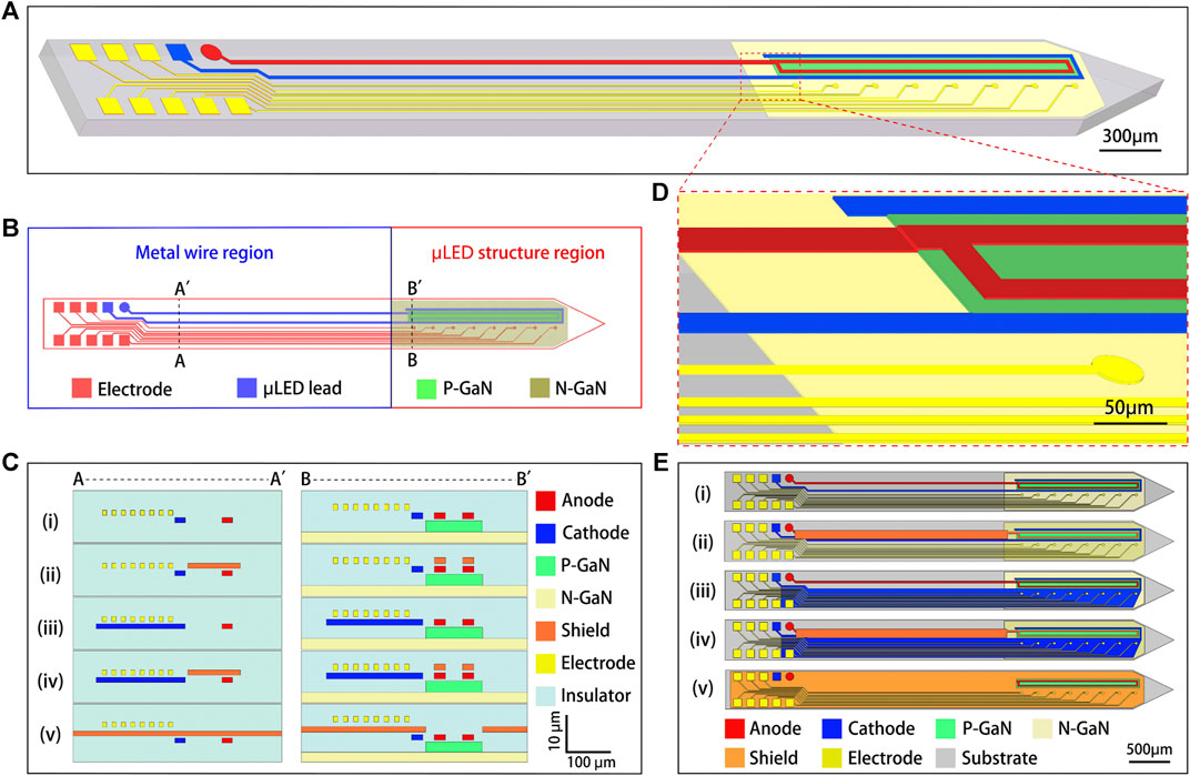
FIGURE 1. (A) The 3D simulation model of no-shielding optrode. (B) The divided region and selected modeling sections in optrode’s layout design. (C) The 2D simulation models of sections in (B) with different shielding schemes, (i) no shielding measure, (ii) adding shielding metal wire above the μLED’s anode metal (wiring-above-anode), (iii) widening the μLED’s cathode metal (widening-cathode), (iv) combining wiring-above-anode with widening-cathode (combined-shielding), (v) adding a whole shielding layer between the anode and cathode layer and the recording electrode layer (whole-shielding-layer). (D) The enlarged local structure of the 3D model in (A). (E) The top view of 3D simulation models with the same shielding schemes as (C).
The metal wire region mainly consists of the metal traces of the μLED and recording electrodes, in which the only interference source is the anode metal trace. The μLED structure region is the formation area of the PN junction. It includes the P-type and N-type gallium nitride (GaN) layer in addition to the metal traces. Since the GaN epitaxial wafers that we used have a structure with the P-type layer on the top and the N-type layer on the bottom, the P-type layer is also an interference source that cannot be ignored in the μLED structure region apart from the anode metal and the N-type layer mentioned in literature (Kim et al., 2016). Based on the interference source analysis, we constructed the 2D modeling of the metal wire region and the μLED structure region shown in Figure 1C. The wiring-above-anode is mainly designed to cope with the interference from anode wire, and the widening-cathode is for the N-GaN interference. The first three shielding methods are double-layer metal structures. There only needs to change the original metal layer shape, and no extra process flow is added. The last one is a three-layer metal structure, requiring an additional metal deposition process. The main difference between the models is that the P-GaN and N-GaN layers exist in the μLED structure region, resulting in that the shielding layer cannot cover the light-emitting area of the μLED.
We have also constructed 3D optrode models to reflect the electric field distribution more accurately in the 3D space. All the shielding schemes are the same as 2D modeling. The 3D model of no-shielding optrode is especially shown in Figure 1A, designed according to the actual device size (6,000 × 500 × 5 μm3). And the top view of other shielding schemes is shown in Figure 1E. The 3D modeling has both the characteristics of the metal wire region and the μLED structure region. A light window needs to be left above the light-emitting area in the shielding layer. All the electric field simulation models are set in an infinite air environment in order to simulate the real electric field distribution (Supplementary Figure S1).
In the electrical simulation, the potential is most commonly used to assess the magnitude of EMI according to the literature (Kim et al., 2016) (Ji et al., 2020; Kim et al., 2020). We did both static analyses (DC analysis) to observe the electrode potential when the μLED at the maximum input and transient analyses (time-domain analysis) to record the waveform reflecting the electrode potential varied with the μLED input voltage. In terms of material, the electrodes, leads, and shield are provided as metal, the rest of the shank is provided as insulator, and the shank is surrounded by air. These materials need to set the electrical conductivity (δ) and relative permittivity (ε), as shown in table 1.

TABLE 1. Electrical conductivity and relative permittivity configuration of different materials.
In the static simulation, a 3 V DC voltage is applied to the anode metal, and the N-type GaN layer was applied with 10 mV according to literature (Kim et al., 2016). Considering that the P-type layer is connected to the anode metal, we also assume it to be 3 V following the worst case. In the transient simulation, pulse signals are separately applied to the anode (3 V, 1 Hz), P-type GaN (3 V, 1 Hz), and N-type GaN (10 mV, 1 Hz). The cathode metal and the shielding layer are always grounded during all the simulations. The recording electrodes are set to be no current flowing in, assuming that the amplifier connected with the electrode is ideal. These models are calculated through FEM, and the meshing of a 3D model is shown in Figure 2A.
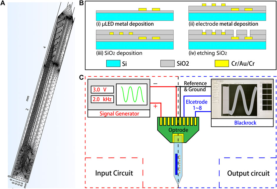
FIGURE 2. (A) 3D model meshing of no shielding optrode. (B) Partial process flow of the simplified optrode. (C) The in vitro system for testing the optrode shielding effect, consisting of a signal generator and a multi-channel recording system.
To verify the simulation results, we designed and manufactured simplified optrode devices with corresponding shielding methods for in vitro tests. Considering that electromagnetic interference is mainly involved in our research and the anode metal is the key interference source, whether the μLED is conductive can be ignored. So we designed simplified optrode devices to reduce the process complexity and shorten the verification time. Only the metal traces of the μLED and the recording electrodes are retained. There is no P-type and N-type GaN layer in the μLED structure region so that we can tape out on the silicon wafers grown with SiO2 rapidly. The simplified device can also exclude the influence of other noise sources in optrode, such as the noise-induced by the photovoltaic effect (Packer et al., 2013). We only fabricated the first four kinds of devices corresponding to the electrical field simulations, considering that the whole-shielding-layer scheme needs extra process steps which means higher cost, more difficult process and lower yield. Actually, the comparison of four kinds of devices is enough to illustrate our point of view.
The partial manufacturing process of the simplified optrode is shown in Figure 2B, and the detailed processes are as follows: 1) cleaning silicon wafers with silicon dioxide on the upper surface; 2) spinning coating photoresist (AZ4340) at 4,000 revolutions per second; transferring the patterns of μLED metal traces from the mask to the substrate by lithography; 3) metal deposition of Cr/Au/Cr with 5/100/5 nm thickness; 4) metal lift-off to get the patterned metal traces of the μLED; 5) depositing SiO2 with 100 nm thickness by PECVD; 6) repeating the above steps (2–5) to obtain the metal traces of the recording electrodes; 7) etching SiO2 to expose the electrode areas and the back-end pads. After all the processes are completed, we diced the wafer to release the optrode shank and welded the shank to the PCB by gold wire bonding, then applied UV glue to the welding area to complete the optrode package.
Based on the packaged optrode devices, we constructed the test system to verify the shielding effect (Figure 2C). Given that we usually care about the interference near the spike frequency, the signal generator is used to apply a sinusoidal voltage (3 V, 2 kHz) to the μLED’s metal traces. A multi-channel neuron data recording system (HTRP-128, Blackrock Microsystems, United States) is used to record the interference potential on the electrodes. The two instruments need to be connected to the same ground wire, and the entire test system requires a well-shielded environment. We have designed two kinds of interfaces to connect the optrode and the multi-channel recorder. One is used for all types of optrodes, and the other is designed for wiring-above-anode and whole-shielding-layer to make the shielding layer above the anode ungrounded. The test was carried out in the air. We selected three devices of each type to test the interference potential on the electrodes. The experimental and simulation results are analyzed from multiple perspectives, including logical analysis, circuit modeling, derivation of equations, and FEM.
The 2D electrostatic field simulation results are shown in Figure 3A, and the potential distribution on the 2D section is visually represented. Compared with no shielding measure, it can be clearly seen that no matter which shielding measure is adopted, the potential of the recording electrode area is significantly reduced in the metal wire region. We can also see that the whole-shielding-layer has the best shielding effect, the combined-shielding is the second, and the wiring-above-anode is the worst.
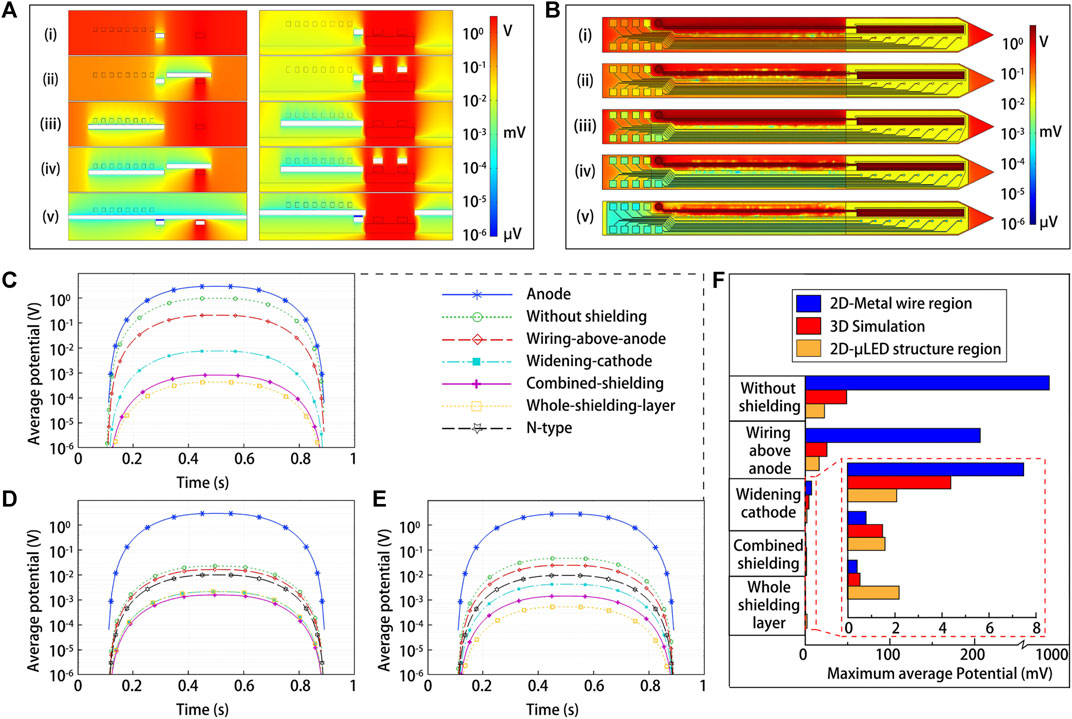
FIGURE 3. (A) The 2D potential distribution of the metal-wire region (left) and the μLED-structure region (right) in electrostatic field simulation. (B) The top view of 3D potential distribution results in electrostatic field simulation. (C–E) The time-domain curves of different shielding methods that reflect the eight electrode sites’ average potential over time in (C) metal wire region simulation, (D) μLED structure region simulation, and (E) 3D simulation. (F) The comparison of the maximum average potential between 2D and 3D time-domain simulation results.
While in the μLED structure region, the potential distribution results are much different from the metal wire region. First of all, a significantly lower potential distribution can be seen in the case of no shielding measure. We had assumed that the 10 mV voltage applied with the N-type layer is an interference source according to (Kim et al., 2016), but it is more like a shielding layer actually, pulling down the recording electrode potential. Secondly, the shielding effect of wiring-above-anode is extremely poor. It is designed for the μLED anode metal, and it does not have too much shielding effect on the N-type layer interference. What makes it worse is that the shielding layer cannot block the P-type interference. This also results in that the combined-shielding have a similar effect with the widening-cathode. Finally, the shielding effect of the whole-shielding-layer becomes worse. Due to the existence of the light-emitting area, the interference source below cannot be completely covered.
These differences can be observed from the time-domain simulation results more clearly, as shown in Figures 3C,D. In the time-domain analysis, a sine pulse signal of 1 Hz is inputted to the interference sources, represented with the blue line in Figures 3C–E for the anode and the black line in Figures 3D,E for the N-type layer. And then the recording electrodes potential which changes over time can be outputted in the software. Since there are eight electrodes in total, the average potential of these electrodes is used to represent the magnitude of interference. We can see that all the average potential changes with the excitation signal synchronously in both 2D simulation results. Furthermore, in the metal wire region, the effects of different shielding schemes are consistent with the electrostatic simulation results according to the numerical range of the average potential. The whole-shielding-layer has the lowest potential, the combined-shielding is slightly higher, and the wiring-above-anode is two orders of magnitude higher than them. While in the μLED structure region, the result is clearly different from the metal wire region, just as reflected in the electrostatic field simulation results. And it can be further seen that the combined-shielding has the best shielding effect, the widening-cathode and the whole-shielding-layer are almost the same, and the wiring-above-anode is the worst.
The huge differences in the 2D electric field simulation indicate that a single 2D simulation is not enough to represent the true spatial potential distribution in a non-uniform optrode device. Thus the 3D simulation is necessary. The 3D electrostatic field simulation results are shown in Figure 3B. It can be observed that the 3D potential distribution has both the characteristics of the metal wire region and the μLED structure region. For all the shielding measures, the shielding effect is the same order as the 2D metal wire region. While the electrode potential of no shielding measure is much lower, and the wiring-above-anode has little shielding effect, which is similar to the μLED structure region.
We can draw the same conclusions from the 3D time-domain result (Figure 3E). The wiring-above-anode is a little lower than no shielding measure in average potential, and they are close to the input voltage of the N-type layer. Although the average potential is consistent with the 2D metal wire region in order, it is different in the numerical range. This can be reflected in Figure 3F, in which we chose the peak value of the time-domain curves to compare the 2D and 3D results. We can further see that the 3D potential values are all between the metal wire region and the μLED structure region for each shielding measure. This is because the 3D simulation can be regarded as the synthesis of many 2D simulations, and it proves that the 3D simulation is more reasonable to be used in the optrode EMI analysis.
In the fabrication of the optrode, there are some important parameters that may influence the effect of the shielding layer. One is the process parameters, such as the thickness of the deposited metal layer and the center distance between the μLED metal layer and the electrode metal layer, which actually represents the thickness of the insulating layer between the two metal layers. The other is the layout design parameters, such as the width of the cathode, the width of the anode, and the edge-to-edge distance between the anode and the electrode region. Based on the 2D widening-cathode model, we have evaluated the impact of these parameters in detail and the result is shown in Figure 4.
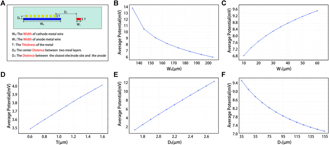
FIGURE 4. (A) The schematic diagram of various parameter definitions. (B–F) The relationship between the average potential of eight electrodes and (B) the width of cathode metal. (C) the width of anode metal. (D) the thickness of the metal layer. (E) the center distance between the μLED metal layer and the electrode metal layer. (F) the edge-to-edge distance between the anode and the electrode region.
In order to get a better shielding effect, the optrode needs to be designed with larger W0 and D1, smaller W1, T, and D0. But the precondition is to ensure the feasibility of the process, suitable device size, and stable device performance. Furthermore, we define the ratio of the average potential to these parameters as the significance to the shielding effect. We can see that D0 (its “significance” is about 10 mV/μm) should be given priority compared with T (0.5 mV/μm) between the two process parameters. Similarly, the W0 (110 μV/μm) is much more important than D1 (24 μV/μm) and W1 (56 μV/μm) during layout parameters.
A packaged optrode is shown in Figure 5A. We tested more than three times for each selected device, and the data recorded by the multi-channel system is averaged. The result is shown in Figure 5B. The recorded potential is reduced in the order of without shielding, wiring-above-anode, widening-cathode, and combined-shielding, proving the effectiveness of our designed shielding layers. We can also see the shielding effect by comparing the same optrode with different interfaces (Figure 5C). The average potential is obviously dropped after the shielding layer above the anode is grounded. There is no significant difference in potential values for the same type of device. Therefore, we averaged the values for each type and compared them with the 3D simulation result, as shown in Figure 5D. It is obvious that the variation trend of the experimental results is consistent with the simulation results under different shielding methods. This shows that the simulation results are effective for qualitative analysis. We can know whether the designed shielding methods are effective and which kind of shielding has a better effect through the simulation results.
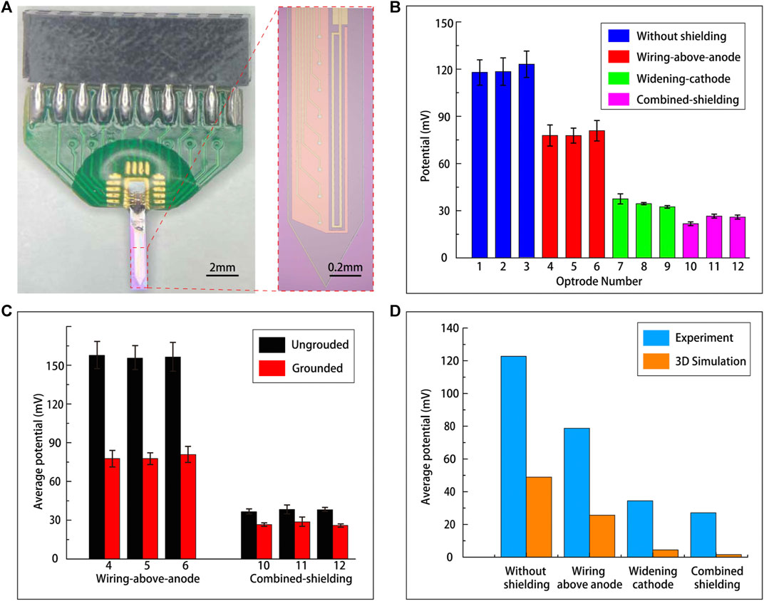
FIGURE 5. (A) The combined-shielding optrode packaged on PCB. (B) The shielding effect test results of four optrode types (three devices for each type and eight electrodes for each device). The error bar represents standard deviations (SD) and the horizontal axis is the number of the device. (C) The comparison of ungrounded and grounded shielding layer in wiring-above-anode and combined-shielding optrodes. The error bar represents standard deviations (SD) and the horizontal axis is the number of the device. (D) The comparison of experimental results and 3D simulation results under different shielding methods.
Although the experimental and simulation results have the same trend, they are not consistent in quantity. In order to explain this difference, we constructed different circuit models corresponding to the simulation environment and the actual test environment. And firstly we found that the electrode potential observed in the existing simulation model is not the real interference potential on the recording electrode but the spatial potential at the location where the recording electrode is. The spatial potential (Vr) is dependent on the distance from the interference source, as shown in Figure 6A. It is related to the amplitude of the noise source (Vs) but has nothing to do with the frequency, which is not in coincidence with reality. While the real electrode interference is a kind of coupled voltage due to the distributed capacitance between the recording electrode and the μLED anode, as shown in Figure 6B. The larger the equivalent capacitance (C1) is, the greater the coupled voltage (Vn) is. And it will become higher as the frequency (ω) increases. This relationship can be expressed as Eq. 1.
where Z can be replaced by Za (a coupling capacitor between the electrode and the ground) in the air, and can be replaced by Zp [a first-order R-C model of the electrode-electrolyte interface (Nathan and Jafari, 2015)] in the phosphate buffer saline (PBS). The shielding layer can just lower the Vn by reducing C1, which can be reduced to zero under ideal circumstances.
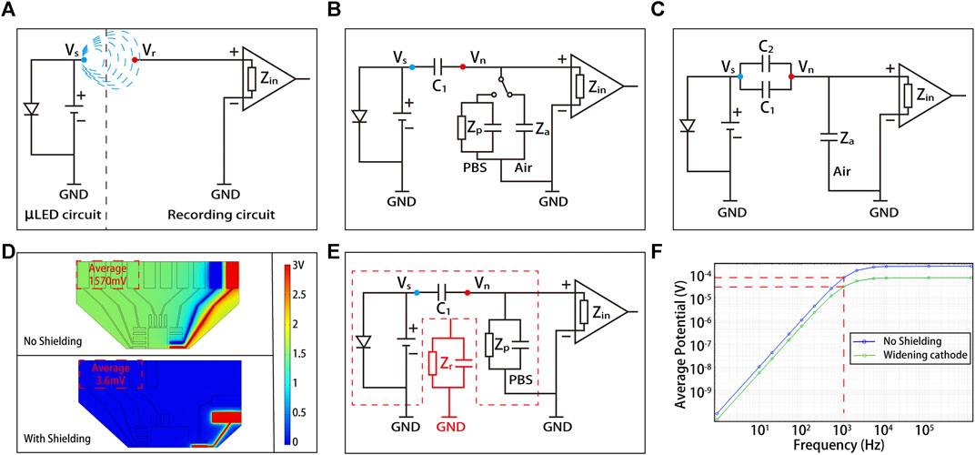
FIGURE 6. (A) The circuit model corresponding to the qualitative simulation environment. (B) The circuit model corresponding to the ideal test environment in air or PBS. (C) The circuit model corresponding to the actual test environment in air. (D) The simulation result of the new PCB’s shielding effect. (E) The circuit model corresponding to a quantitative simulation model used to analyze the electric field interference in optrode. (F) The comparison between no-shielding and widening-cathode using the quantitative simulation model for analysis.
The spatial potential and the coupled voltage are completely two different concepts. Under the same conditions, the former is much larger than the latter, which partly explains why the simulation result (whole-shielding with 550 μV is the best) in Figure 3 is much higher than the background noise (lower than 20 μV) of common neural recording systems. But there is a positive correlation between them. It is not difficult to understand that the higher the spatial potential is at a point, the greater the coupled voltage will be when a recording electrode is located there. To better illustrate this point, we studied the relationship between the width of cathode metal (W1), the width of anode shielding metal (W2), the spatial potential (U0), and the coupling capacitance (C0) which can represent the coupled voltage according to Eq. 1, based on the widening-cathode and the wiring-above-anode methods in 2D electric field simulation. It can be clearly seen from Figure 7 that there is a positive correlation between the spatial potential and the coupling capacitance. It means that when the shielding layer is widened, the spatial potential will decrease, and the coupling capacitance will become smaller, resulting in a lower coupled voltage. The result indicates that it is feasible to evaluate the effects of various shielding schemes by observing the spatial potential of the electrode area in software simulation, but it can only be qualitatively analyzed and cannot be quantified.
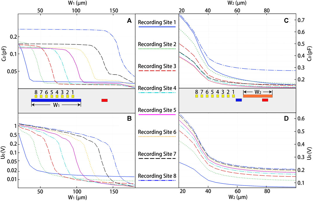
FIGURE 7. The relationship between (A) the coupling capacitance and the width of the cathode, (B) the spatial potential and the width of the cathode, (C) the coupling capacitance and the width of anode shielding metal, (D) the spatial potential and the width of anode shielding metal for eight recording electrodes.
Another factor that causes the difference between the experimental and the simulation results is the interference from the outside of the optrode shank, such as the welding pads at the stern, the PCB, and the interface with the amplifier. These interferences can be represented as a coupling capacitor (C2) in Figure 6C. The presence of C2 will result in an increase in Vn, and there will be a lower limit for reducing Vn by shielding layer, which indicates why the experiment result is so high in Figure 4D. The relationship can be expressed as Eq. 2.
And these interferences can be reduced by a more reasonable back-end package and interface design. For example, we have designed a new PCB with a whole-shielding layer that can reduce the interference by more than 400 times (Figure 6D).
From the above analysis, it is not difficult to see the shortcomings of the current simulation model, that is, only qualitative analysis can be performed. Thus we constructed a quantitative simulation model according to Figure 6E. Here we firstly connect the recording electrode to an R-C model using the software’s circuit function, where the resistance (R) and the capacitance (C) can be obtained by the electrochemical impedance test of the electrodes. And secondly, we have considered the PBS environment by which the optrode is surrounded. This kind of conductive solution is difficult to use specific material to represent in the software. But considering that the solution is connected to the ground through a reference electrode, we can also simplify it to be a grounded R-C model which is applied to the model boundary. What’s different is that the resistance (R) and the capacitance (C) should be obtained from the reference electrode impedance, which is much smaller than the recording electrode.
The new quantitative simulation model is used to analyze the electric field interference in no-shielding and widening-cathode optrode, and the frequency-domain simulation result is shown in Figure 6F. It can be seen that the electrode potential is higher with the frequency increases, which is consistent with reality. When it is at 1 kHz, the interference potential under no shielding is about 70 μV, which is the same order with the amplitude of a spike. With widening-cathode shielding, the potential is reduced to about 20 μV, enough to meet the actual needs if the model parameters are reasonable. In addition, the time-domain simulation result (Supplementary Figure S2) shows that noise spikes appear on the recording electrodes when the input signal is flipped, which is similar to the actual situation. It also demonstrates the shielding effect of widening-cathode method. These results only show the feasibility of quantitative analysis to electric field interference in optrode, but the specific parameters and components of the simulation model still need to be perfected and its reliability needs to be verified by actual test using the new designed device with a more reasonable package and connection.
We not only analyzed the EMI inside the optrode caused by electrical field, but also considered the possible interference caused by magnetic field. As the term EMI describes, the interference of the electric field and magnetic field often exists at the same time under the action of the varied excitation signal. The magnetic field simulation results (Supplementary Figure S3) show that the magnetic field interference is much smaller than the electrical field interference. This may be due to the small footprint of the optrode device. According to our coil model, the potential at the ends of the induction coil (Vout) is related to the maximum magnetic flux in the coil (Ф), and the magnetic flux is a function of the magnetic field strength (B) and the area enclosed by the induction coil (S), namely:
Considering that the magnetic field strength (B) is proportional to the current passing through the excitation coil (I), when the input voltage is constant, the magnetic field strength is inversely proportional to the resistance of the input circuit (R). Thus we can derive that when the device footprint is scaled down by L times, the resistance (R) will increase by L times, the area (S) will be reduced by L2 times, and the magnetic flux (Ф) will be reduced by L3 times. This means that the magnetic flux will drastically decrease as the device footprint shrinks. Therefore, the magnetic field interference can be ignored compared with the electric field interference for the small footprint optrode we designed.
In this paper, we evaluated four designed shielding schemes by in-depth and comprehensive electrical field simulations and discussed how to design the shielding layer with a better effect based on FEM. What is more, we fabricated corresponding simplified optrode devices and proved the simulation results to be reliable for quantitative analysis by in vitro experiments. We also explained the difference between the simulation results and the experimental results in quantity and provided feasible solutions. Finally, we performed a magnetic field simulation to show that the magnetic field interference is negligible in micro-sized optrodes. This research is very meaningful for understanding the EMI sources in optrode, guiding the shielding design, and fabricating low-noise optrode.
In the future, we plan to perfect the proposed quantitative simulation model, through which we can directly know whether the shielding effect can meet the actual needs. This will significantly reduce the cost of device manufacturing. Moreover, we will adopt the combined-shielding or the whole-shielding-layer in our optrode, then verify the designed shielding layer effect through animal experiments.
The original contributions presented in the study are included in the article/Supplementary Material, further inquiries can be directed to the corresponding author.
YaW is mainly responsible for the simulation work, experimental test and paper writing. YL helps design the device and participates in the introduction writing of this paper. XY guides the manufacturing process of the device. XW participates in the device test and helps revise the paper. YiW provides experimental equipment and helps build experimental test platforms. WP provides device manufacturing equipment and helps design experiments.
The project was supported by the National Key R&D Project of China (2017YFA0205903, 2017YFA0701100); National Natural Science Foundation of China (61634006, 61671424, 62071447); Strategic Priority Research Program of Chinese Academy of Science (XDB32030100, XDB32040200); Key research program of Frontier science, CAS, QYZDY-SSW-JSC004. CAS pilot project: XDA16020902; Beijing S&T planning task, Z161100002616019.
The authors declare that the research was conducted in the absence of any commercial or financial relationships that could be construed as a potential conflict of interest.
All claims expressed in this article are solely those of the authors and do not necessarily represent those of their affiliated organizations, or those of the publisher, the editors and the reviewers. Any product that may be evaluated in this article, or claim that may be made by its manufacturer, is not guaranteed or endorsed by the publisher.
We gratefully acknowledge the assistance of Shuo Chen and Huiping Tian for their guidance in writing this paper. We also thank Qiang Gui for guiding the process flow of the device manufacturing.
The Supplementary Material for this article can be found online at: https://www.frontiersin.org/articles/10.3389/fnano.2021.758484/full#supplementary-material
Adam, Y., Kim, J. J., Lou, S., Zhao, Y., Xie, M. E., Brinks, D., et al. (2019). Voltage Imaging and Optogenetics Reveal Behaviour-dependent Changes in Hippocampal Dynamics. Nature 569 (7756), 413–417. doi:10.1038/s41586-019-1166-7
Aldaoud, A., Soto-Breceda, A., Tong, W., Conductier, G., Tonta, M. A., Coleman, H. A., et al. (2018). Wireless Multichannel Optogenetic Stimulators Enabled by Narrow Bandwidth Resonant Tank Circuits. Sensors Actuators A: Phys. 271, 201–211. doi:10.1016/j.sna.2017.12.051
Fakhoury, M. (2021). Optogenetics: A Revolutionary Approach for the Study of Depression. Prog. Neuro-Psychopharmacology Biol. Psychiatry 106, 8. doi:10.1016/j.pnpbp.2020.110094
He Zhang, W. P., Yang, X., Guo, X., Xing, X., Gui, Q., and Chen, H. (2016). “A Sapphire Based Monolithic Integrated Optrode,” in 38th Annual International Conference of the IEEE.
Ji, B., Ge, C., Guo, Z., Wang, L., Wang, M., Xie, Z., et al. (2020). Flexible and Stretchable Opto-Electric Neural Interface for Low-Noise Electrocorticogram Recordings and Neuromodulation In Vivo. Biosens. Bioelectron. 153, 112009. doi:10.1016/j.bios.2020.112009
Kampasi, K., English, D. F., Seymour, J., Stark, E., McKenzie, S., Vöröslakos, M., et al. (2018). Dual Color Optogenetic Control of Neural Populations Using Low-Noise, Multishank Optoelectrodes. Microsyst Nanoeng 4, 16. doi:10.1038/s41378-018-0009-2
Khurram, A., and Seymour, J. P. (2013). “Investigation of the Photoelectrochemical Effect in Optoelectrodes and Potential Uses for Implantable Electrode Characterization,” in 2013 35th Annual International Conference of the Ieee Engineering in Medicine and Biology Society, New York (IEEE), 3032–3035. doi:10.1109/embc.2013.6610179
Kim, K., Vöröslakos, M., Seymour, J. P., Wise, K. D., Buzsáki, G., and Yoon, E. (2020). Artifact-free and High-Temporal-Resolution In Vivo Opto-Electrophysiology with microLED Optoelectrodes. Nat. Commun. 11 (1), 2063. doi:10.1038/s41467-020-15769-w
Kim, K., English, S., McKenzie, F., Wu, E., Stark, J., Seymour, P.-C., et al. (2016). “GaN-on-Si Mu LED Optoelectrodes for High-Spatiotemporal-Accuracy Optogenetics in Freely Behaving Animals,” in 2016 Ieee International Electron Devices Meeting (New York: IEEE).
Kim, T.-i., McCall, J. G., Jung, Y. H., Huang, X., Siuda, E. R., Li, Y., et al. (2013). Injectable, Cellular-Scale Optoelectronics with Applications for Wireless Optogenetics. Science 340 (6129), 211–216. doi:10.1126/science.1232437
Libbrecht, S., Hoffman, L., Welkenhuysen, M., Van den Haute, C., Baekelandt, V., Braeken, D., et al. (2018). Proximal and Distal Modulation of Neural Activity by Spatially Confined Optogenetic Activation with an Integrated High-Density Optoelectrode. J. Neurophysiol. 120 (1), 149–161. doi:10.1152/jn.00888.2017
Montgomery, K. L., Yeh, A. J., Ho, J. S., Tsao, V., Mohan Iyer, S., Grosenick, L., et al. (2015). Wirelessly Powered, Fully Internal Optogenetics for Brain, Spinal and Peripheral Circuits in Mice. Nat. Methods 12 (10), 969–974. doi:10.1038/nmeth.3536
Nathan, V., and Jafari, R. (2015). Design Principles and Dynamic Front End Reconfiguration for Low Noise EEG Acquisition with Finger Based Dry Electrodes. IEEE Trans. Biomed. Circuits Syst. 9 (5), 631–640. doi:10.1109/tbcas.2015.2471080
Packer, A. M., Roska, B., and Häusser, M. (2013). Targeting Neurons and Photons for Optogenetics. Nat. Neurosci. 16 (7), 805–815. doi:10.1038/nn.3427
Park, S. I., Shin, G., McCall, J. G., Al-Hasani, R., Norris, A., Xia, L., et al. (2016). Stretchable Multichannel Antennas in Soft Wireless Optoelectronic Implants for Optogenetics. Proc. Natl. Acad. Sci. USA 113 (50), E8169–E8177. doi:10.1073/pnas.1611769113
Qazi, R., Kim, C. Y., Byun, S.-H., and Jeong, J.-W. (2018). Microscale Inorganic LED Based Wireless Neural Systems for Chronic In Vivo Optogenetics. Front. Neurosci. 12, 764. doi:10.3389/fnins.2018.00764
Reddy, J. W., Kimukin, I., Stewart, L. T., Ahmed, Z., Barth, A. L., Towe, E., et al. (2019). High Density, Double-Sided, Flexible Optoelectronic Neural Probes with Embedded μLEDs. Front. Neurosci. 13, 745. doi:10.3389/fnins.2019.00745
Segev, E., Reimer, J., Moreaux, L. C., Fowler, T. M., Chi, D., Sacher, W. D., et al. (2017). Patterned Photostimulation via Visible-Wavelength Photonic Probes for Deep Brain Optogenetics. Neurophotonics 4 (1), 011002. doi:10.1117/1.NPh.4.1.011002
Sha, Y., Lin, C., Xie, H., Yi, X., Zhan, T., Liu, C., et al. (2021). Implantable Wirelessly Powered Optoelectronic Device for Optogenetics. Opt. Eng. 60 (2), 10. doi:10.1117/1.oe.60.2.027101
Shin, H., Son, Y., Chae, U., Kim, J., Choi, N., Lee, H. J., et al. (2019). Multifunctional Multi-Shank Neural Probe for Investigating and Modulating Long-Range Neural Circuits In Vivo. Nat. Commun. 10 (1), 3777. doi:10.1038/s41467-019-11628-5
Wang, L. C., Wang, M. H., Ge, C. F., Ji, B. W., Guo, Z. J., Wang, X. L., et al. (2019). The Use of a Double-Layer Platinum Black-Conducting Polymer Coating for Improvement of Neural Recording and Mitigation of Photoelectric Artifact. Biosens. Bioelectron. 145, 111661. doi:10.1016/j.bios.2019.111661
Wu, F., Stark, E., Im, M., Cho, I.-J., Yoon, E.-S., Buzsáki, G., et al. (2013). An Implantable Neural Probe with Monolithically Integrated Dielectric Waveguide and Recording Electrodes for Optogenetics Applications. J. Neural Eng. 10 (5), 056012. doi:10.1088/1741-2560/10/5/056012
Keywords: μLED optrode, electromagnetic interference, electromagnetic shielding, optogenetics, finite element method
Citation: Wang Y, Li Y, Yang X, Wu X, Wang Y and Pei W (2021) Analysis of Electromagnetic Interference and Shielding in the μLED Optrode Based on Finite Element Method. Front. Nanotechnol. 3:758484. doi: 10.3389/fnano.2021.758484
Received: 14 August 2021; Accepted: 15 November 2021;
Published: 02 December 2021.
Edited by:
Xing Sheng, Tsinghua University, ChinaReviewed by:
Xiaojie Duan, Peking University, ChinaCopyright © 2021 Wang, Li, Yang, Wu, Wang and Pei. This is an open-access article distributed under the terms of the Creative Commons Attribution License (CC BY). The use, distribution or reproduction in other forums is permitted, provided the original author(s) and the copyright owner(s) are credited and that the original publication in this journal is cited, in accordance with accepted academic practice. No use, distribution or reproduction is permitted which does not comply with these terms.
*Correspondence: Weihua Pei, cGVpd2hAc2VtaS5hYy5jbg==
Disclaimer: All claims expressed in this article are solely those of the authors and do not necessarily represent those of their affiliated organizations, or those of the publisher, the editors and the reviewers. Any product that may be evaluated in this article or claim that may be made by its manufacturer is not guaranteed or endorsed by the publisher.
Research integrity at Frontiers
Learn more about the work of our research integrity team to safeguard the quality of each article we publish.