 Yajing Wang1
 Lin Peng
94% of researchers rate our articles as excellent or good
Learn more about the work of our research integrity team to safeguard the quality of each article we publish.
Find out more
ORIGINAL RESEARCH article
Front. Nanotechnol., 15 March 2021
Sec. Nanocatalysis
Volume 3 - 2021 | https://doi.org/10.3389/fnano.2021.627387
Using the first principle method we studied, theoretically and in detail, the structural, optical, and electronic properties of a charge-ordered indium halide perovskite Cs2In(I)In(III)Cl6 at high pressure. In this structure, In1, In2, and In3 are octahedrally coordinated, whereas In4 is at the center of a pentagonal bipyramid. The charge of In on In1 and In2 sites can be assigned to 3+, while In+ occupies In3 and In4 sites. The results indicated that the band gap decreases, and the electron excitation produces the red-shift of peak value of optical absorption coefficient in visible and infrared regions with increasing pressure, and the reflectivity decreases in visible and infrared regions with increasing pressure. These theoretical results provide a basis for designing related inorganic halide perovskites.
Halide perovskites with various compositions, dimensionalities, and morphologies, have been greatly developed over the last decade. The class of materials have a wide range of potential applications, such as photovoltaics, light-emitting diodes, photodetectors, and lasers, due to their remarkable optoelectronic properties (Dreizler and Gross, 1990; Retuerto et al., 2013; Yin and Kotliar, 2013; Filip et al., 2014; Amgar et al., 2016; He et al., 2017; Kovalenko et al., 2017; Vargas et al., 2017; Volonakis et al., 2017; Zhao et al., 2017; Han et al., 2018; Jeong et al., 2018; Lin et al., 2018; Lin et al., 2019a; Lin et al., 2019b; Tan et al., 2019; Chen et al., 2020; Li et al., 2020). Halide perovskites have the general formula ABX3 (Lin et al., 2019a), and the crystal symmetry and phase stability can be determined using the Goldschmidt’s tolerance factor t (Zhao et al., 2017). In the perovskite structure, a site can be occupied by either an inorganic ion (e.g., Cs+, Rb+, K+) or an organic ion [e.g., CH3NH3+ (MA+), HC(NH2)2+ (FA+)]; B is a divalent metal cation (e.g., Pb2+, Sn2+, or Ge2+) and X is a halide anion (e.g., I−, Br−, Cl−). The B cation has six nearest-neighbored anions X, and the A cation occupies a vacancy formed by eight corner-sharing [BX6]4− octahedrons (Lin et al., 2019a). Among the perovskite-type structure materials, the charge ordered materials Cs2B+B3+X6, such as Cs2Au+Au3+X6, and Cs2Tl+Tl3+X6 (X = Cl, Br, I), show unique properties, including potential high-Tc superconducting behaviors and semiconductor-metal transition at high pressures (Yin and Kotliar, 2013; Lin et al., 2019). For example, Cs2Tl+Tl3+Cl6 and Cs2Tl+Tl3+F6 perovskites were theoretically predicted to be potential superconductors if they were optimally doped and indicated high-Tc ∼20 and ∼30 K superconductivity under reasonably high pressures (Yin and Kotliar, 2013). These two compounds, together with a complete characterization of the samples were synthesized (Retuerto et al., 2013). Cs2Tl+Tl3+Cl6 is obtained as orange crystals in two different polymorphs: a tetragonal (I4/m) and a cubic (Fm-3m) phase. Cs2Tl+Tl3+F6 is formed as a light brown powder, also as a double cubic perovskite (Fm-3m). In all three Cs2Tl+Tl3+X6 phases, Tl+ and Tl3+ were located in two different crystallographic positions that accommodate their different bond lengths. Recently, polycrystalline samples of Cs1.17In0.81Cl3 were prepared by annealing a mixture of CsCl, InCl, and InCl3, stoichiometric for the targeted CsInCl3 (Tan et al., 2019). The composition Cs1.17In0.81Cl3 with both corner-sharing and edge-sharing InCl6 octahedra and InCl7 pentagonal bipyramids, is isostructural with tetragonal Cs2Tl+Tl3+Cl6 (I4/m). Subsequently, the In+/In3+-based charge-ordered halide perovskite compound Cs2In+In3+Cl6 [Cs2In(I)In(III)Cl6] has also been successfully synthesized through a solid-state reaction method, which shows a semiconductor-to-metal phase transition under high pressures (Lin et al., 2019a).
Despite the tremendous progress which has been made, challenges still remain with perovskites, which call for a better understanding of the fundamental mechanisms of halide. Pressure, a thermodynamic variable, provides a powerful tool to tune structures and properties (Li et al., 2020). On one hand, in combination with in situ characterization methods, high-pressure research could experimentally provide a better fundamental understanding. On the other hand, the properties of materials could be theoretically predicated at high pressure. In this work we shall discuss, theoretically and in detail, the structural, optical, and electronic properties of Cs2In(I)In(III)Cl6 at high pressure.
In this study, all structure optimizations are calculated by the generalized gradient approximation (GGA) with density functional theory (DFT) (Dreizler and Gross, 1990). The Perdew–Burke–Ernzerhof (PBE) functional is applied to describe the electron exchange correlation. At the present calculations, energy cutoff of plane-wave was set to be 400 eV, the special points sampling integration over the Brillouin zone were performed using a k-mesh of dimensions 4×4×4 k-points mesh according to a Monkhorst-Pack scheme. Geometrical optimization was conducted using the convergence of thresholds of 5 × 10⁻⁶ eV/atom for the total energy, all forces on atoms were converged to less than 0.01 eV/Å. The crystal structures have been energy-optimized by the above calculation method.
The linear optical properties for Cs2In(I)In(III)Cl6 can be obtained from the frequency-dependent complex dielectric function
Similarly, extinction coefficient is denoted by
General formula of reflectivity to find the reflection from surface of any material is given as
In the same way, absorption coefficient
The calculations were conducted on the Cs2In(I)In(III)Cl6 version of the structural model as shown in Figure 1, that is, without considering the apparent presence of Cs in the In sites or attendant vacancies in the crystal structure of Cs2In(I)In(III)Cl6. The crystallographic data of Cs2In(I)In(III)Cl6, according to the structural model described in Table 1. The structure of the Cs2In(I)In(III)Cl6 sample is very similar to that of CsTlCl3 (Retuerto et al., 2013). In this structure, there are two Cs sites, four In sites, and seven Cl sites. In1, In2, and In3 are octahedrally coordinated, whereas In4 is at the center of a pentagonal bipyramid. The charge of In on In1 and In2 sites can be assigned to 3+. The remaining two nominal In sites indicate a lower oxidation state on In3 and In4 sites. One would conclude that In+ occupies In3 and In4 sites.
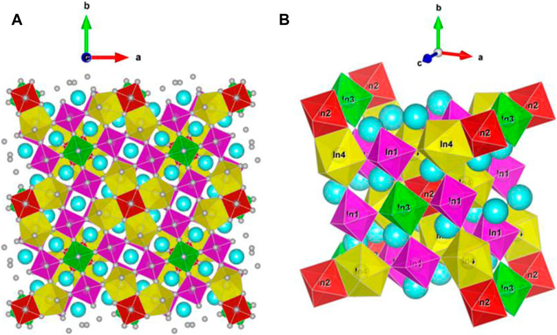
FIGURE 1. (Color online) Crystal structure of Cs2In(I)In(III)Cl6 with the space group I4/m (A) super cell (2 × 2 × 2), (B) conventional unit cell. Color code: In1 = magenta, In2 = red, In3 = green, In4 = orange, Cs = blue, and Cl = gray.
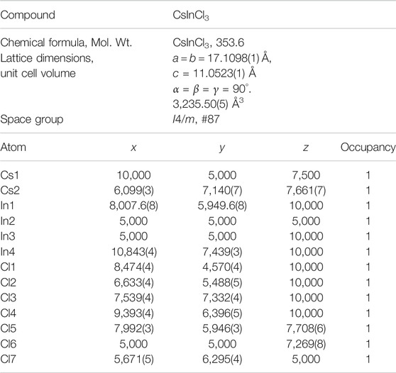
TABLE 1. Crystallographic data of CsInCl3, according to the structural model described in the text [Fractional Atomic Coordinates (× 104)].
Figure 2 represents electronic band structures of Cs2In(I)In(III)Cl6 under different pressures. It has been observed that under ambient conditions, the top of the valence band (VB) and bottom of the conduction band (CB) are located at X and N symmetry points, respectively, and the band-gap Eg calculated under ambient pressure is 2.02 eV (Figure 2A). Hence, Cs2In(I)In(III)Cl6 is regarded as an indirect band-gap semiconductor. Interestingly, while increasing the pressure, shifting the top of VB at P symmetry points toward the Fermi level was observed. Contrary to this, other symmetry points were observed to move away from the Fermi level. With the increasing pressure, the band-gap decreases and becomes zero at ∼27.5 GP, as shown in Figure 2F, which indicates the semiconductor-metal transition with the increasing pressures. The lattice constant a (a = b) ranges from 17.5779 Å (ambient pressure) to 14.5797 Å (32 GPa), and c ranges from 11.3175 to 9.5625 Å (Figure 2G). It is well known that GGA functional underestimates in calculating the electronic band-gap, but the use of hybrid exchange-correlation functionals, such as HSE06 and mBJ, provides better results (Tan et al., 2019). In addition, the calculated band gap here is much larger than the literature report (<1 eV) of theoretical CsInCl3 (Körbel et al., 2016). This is possibly attributed to the calculations carried out based on the experimental crystal structure. Meanwhile, we observe the semiconductor-metal transition appears at ∼27.5 GPa in our theoretical result, which is larger than experimental result (∼22 GPa) (Lin et al., 2019a). This could be attributed to the removal of some disorder components in our model, compared with the crystal structure shown in the Reference Lin et al. (2019a). The large indirect band gap suggests that this nonstoichiometric perovskite-derived phase is not a good candidate for photovoltaic application. These theoretical and experimental results, however, provide a basis for designing related inorganic halide perovskites for potential photovoltaic functions or superconductivity.

FIGURE 2. (Color online) Band structure and lattice constants at different pressure for Cs2In(I)In(III)Cl6(A) 0 GPa, (B) 3 GPa (C) 9 GPa, (D) 22 GPa (E) 32 GPa, (F) variation of band gaps at different pressures, and (G) variation of lattice constants at different pressures.
To further reveal the factors controlling the bandgap trends, density of states (DOS) and partial density of states (PDOS) based on variable control approaches were carried out. Firstly, to study the effect of In cations on bandgap trend, DOS and PDOS of Cs2In(I)In(III)Cl6 were calculated at 0 GPa, and shown in Figure 3. The calculation results indicated that In on In2 and In3 sites do not contribute to the basic electronic structures. The valence band maximum (VBM) is derived from the p orbitals of In on In4 sites and p orbitals of Cl, and their overlapping indicates the significant hybridization. The s orbitals of In on In1 sites, p orbitals of In on In4 sites and p orbitals of Cl constitute the conduction band minimum (CBM). The trend of difference value between VBM and CBM for Cs2In(I)In(III)Cl6 is consistent with the change of calculated bandgaps. With the increase in pressure from 0 to 27.5 GPa, the s and p orbitals of In on In1 sites, and the s and p orbitals of In on In4 sites lowered the bottom of conduction band (see Figure 4), and the metal–insulator transition occurs in the Cs2In(I)In(III)Cl6.
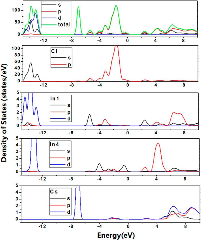
FIGURE 3. (Color online) Density of states and Partial density of states for Cs2In(I)In(III)Cl6 at 0 GPa pressure. The data for y-axis indicates the density of States (electrons/eV), and the data for x-axis indicates the photon energy (eV).
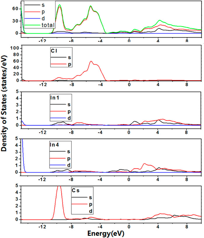
FIGURE 4. (Color online) Density of states and Partial density of states for Cs2In(I)In(III)Cl6 at 27.5 GPa pressure. The data for y-axis indicates the density of States (electrons/eV), and the data for x-axis indicates the photon energy (eV).
The real and imaginary parts of dielectric function for Cs2In(I)In(III)Cl6are shown in Figure 5. The complex dielectric function

FIGURE 5. (Color online) Dielectric function of Cs2In(I)In(III)Cl6 at different pressures.
The absorption coefficient determines the solar energy conversion efficiency and it indicates how far light of a specific energy (frequency) can penetrate into the material before absorption. With increasing pressure, the peak value of the absorption coefficient increases in visible and infrared regions as shown in Figure 6A. The electron excitation produces the red-shift of the peak value of the optical absorption coefficient. The reflectivity spectrum as a function of photon energy is shown in Figure 6B. We have observed that the reflectivity decreases with increasing pressure in visible and infrared regions.
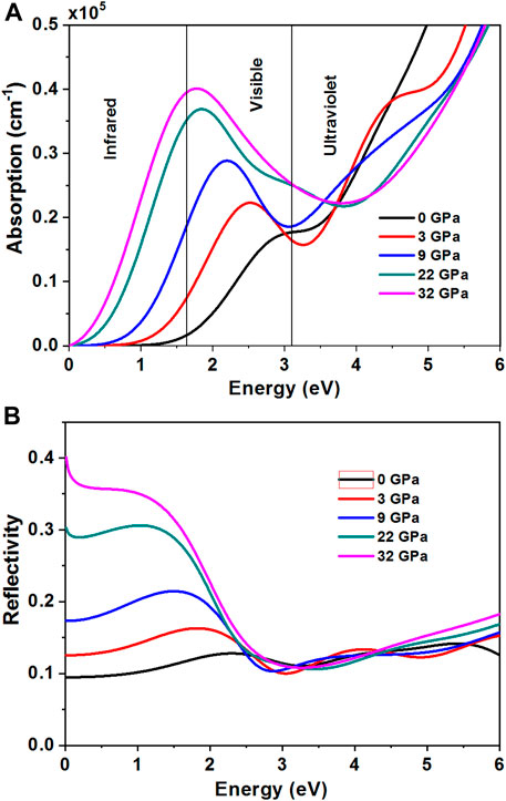
FIGURE 6. (Color online) Absorption coefficient and reflectivity of Cs2In(I)In(III)Cl6 at different pressures (A) Absorption coefficient, (B) Reflectivity.
In conclusion, using the first principle method, we studied theoretically and in detail the structural, optical, and electronic properties of a charge-ordered indium halide perovskite Cs2In(I)In(III)Cl6 at high pressure, based on the experimental crystal structure. With increasing pressure, the band gap of Cs2In(I)In(III)Cl6 decreases, which shows a semiconductor-to-metal phase transition under high pressures 27.5 GPa. The theoretical result is larger than the experimental result (∼22 GPa) due to the removal of disorder in the model. The peak value of optical absorption coefficient produces red-shift, and the reflectivity decreases in visible and infrared regions with increasing pressure. Meanwhile, the results show that high-pressure research provides a powerful tool to tune structures and properties. Thus, the properties of materials could be better understood by the method.
The raw data supporting the conclusions of this article will be made available by the authors, without undue reservation.
LP proposed the research idea and analysis; YW and SY performed theoretical calculations and manuscript; All authors reviewed the manuscript, have given approval to the final version of the manuscript, and confirmed the authorship to this work.
This work is sponsored by the National Natural Science Foundation of China (61875119), Shanghai Rising-Star Program (Grant No. 19QA1404000) and the Natural Science Foundation of Shanghai (No. 17ZR1411400).
The authors declare that the research was conducted in the absence of any commercial or financial relationships that could be construed as a potential conflict of interest.
Amgar, D., Aharon, S., and Etgar, L. (2016). Inorganic and hybrid organo‐metal perovskite nanostructures: synthesis, properties, and applications. Adv. Funct. Mater. 26, 8576–8593. doi:10.1002/adfm.201603752
Chen, S., Zhang, T., Liu, X., Qiao, J., Peng, L., Wang, J., et al. (2020). Lattice reconstruction of La-incorporated CsPbI2 Br with suppressed phase transition for air-processed all-inorganic perovskite solar cells. J. Mater. Chem. 8, 3351–3358. doi:10.1039/c9tc05736f
Filip, M. R., Eperon, G. E., Snaith, H. J., and Giustino, F. (2014). Steric engineering of metal-halide perovskites with tunable optical band gaps. Nat. Commun. 5, 5757. doi:10.1038/ncomms6757
Han, J. S., Le, Q. V., Choi, J., Hong, K., Moon, C. W., Kim, T. L., et al. (2018). Lead-free all-inorganic cesium tin iodide perovskite for filamentary and interface-type resistive switching toward environment-friendly and temperature-tolerant nonvolatile memories. ACS Appl. Mater. Interf. 28, 1705783. doi:10.1002/adfm.201705783
He, X., Liu, P., Zhang, H., Liao, Q., and Yao, J. (2017). Patterning multicolored microdisk laser arrays of cesium lead halide perovskite. Adv. Mater. 29, 1604510. doi:10.1002/adma.201604510
Jeong, B., Han, H., Choi, Y. J., Cho, S. H., Kim, E. H., Lee, S. W., et al. (2018). Polymer-assisted nanoimprinting for environment-and phase-stable perovskite nanopatterns. Adv. Funct. Mater. 28, 1706401. doi:10.1002/adfm.201706401
Körbel, S., Marques, M. A. L., and Botti, S. J. (2016). Stability and electronic properties of new inorganic perovskites from high-throughput ab initio calculations. J. Mater. Chem. C 4, 3157–3167. doi:10.1039/c5tc04172d
Kovalenko, M. V., Protesescu, L., and Bodnarchuk, M. I. (2017). Properties and potential optoelectronic applications of lead halide perovskite nanocrystals. Science 358, 745–750. doi:10.1126/science.aam7093
Li, M., Liu, T., Wang, Y., Yang, W., and Lü, X., (2020). Pressure responses of halide perovskites with various compositions, dimensionalities, and morphologies. Matter Radiat. Extremes 5, 018201. doi:10.1063/1.5133653
Lin, J., Chen, H., Gao, Y., and Cai, Y. (2019a). ,Pressure-induced semiconductor-to-metal phase transition of a charge-ordered indium halide perovskite. Proc. Natl. Acad. Sci. 116 (47), 23404–23409. doi:10.1073/pnas.1907576116
Lin, J., Chen, H., and Kang, J. (2019b). Copper (I)-based highly emissive all-inorganic rare-earth halide clusters. Matter 1, 180–191. doi:10.1016/j.matt.2019.05.027
Lin, J., Lai, M., and Dou, L. (2018). Thermochromic halide perovskite solar cells. Nat. Mater. 17, 261–267. doi:10.1038/s41563-017-0006-0
Retuerto, M., Emge, T., Hadermann, J., Stephens, P. W., and Li, M. R. (2013). Synthesis and properties of charge-ordered thallium halide perovskites, CsTl+ 0.5 Tl3+ 0.5 X3 (X= F or Cl): theoretical precursors for superconductivity? Chem. Mater. 25, 4071–4079. doi:10.1021/cm402423x
Tan, X., Stephens, P., and Hendrickx, M. (2019). Tetragonal Cs1. 17In0. 81Cl3: a charge-ordered indium halide perovskite derivative. Chem. Mater. 31, 1981–1989. doi:10.1021/acs.chemmater.8b04771
Vargas, B., Ramos, E., Perez-Gutierrez, E., Alonso, J. C., and Solis-Ibarra, D. J. (2017). A direct bandgap copper–antimony halide perovskite. J. Am. Chem. Soc. 139, 9116–9119. doi:10.1021/jacs.7b04119
Volonakis, G., Haghighirad, A. A., Milot, R. L., Sio, W. H., Filip, M. R., Wenger, B., et al. (2017). Cs2InAgCl6: a new lead-free halide double perovskite with direct band gap. J. Phys. Chem. Lett. 8, 772–778. doi:10.1021/acs.jpclett.6b02682
Yin, Z. P., and Kotliar, G. (2013). Rational material design of mixed-valent high-Tc superconductors. Europhys. Lett. 101, 27002. doi:10.1209/0295-5075/101/27002
Keywords: halide perovskites, band structure, charge-ordered indium, optic-electronic properties, high pressure
Citation: Wang Y, Yao S, Liu X, Chen G and Peng L (2021) First-Principles Study on Optic-Electronic Properties of Charge-Ordered Indium Halide Perovskite Cs2In(I)In(III)Cl6 at High Pressure. Front. Nanotechnol. 3:627387. doi: 10.3389/fnano.2021.627387
Received: 09 November 2020; Accepted: 01 February 2021;
Published: 15 March 2021.
Edited by:
Yi Yu, ShanghaiTech University, ChinaReviewed by:
Xun Zhangxun, ShanghaiTech University, ChinaCopyright © 2021 Wang, Yao, Liu, Chen and Peng. This is an open-access article distributed under the terms of the Creative Commons Attribution License (CC BY). The use, distribution or reproduction in other forums is permitted, provided the original author(s) and the copyright owner(s) are credited and that the original publication in this journal is cited, in accordance with accepted academic practice. No use, distribution or reproduction is permitted which does not comply with these terms.
*Correspondence: Lin Peng, cGxwZW5nQHNoaWVwLmVkdS5jbg==
Disclaimer: All claims expressed in this article are solely those of the authors and do not necessarily represent those of their affiliated organizations, or those of the publisher, the editors and the reviewers. Any product that may be evaluated in this article or claim that may be made by its manufacturer is not guaranteed or endorsed by the publisher.
Research integrity at Frontiers
Learn more about the work of our research integrity team to safeguard the quality of each article we publish.