 Yuege Zhou1,2
 Qingsheng Liu
- 1Beijing Key Laboratory of Environment and Reliability Test Technology for Aerospace Mechanical and Electrical Products, Beijing, China
- 2Beijing Institute of Spacecraft Environment Engineering, Beijing, China
- 3School of Reliability and Systems Engineering, Beihang University, Beijing, China
2.5D package realizes the interconnection of multiple dies through Si interposers, which can greatly improve the data transmission rate between dies. However, its multi-layer structure and high package density also place higher reliability requirements on the interconnection structure. As a key structure for interconnection, copper pillar bump (CPB) has small size, high heat generation, and thermal mismatch with silicon chips. The thermal fatigue failure of CPB has gradually become the main failure mode in 2.5D package. Due to the small size of CPB and the large proportion of intermetallic compound (IMC) layers, the lifetime prediction method of spherical solder joints is no longer suitable for CPB. Therefore, it is necessary to establish a fatigue lifetime prediction method for CPB. This paper establishes a method for obtaining the lifetime of CPB based on the basic theory of fatigue crack propagation. Using the extended finite element simulation method, the crack propagation lifetime of CPB under thermal cycling was obtained, and the influence of different IMC layer thickness on the fatigue lifetime of CPB was analyzed. The results indicated that the fatigue lifetime of cracks propagating in the IMC layer is lower than that of cracks propagating in the solder layer, and an increase in the thickness of the IMC layer leads to a significant decrease in the fatigue lifetime of CPB. The lifetime prediction method for CPB proposed in this paper can be used for reliability evaluation of 2.5D package, and has certain reference value for the study of the lifetime of CPB.
1 Introduction
With the increasing demand for product miniaturization, high I/O density, and heterogeneous integration, higher requirements have been put forward for the front end and back end processes of semiconductors. But currently, the process of transistors is approaching the physical limit, and the benefits of relying on reducing semiconductor gate width to increase integration are decreasing (Wong, 2021; Watanabe, 2009). Therefore, more and more manufacturers are shifting the direction of improving integration and reducing chip size from front end processes to back end processes, hoping to break through the physical size limitations of chips with more advanced packaging forms. Among them, the 2.5D package can package multiple chips with different functions and structures onto a Si interposers, achieving heterogeneous integration (Lancaster and Keswani, 2018; Zhang et al., 2021; Dale et al., 2020). Due to the shorter distance between chips, this package structure occupies less space, and it has lower power consumption and better electrical performance compared to traditional package (Liu et al., 2016).
In order to realize the vertical electrical connection of 2.5D package, various bump interconnection technologies are used, mainly including copper pillar bumps (CPBs) and C4 bumps (Liu et al., 2016; Zhang et al., 2015). Among these bump technologies, CPBs are the interconnect bumps with the smallest geometric size, shortest pitch, and highest density. Compared with traditional spherical bumps, cylindrical CPBs have higher aspect ratio and can solve the ultra-fine pitch problem of high-density package. At the same time, the CPBs also have excellent electrical and thermal conductivity properties, and the lead-free solder cap can also meet the ROHS requirements. Therefore, CPB technology is more and more widely used in various types of 2.5D and 3D package, and has gradually become a key link in the package.
However, as the size of CPB continues to decrease, the operating current continues to increase, and the working environment temperature is also getting higher, which leads to some problems in the application of 2.5D package. Due to the harmful effects of Pb-containing solders on the environment and human health, Pb-free materials such as SAC305 have been widely used as substitutes for interconnect materials under the National Electronics Manufacturing Initiative (Long et al., 2023). The solder cap material for CPB generally uses lead-free solder materials such as Sn-Ag or Sn-Ag-Cu. The solder joint is prone to producing rich intermetallic compounds (IMC) during use. Under long-term high-temperature action, the solder cap may even completely transform into an IMC layer (Rao et al., 2016; Na et al., 2022; Koo et al., 2007). With the emergence of the IMC layer, the mechanical strength and fracture toughness of the solder joints will decrease, causing crack in the welding helmet to expand more easily and reducing its fatigue lifetime (Gong et al., 2024). In addition, the 2.5D package has a high density and a large heat generation of the chip. The difference in thermal expansion coefficient between the copper pillar in CPB and the silicon material is significant, resulting in a serious thermal mismatch problem in this structure. As its size decreases, the failure of the CPB has become one of the main failure modes of 2.5D package (Jing et al., 2014). Therefore, studying the fatigue failure of CPB plays an important role in improving the reliability of 2.5D package.
Some authors have already noticed that the presence of IMC layers can affect the mechanical properties and reliability of CPB. Kwon et al. (2016) found that under thermal cycling conditions, an IMC layer is formed at the interface between solder and copper, and the thickness of the IMC layer also increases with time and temperature. When the z-direction stress caused by thermal expansion acts on the interface, the crack would propagate along the depletion zone, and eventually microcrack failure would occur. Ajay Kumar and Dutta (2018) analyzed the growth kinetics and shear deformation tests of IMC in thin Sn-3Ag-0.5Cu joints, and inferred that the increase in IMC content caused by heat treatment would lead to a deterioration of the mechanical properties of the joint due to the presence of initial microcracks. Zhu et al. (2020) conducted shear fatigue tests on CPB with different thicknesses of IMC layers and found that their fracture toughness decreased with increasing IMC thickness. They also applied the Coffin-Manon model to predict the fatigue lifetime of CPB, but the accuracy was slightly poor. Li et al. (2020) found that there are two locations for crack propagation at CPB, namely, Sn-Ag solder joint and IMC bump. They also compared the lifetime prediction results of the Darveaux model and Schubert model, and found that the latter should be more suitable for CPB, but both have significant deviations.
At present, many research has been conducted on traditional spherical solder joints. Based on different theoretical systems, lifetime prediction models suitable for different types of solder joints have been proposed. But among these models, most only consider the constitutive model of solder (Su et al., 2019). Generally speaking, in current 2.5D package, the diameter of the more commonly used CPB is about 30 μm, the diameter of the C4 solder ball is about 100 μm, and the diameter of the BGA solder ball is several hundred microns. The volume of C4 solder joints and BGA solder joints is hundreds or thousands of times that of CPB. The proportion of the IMC layer in CPB is much larger than that in BGA solder joints (Yu et al., 2024; Chen et al., 2022). The impact of the IMC layer on the thermal fatigue of CPB cannot be ignored. If the previous lifetime prediction model is completely applied, it may lead to significant prediction deviations. Therefore, it is necessary to develop a new life prediction method for CPB.
In this paper, the CPB within the 2.5D package is focused upon. An equivalent model was utilized to simplify the complex model, and thermodynamic simulation calculations were carried out. The accuracy of the simulation model was verified by measuring the warpage of the chip through moire interferometry. The extended finite element method was employed for fatigue simulation to derive the fatigue lifetime of the CPB. And an analysis of the impact of IMC layer thickness on the fatigue lifetime was also conducted. The proposed fatigue lifetime prediction method for CPB serves as a reference for the reliability assessment of 2.5D package designs.
2 2.5D package equivalent model simulation
2.1 Obtaining equivalent model parameters
The research object selected in this article is the high-density package vega 56 graphics card core produced by AMD. The number of through-silicon vias (TSVs), C4 solder joints, and CPBs in this device is very large, and the sizes of these structures are in the tens of microns. Compared to the entire package, they are all small structures. The method of establishing equivalent models can be used to simplify complex models into simple structures. The following structures need to be simplified: the interposers where the TSVs is located, the C4 solder joints with underfill, and the CPBs with underfill.
Taking the Si interposers as an example and referring to the equivalent parameter calculation methods in Chien et al. (2011) and Chen and Wu (2015), the calculation formula of its equivalent thermal conductivity can be obtained as Equations 1, 2.
Where Keq,z and Keq,x,y are the equivalent thermal conductivity coefficients in the z-direction and x-y direction respectively. K1 and K2 are the thermal conductivity coefficients of TSV (Cu) and Si respectively, and β is the volume ratio of Cu to Si.
For the elastic modulus and thermal expansion coefficient, the finite element method is used to extract their equivalent parameters. Taking the TSV unit model (Figure 1A) as an example, a uniaxial tensile simulation is performed. A fixed constraint is applied to one side of the hexahedral unit, and a small displacement is applied to the opposite side. The support reaction force and stress strain of the unit can be obtained through finite element simulation. The equivalent Young’s Modulus and Poisson’s ratio of the unit is calculated using Equations 3–5.
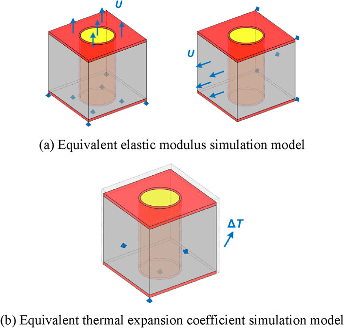
Figure 1. Equivalent simulation model. (A) Equivalent elastic modulus simulation model. (B) Equivalent thermal expansion coefficient simulation model.
Where Ez and Ex,y are the equivalent elastic moduli in the z and x-y directions respectively, νx-y is the equivalent Poisson’s ratio, σz and σx represents the stress in the z and x directions respectively, εz and εx,y are the tensile strains in the z and x directions (or y directions), and Fz and Fx are the support forces in the z and x directions respectively. Ax and Az are the cross-sectional areas of the unit model parallel to the x and z directions respectively.
The method for obtaining the equivalent coefficient of thermal expansion is as follows: set the normal degrees of freedom of the three adjacent surfaces of the model to 0, and set the temperature rise of ∆T, as shown in Figure 1B. The thermal expansion coefficient of the model is obtained from Equations 6, 7.
Where αx,y and αz are the thermal expansion coefficients in the x-y and z directions respectively, and
The calculation process for density and specific heat capacity is relatively simple. According to the definition of density shown in Equation 8.
Where ρeq is equivalent density, ρsi and ρcu are density of Si and Cu respectively. Introducing the volume ratio
Similarly, the formula for calculating the equivalent specific heat capacity can be obtained as Equation 10.
Where Ceq is equivalent specific heat capacity, CSi and Ccu are heat capacity of Si and Cu respectively.
2.2 Simplified model thermal simulation
In this paper, the Vega56 graphics card core, a representative 2.5D package manufactured by Advanced Micro Devices (AMD), has been meticulously chosen as the subject of study. Vega56 contains a graphics processing unit (GPU) die and two high bandwidth memory (HBM) dies. The three dies are interconnected with the Si interposer through CPBs. The Si interposer is interconnected with the substrate through C4 bumps, and the substrate is connected to the computer motherboard through BGA solder balls. Its appearance is shown in Figure 2A, and its cross-section is shown in Figure 2B.
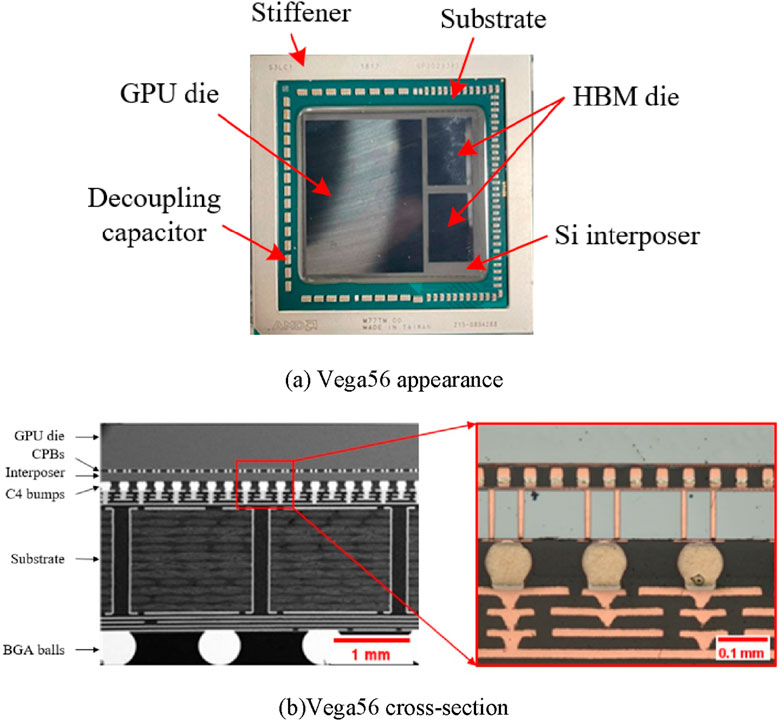
Figure 2. Vega56 appearance and cross-section. (A) Vega56 appearance. (B) Vega56 cross-section.
ABAQUS was used to conduct thermal simulation analysis of the model. The dimensions of each part of Vega56 are shown in Table 1. In light of the substantial quantity of CPBs, the construction of all individual CPBs would lead to exceedingly intricate models that demand considerable computational resources. In the thermal cycle, the dangerous solder joints of the chip are located at the center and corners, while the rest of the solder joints are relatively safe. Therefore, when constructing the model of CPBs in this paper, only the CPBs at the center of the chip and the four corners of the chip were constructed, and the rest was simplified using the equivalent model. In addition, the substrate, C4 bumps layer, and Si interposers were also simplified into rectangular shapes, resulting in the simulation model shown in Figure 3.
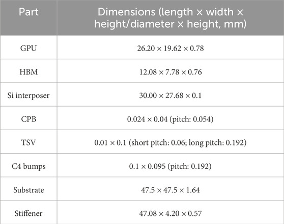
Table 1. Dimensions of Vega56.
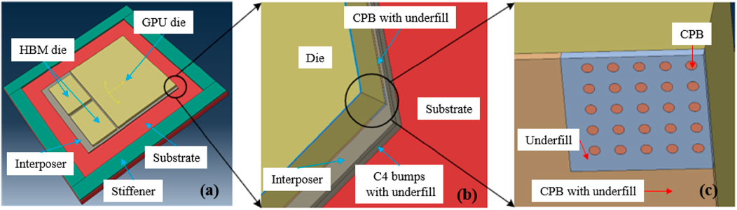
Figure 3. Simulation model of Vega56: (A) is overall view of the model; (B) shows the simplified model of interposer, C4 bumps with underfill and CPB with underfill; (C) shows the simplified model at corner of chip.
Based on the size and pitch of C4 bumps, CPBs, and TSVs, the volume ratio β could be calculated to be 20.532%, 15.514%, and 3.409%. Through (1)–(10), the material parameters of each structure in the model could be obtained, as shown in Table 2. The thermal conductivity of Cu, Si, and Interposers is temperature dependent, as shown in Table 3.
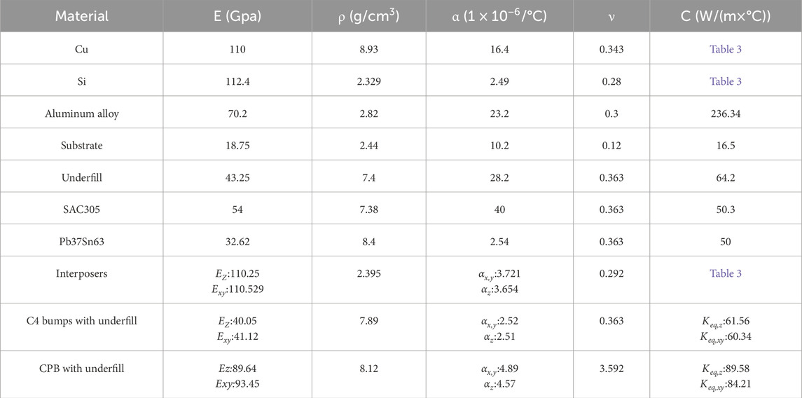
Table 2. Material parameters.
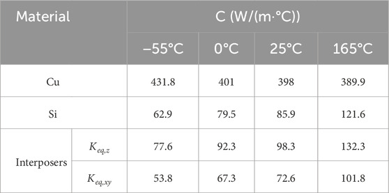
Table 3. Partial material thermal conductivity.
The simulation conditions for thermal cycling were −55°C∼165°C, with a temperature change rate of 10°C/min, a temperature retention time of 15 min, and a cycle period of 74 min. In the thermal cycling simulation, the initial temperature was set to 25°C, with a cycle time of 2 h per cycle, culminating in a total duration of 148 min for the thermal cycling regimen. The thermal cycle profile is illustrated in Figure 4. During the static analysis segment, the boundary conditions were meticulously defined to incorporate fixed restraints at the vertices of the substrate’s basal plane.
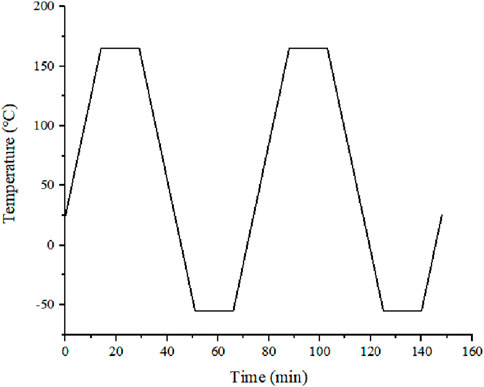
Figure 4. Thermal cycle curve.
Eight-node hexahedral solid elements were used for meshing. During the transient thermal analysis, the DC3D8 unit was used, and during the static analysis the C3D8R unit was used. For thin-layer structures, the number of meshes in the z direction was controlled to two layers of meshes at least. The meshing results are shown in Figure 5.
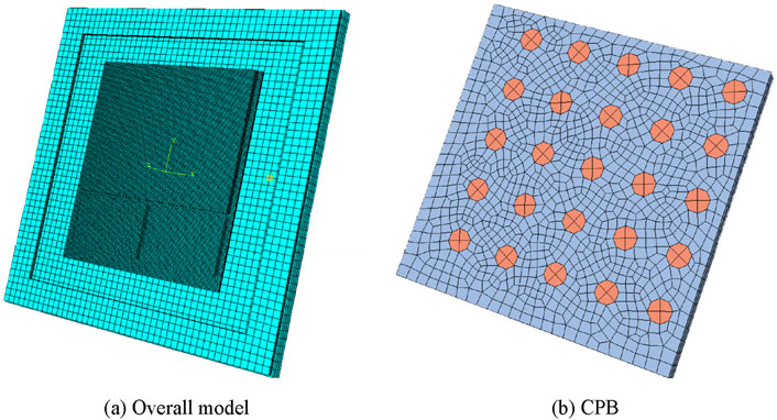
Figure 5. Meshing results of Vega56. (A) Overall model. (B) CPB.
The temperature field obtained from transient thermal simulation was put into static simulation as a predefined field to obtain the stress changes and warping deformation of the device under temperature cycling. The simulation results are shown in Figures 6A, B.
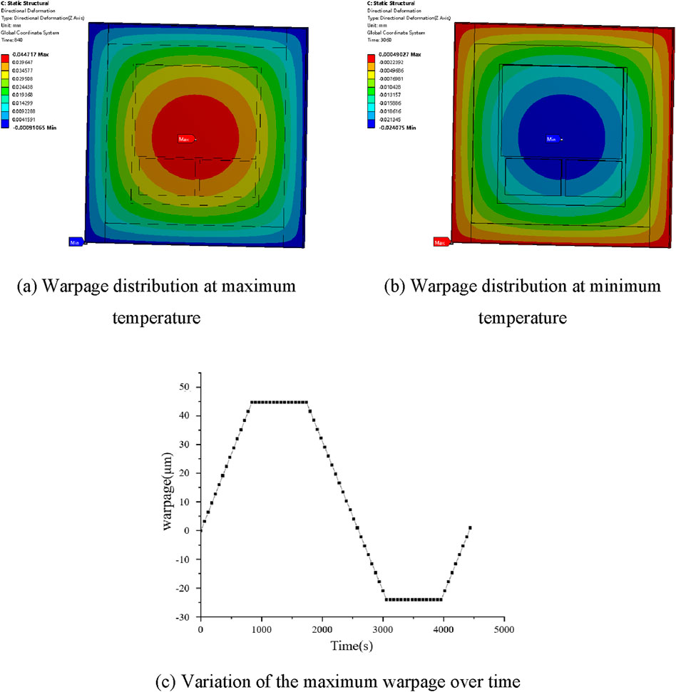
Figure 6. Warpage distribution and variation. (A) Warpage distribution at maximum temperature. (B) Warpage distribution at minimum temperature. (C) Variation of the maximum warpage over time.
It could be seen that during the heating stage, the chip mainly experienced arching warpage, while during the cooling stage, concave warpage occurred. At the maximum temperature, the warpage was the largest, reaching 44.717 μm. At the minimum temperature, the maximum concave warpage value was −24.075 μm. Figure 6C shows the variation of the maximum warpage over time within a cycle, which was similar to the temperature change. From the GPU stress distribution, it could be seen that the maximum stress point was located at the corners, mainly due to the smaller thermal expansion coefficient of the silicon chip and the larger thermal expansion coefficient of the substrate. Therefore, the warpage stress on the GPU was mainly caused by the warping of the substrate.
2.3 Verification of simulation
Shadow moire interferometry (Zhu et al., 2018; Du et al., 2019; Yeh et al., 2019) is a non-contact optical technology for warpage full-field measurement. It uses interference between a reference grating and its shadow on the sample to measure the relative vertical displacement of each pixel position. This technology was used for experimental verification of the overall model in this paper.
The equipment used in this article is TherMoire AXP produced by akrometrix, as shown in Figure 7A. The sample was heated using infrared heating, and was fixed on a standard glass block with an ultra-low coefficient of thermal expansion (CTE). The bending radius of the standard glass is known, which can be used to calibrate the influence of the external environment during the experiment. A thermocouple was installed next to the sample to detect temperature changes in the sample. The experimental setup is shown in Figure 7B.
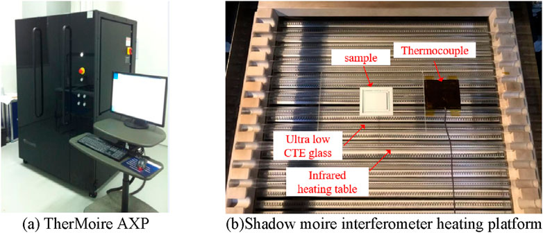
Figure 7. Equipment and experimental setup. (A) TherMoire AXP. (B) Shadow moire interferometer heating platform.
In order to maintain the device warpage in a steady state during experimentation, a heating rate of 10°C per minute was established, while the cooling rate was controlled to remain below −10°C per minute. The experimental setup included a maximum temperature of 165°C, with an ambient condition set at 25°C. Thermocouples were used to detect the surface temperature of the device in real time, and the temperature change curve was obtained as shown in Figure 8A.
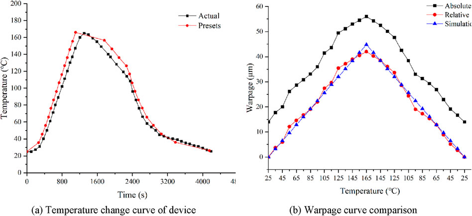
Figure 8. Temperature change curve and warpage curve comparison in the Verification experiment (A) Temperature change curve of device. (B) Warpage curve comparison.
During the experiment, the surface warpage of the sample was measured every 10 °C. Each measurement used the built-in three-step phase shift method of the equipment to obtain the surface warpage value. The experimental results are shown in Figure 8B.
The sample already had a warpage of 14 μm before heating, which perhaps caused by reflow soldering process. From Figure 8B, it could be seen that the initial warpage was arching warpage, that is, the center of the sample was higher than the four corners. As the temperature increases, the sample’s arching warpage further intensified, and when the maximum temperature was reached, the warpage value increased to a maximum of 56 μm. As the temperature decreases, the warpage value gradually decreased and eventually returned to the initial warpage value.
The temperature change curve obtained from the experiment was input to the previous simulation model as a boundary condition, and the warpage of the device surface was obtained, as shown in Figure 8B. The simulation results were in good agreement with the relative warpage measured in the experiment. The error at the maximum warpage was 6.47%, and the maximum error does not exceed 20%, with an average error of 8.93%. This indicates that the simplified modeling and simulation methods used in this paper have sufficient accuracy.
3 Simulation of fatigue crack propagation of CPB
3.1 Boundary load curve extraction
In the process of model refinement, the specific CPB located in close proximity to the apex of stress concentration within the overall model was precisely delineated. Subsequently, a detailed submodel encompassing this region of interest was extracted and delineated, as illustrated in Figure 9.
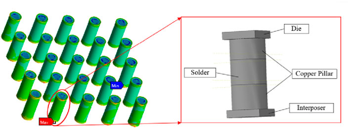
Figure 9. CPB submodel.
The solder layer material is SAC305, which is a viscoplastic material. Under thermal cycle conditions, plastic deformation and creep deformation mainly occur. The plastic constitutive model of SAC305 is shown in Equation 11.
where εp is equivalent plastic strain, Cp and np are both time-dependent material parameters (Cheng et al., 2008), as show in Table 4.
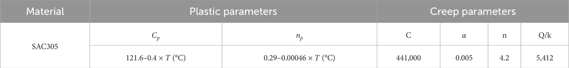
Table 4. Plastic and creep parameters of SAC305.
The steady-state creep constitutive model is a hyperbolic sine creep constitutive model (Glane et al., 2023) as Equation 12.
where Q is creep activation energy, T is temperature, n is stress exponent, k is Boltzmann constant, σ is applied stress, C and α are material constant, and
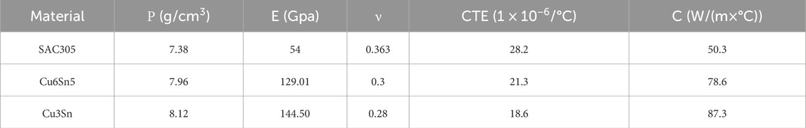
Table 5. Other material parameters.
Set the boundary conditions of the submodel as the displacement simulation results of the upper and lower surfaces. The boundary conditions for the submodel were established utilizing the displacement simulation outcomes obtained from the upper and lower surfaces. To achieve stable viscoplastic flow of the solder, the boundary conditions were cyclically loaded. The equivalent stress of the CPB was extracted for each cycle, with the stabilized equivalent stress serving as the boundary stress for subsequent analysis. Since the stress on the CPBs was mainly caused by the deformation of the dies, the external force was mainly on the upper and lower surfaces. The stress on the copper pillar was mainly in the z-axis direction, while the stress in the x and y directions was smaller. Consequently, in the simulation of fatigue crack propagation, the stress acting in the x and y directions was deemed negligible. The curve of the average principal stress on the outer surface of the copper pillar over time is shown in Figure 10.
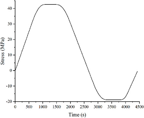
Figure 10. CPB boundary stress.
3.2 Thermal fatigue crack propagation simulation
Under the influence of temperature, due to the expansion movement of atoms, two intermetallic compounds, Cu6Sn5 and Cu3Sn, will gradually form between the solder and the copper pillar (Roy et al., 2022; Arafat et al., 2020). Generally speaking, the growth rate of Cu6Sn5 is greater than that of Cu3Sn, so Cu6Sn5 is prone to forming undulating wave shapes, while Cu3Sn generally forms relatively flat elongated shapes (An and Qin, 2016).
The IMC layer morphology characteristic parameters set in this paper are shown in Table 6. Rrms is the roughness of IMC layer, dave is the average thickness, λave is the average distance between wave paeks.

Table 6. Morphological characteristics of IMC layer.
Utilizing the MATLAB computational environment, a one-dimensional Gaussian random rough surface was meticulously modeled, with the explicit aim of synthesizing a stochastic rough surface profile that rigorously adhered to the specified parameters delineated within Table 6. Then, the rough surface data was imported into the CPB model, as shown in Figure 11A. During the crack propagation process, the CPE4R unit was used for simulation calculations. This unit can handle complex stress states and provide relatively high computational efficiency. The meshes are shown in Figure 11B.
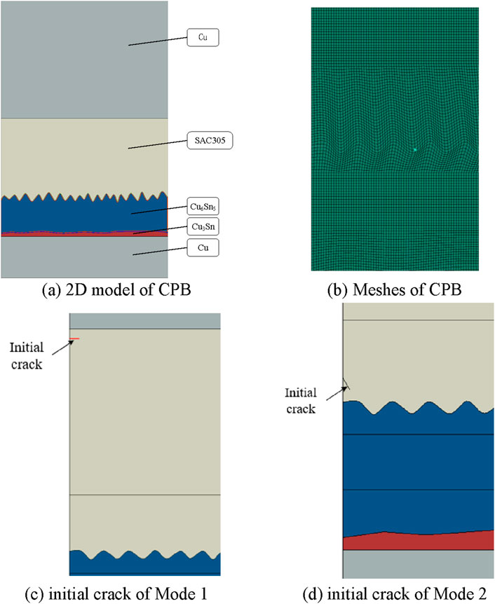
Figure 11. 2D model and Meshes of CPB and initial crack simulation model. (A) 2D model of CPB (B) Meshes of CPB (C) initial crack of Mode 1(D) initial crack of Mode 2.
According to the research in Li et al. (2020), there are two main ways of crack expansion in CPBs. Mode 1 is the crack propagation in SAC305, and Mode 2 is the crack propagation in Cu6Sn5, as shown in Figure 12.
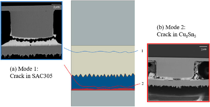
Figure 12. Schematic diagram of crack propagation: (A) Mode 1 crack is located in SAC305; (B) Mode 2 crack is located in Cu6Sn5 (Li et al., 2020).
Two initial cracks with length a0 = 0.5 μm were constructed respectively. The first initial crack was located in SAC305 and was a horizontal crack used to simulate Mode 1. The second initial crack was set at the interface between SAC305 and Cu6Sn5, with an inclination angle of 60°, to simulate Mode 2. The constructed simulation models are shown in Figures 11C, D.
Crack propagation can be roughly divided into three stages: crack initiation stage, stable propagation stage, and unstable propagation stage. The crack propagation rate during the stable propagation stage can be described using the Pairs formula (Rajaguru et al., 2019) as Equation 13.
where da/dN is the crack propagation rate; C and m are constants, which can be obtained by fitting experimental data; ΔK is the stress intensity factor amplitude.
The boundary load curve, as illustrated in Figure 10, was input into the model. The simulation of fatigue cracks was conducted through the direct cycle analysis step within the Abaqus software. Furthermore, the model parameters of the Paris formula was input, ensuring a comprehensive analysis of the fatigue crack propagation under the specified loading conditions. The parameters C and m in the Paris formula were obtained by fitting the experimental data in Tian et al. (2017), and the values of C and m are shown in Equation 14.
The fatigue crack propagation results of Mode 1 and Mode 2 are shown in Figure 13. And the relationship curve between the crack length a and the number of cycle N in Mode 1 and Mode 2 were established, as shown in Figure 14. In the crack propagation of Mode 1, as depicted in Figure 13A, the crack initiates from an initial flaw and propagates in a direction parallel to the upper surface of the CPB solder layer. This propagation continues until the crack traverses the entire solder layer, which is in close agreement with the Mode 1 crack propagation path for CPB as shown in Figure 12A. This behavior is likely attributed to creep damage in the solder layer proximate to the upper copper pillar. In contrast, for Mode 2 crack propagation, as illustrated in Figure 13B, the initial crack is situated near the IMC layer within the solder. The crack then crosses the interface between the SAC305 solder and the IMC layer, entering the Cu6Sn5 phase and propagating parallel to the lower surface of the copper pillar. This propagation continues until the crack laterally spans the entire IMC layer, closely aligning with the Mode 2 crack propagation path depicted in Figure 12B. Moreover, the crack propagation rate for Mode 2 was observed to be faster than that for Mode 1.
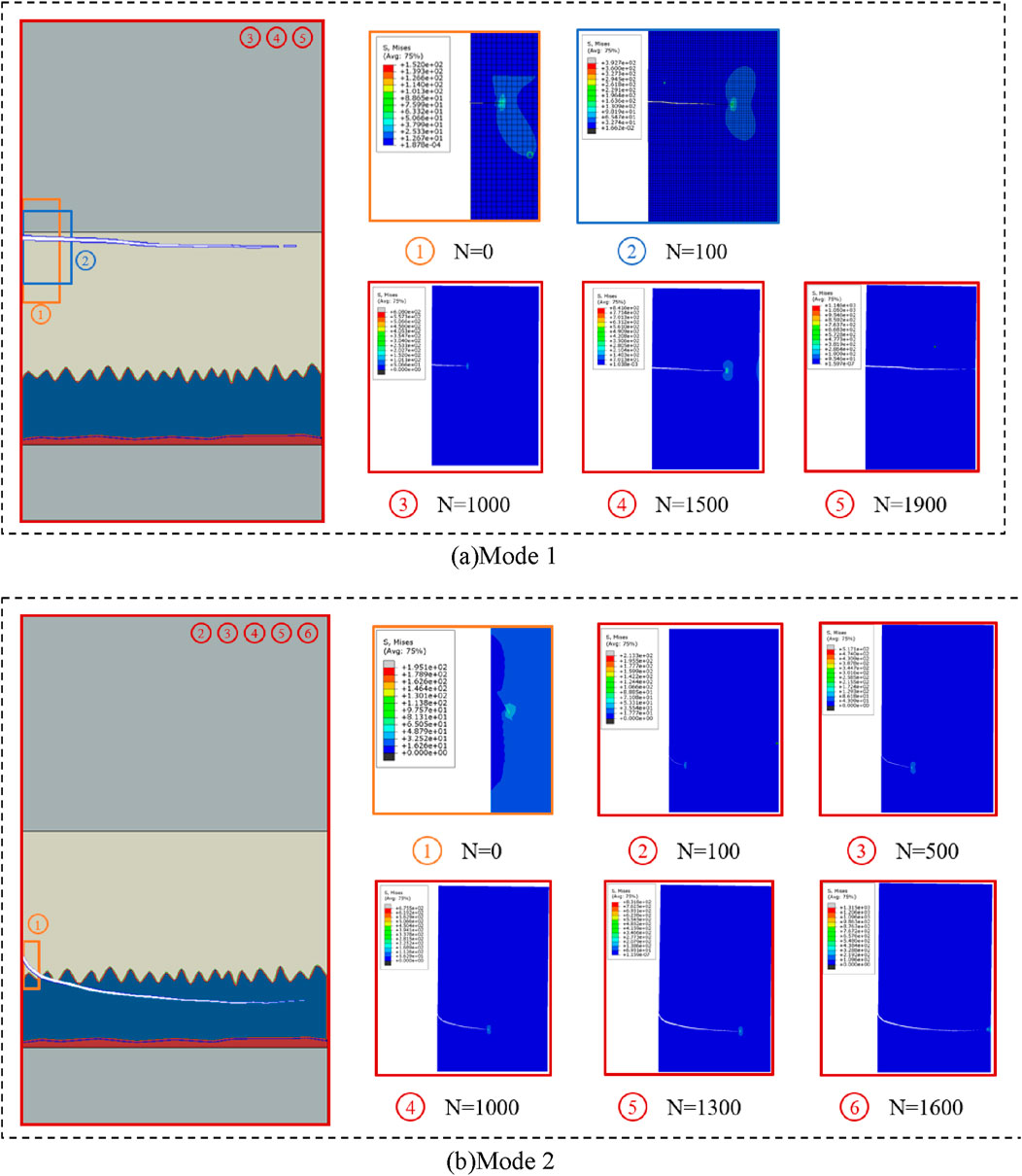
Figure 13. Fatigue crack propagation path of Mode 1 and Mode 2. (A) Mode 1. (B) Mode 2.
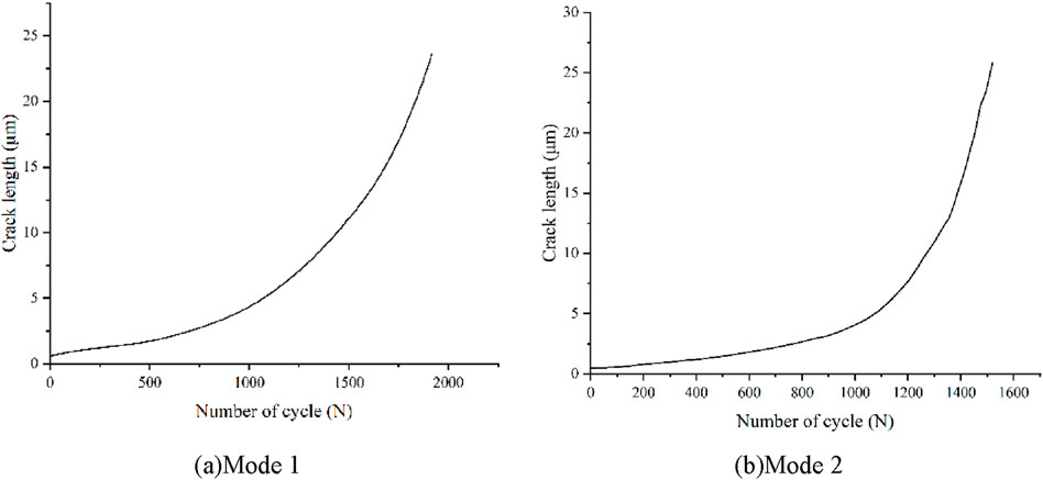
Figure 14. A–N curve of Mode 1 and Mode 2. (A) Mode 1. (B) Mode 2.
3.3 Fatigue lifetime prediction
The fatigue crack propagation life is the number of cycles that a crack undergoes from the initial length a0 to the critical length ac. The critical length ac is closely related to the stress intensity factor K at the crack tip and the fracture toughness KC of the material. When K ≥ KC, the crack will experience unstable propagation and quickly reach the life limit of the structure (Wang et al., 2023; Alter et al., 2020). The unstable propagation of cracks can be determined by Equation 15, 16.
where f is the geometric correction coefficient, and σmax is the maximum value of applied stress.
In this paper, f is 1.121, σmax is 43.13 MPa, and the fracture toughness of Cu6Sn5 is 0.481 MPa·m1/2 (Ghosh, 2004). The critical length of Mode 2 could be determined to be 21.78 μm. From the a-N curve in Figure 14, it could be concluded that the fatigue lifetime of Mode 2 is 1,470 cycles. When the number of cycles in Mode 1 reached 1900, the crack almost penetrated the entire CPB, indicating a fatigue lifetime of 1900 cycles.
4 Discussion
From the lifetime prediction results of Mode 1 and Mode 2, it could be seen that when the crack propagated in the IMC layer, the fatigue lifetime of CPB was shorter than that of the crack located in the solder, and the difference between the two was significant δ=(N1-N2)/N1 × 100% = 22.63%. This indicated that IMC had a significant influence on the fatigue lifetime of CPBs.
To investigate the effect of IMC layer thickness on the fatigue life of CPBs, this paper constructed simulation models with different IMC layer thicknesses. Due to the significant impact of the IMC layer, only the fatigue lifetime of Mode 2 was simulated. The a-N curves of CPBs with different IMC layer thicknesses are shown in Figure 15. And the fatigue lifetime prediction results of CPBs with different IMC layer thicknesses are shown in Table 7.
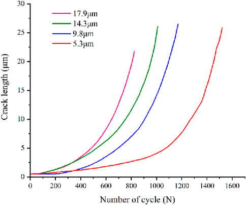
Figure 15. a-N curves of CPB with different IMC layer thicknesses.
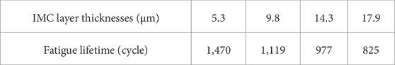
Table 7. Fatigue lifetime of CPBs with different IMC layer thicknesses.
From Figure 15, it can be seen that as the thickness of the IMC layer increased, the shape of the a-N curve remained basically unchanged, but the rate of crack propagation increased rapidly. It can also be seen from the lifetime prediction results that as the IMC increased, the fatigue lifetime of CPB will decrease significantly. When all the solder layers were converted to IMC, its fatigue lifetime decreased from 1,470 cycles to 825 cycles, a decrease of 43.88%.
These results indicate that the existence of the IMC layer accelerates the fatigue crack propagation of CPB, which will seriously reduce the fatigue lifetime of CPB, and the thickness of the IMC layer is one of the key influencing factors. Therefore, in the preparation process of CPB, it is necessary to choose appropriate process parameters to ensure that the IMC layer is thin, and attention should also be paid to the growth of the IMC during service.
5 Conclusion
This paper takes the CPBs in 2.5D package as the research object, and establishes a method for obtaining the lifetime of CPBs based on the basic theory of fatigue crack propagation. Using the extended finite element simulation method, the fatigue lifetime of CPBs with different IMC layer thicknesses under thermal cycling was simulated, and the influence of IMC layer thickness on the fatigue lifetime of CPBs was analyzed. Through the simulation results of fatigue crack propagation at CPBs, it was found that when the crack propagated in IMC, the fatigue lifetime of CPB was smaller than the lifetime when the crack propagated in the solder layer. This indicates that the influence of IMC layer on the fatigue lifetime of CPB is significant. And as the thickness of the IMC layer increases, the fatigue lifetime of the CPBs also significantly decreases. When the thickness of the IMC layer reaches 100% of the solder layer height, the fatigue lifetime of CPB will decrease by 43.88%. Therefore, when predicting the lifetime of the CPBs, it is necessary to consider the impact of the IMC layer. In addition, there may be defects such as voids in the IMC layer of CPBs, which have a certain impact on predicting crack propagation lifetime. In future research, initial defects can be incorporated into simulations to establish more accurate lifetime prediction methods.
Data availability statement
The raw data supporting the conclusions of this article will be made available by the authors, without undue reservation.
Author contributions
YZ: Conceptualization, Investigation, Methodology, Writing–review and editing. QL: Data curation, Software, Validation, Writing–original draft, Writing–review and editing. TM: Data curation, Formal Analysis, Validation, Writing–review and editing. SL: Data curation, Software, Writing–review and editing. XZ: Data curation, Software, Writing–review and editing.
Funding
The author(s) declare that no financial support was received for the research, authorship, and/or publication of this article.
Acknowledgments
We would like to thank the Reviewers for their suggestions which have resulted in substantial improvement to the quality of this manuscript.
Conflict of interest
The authors declare that the research was conducted in the absence of any commercial or financial relationships that could be construed as a potential conflict of interest.
Publisher’s note
All claims expressed in this article are solely those of the authors and do not necessarily represent those of their affiliated organizations, or those of the publisher, the editors and the reviewers. Any product that may be evaluated in this article, or claim that may be made by its manufacturer, is not guaranteed or endorsed by the publisher.
References
Ajay Kumar, P., and Dutta, I. (2018). Effect of intermetallic content on shear deformation of thin Sn-3.0Ag-0.5Cu solder micro-joints between copper substrates. J. Electron. Mater. 47 (9), 5488–5497. doi:10.1007/s11664-018-6434-z
Alter, A. L., Flader, I. B., Chen, Y., Ortiz, L. C., Shin, D. D., and Kenny, T. W. (2020). Characterization of accelerated fatigue in thick epi-polysilicon vacuum encapsulated MEMS resonators. J. Microelectromechanical Syst. 29 (6), 1483–1492. doi:10.1109/jmems.2020.3021947
An, T., and Qin, F. (2016). Relationship between the intermetallic compounds growth and the microcracking behavior of lead-free solder joints. J. Electron. Packag. 138 (1). doi:10.1115/1.4032349
Arafat, Y., Yang, H., Dutta, I., Kumar, P. A., and Datta, B. (2020). A model for intermetallic growth in thin Sn joints between Cu substrates: application to solder microjoints. J. Electron. Mater. 49 (5), 3367–3382. doi:10.1007/s11664-020-08019-8
Chen, C.-fu, and Wu, S.-T. (2015). Equivalent mechanical properties of through silicon via interposers – a unit model approach. Microelectron. Reliab. 55 (1), 221–230. doi:10.1016/j.microrel.2014.09.005
Chen, Y., Dai, W., Liu, Y., Chen, C., Tu, K., and Chen, G. (2022). Surface protrusion induced by inter-diffusion on Cu-Sn micro-pillars. Mater. and Des. 224, 111318. doi:10.1016/j.matdes.2022.111318
Cheng, F., Nishikawa, H., and Takemoto, T. (2008). Estimation of the thermal fatigue resistance and creep properties of the Co/Ni-bearing SAC305 lead-free solders by the strain rate change tensile test. Mater. Trans. 49 (7), 1503–1507. doi:10.2320/matertrans.mf200803
Chien, H.-C., Lau, J. H., Chao, Y.-L., Tain, R.-M., Dai, M.-J., Lo, W.-C., et al. (2011). “Estimation for equivalent thermal conductivity of silicon-through vias TSVs used for 3D IC integration,” in 2011 6th International Microsystems, Packaging, Assembly and Circuits Technology Conference (IMPACT), Taipei, Taiwan, October 19–21, 2011 (IEEE), 153–156. doi:10.1109/impact.2011.6117240
Dale, T., Singh, Y., Bernander, I., Subbarayan, G., Handwerker, C., Su, P., et al. (2020). Fatigue life of Sn3.0Ag0.5Cu solder alloy under combined cyclic shear and constant tensile/compressive loads. J. Electron. Packag. 142 (4). doi:10.1115/1.4048109
Du, H., Yu, J., and Zhang, S. (2019). “Self-calibrating phase shifting shadow moiré technique,” in 10th international symposium on precision engineering measurements and instrumentation, Kunming, China, August 08–10, 2018. Editors J. Tan, and J. Lin (Bellingham, WA: SPIE). doi:10.1117/12.2511924
Ghosh, G. (2004). Elastic properties, hardness, and indentation fracture toughness of intermetallics relevant to electronic packaging. J. Mater. Res. 19 (5), 1439–1454. doi:10.1557/jmr.2004.0193
Glane, S., Morozov, A., Müller, W. H., Hauck, T., Mazumder, G. R., Haq, M. A., et al. (2023). “Analytical and experimental studies on the damage evolution of SAC solder alloys,” in 2023 24th International Conference on Thermal, Mechanical and Multi-Physics Simulation and Experiments in Microelectronics and Microsystems (EuroSimE), Graz, Austria, April 16–19, 2023 (IEEE), 1–8. doi:10.1109/eurosime56861.2023.10100753
Gong, S., Chen, G., Qu, S., Duk, V., Xu, X., Shi, Q., et al. (2024). Effects of aging time and temperature on shear properties of Sn–Zn and Sn–Ag–Cu solder joints. J. Mater. Sci. Mater. Electron. 35 (11), 750. doi:10.1007/s10854-024-12440-8
Jing, X., Jiang, F., Xu, C., Xue, K., Dai, F., Li, Z., et al. (2014). “Investigation of temporary bonding and release processes for TSV with copper pillar bumps,” in 2014 15th International Conference on Electronic Packaging Technology, Chengdu, China, August 12–15, 2014 (IEEE), 86–89. doi:10.1109/icept.2014.6922602
Koo, J.-M., Kim, Y. N., Yoon, J. W., Ha, S. S., and Jung, S. B. (2007). Reliability of nickel flip chip bumps with a tin–silver encapsulation on a copper/tin–silver substrate during the bonding process. Microelectron. Eng. 84 (11), 2686–2690. doi:10.1016/j.mee.2007.05.026
Kwon, Y.-H., Bang, H. S., and Bang, H. S. (2016). Viscoplasticity behavior of a solder joint on a drilled Cu pillar bump under thermal cycling using FEA. J. Electron. Mater. 46 (2), 833–840. doi:10.1007/s11664-016-4970-y
Lancaster, A., and Keswani, M. (2018). Integrated circuit packaging review with an emphasis on 3D packaging. Integration 60, 204–212. doi:10.1016/j.vlsi.2017.09.008
Li, J., Zhang, Y., Zhang, H., Chen, Z., Zhou, C., Liu, X., et al. (2020). The thermal cycling reliability of copper pillar solder bump in flip chip via thermal compression bonding. Microelectron. Reliab. 104, 113543. doi:10.1016/j.microrel.2019.113543
Liu, E.-X., Wei, X.-C., and Li, E.-P. (2016). “2.5D methodologies for electronic package and PCB modeling: review and latest development,” in 2016 IEEE International Symposium on Electromagnetic Compatibility (EMC), Ottawa, ON, Canada, July 25–29, 2016 (IEEE), 801–805. doi:10.1109/isemc.2016.7571752
Long, Xu, Guo, Y., Su, Y., Siow, K. S., and Chen, C. (2023). Unveiling the damage evolution of SAC305 during fatigue by entropy generation. Int. J. Mech. Sci. 244, 108087. doi:10.1016/j.ijmecsci.2022.108087
Na, C.-Y., Jeon, B. M., Kim, J. W., Jung, W. S., Jeong, J. S., Cho, S. M., et al. (2022). Fabrication of 30 µm Sn microbumps by electroplating and investigation of IMC characteristics on shear strength. Electronics 12 (1), 144. doi:10.3390/electronics12010144
Rajaguru, P., Lu, H., and Bailey, C. (2019). Time integration damage model for Sn3.5Ag solder interconnect in power electronic module. IEEE Trans. Device Mater. Reliab. 19 (1), 140–148. doi:10.1109/tdmr.2019.2891949
Rao, L., Hu, F., Xu, P., Hu, A., Gao, L., Li, M., et al. (2016). “Research on the interfacial reaction and mechanism of Cu/Sn/Ni copper pillar bump,” in 2016 17th International Conference on Electronic Packaging Technology (ICEPT), Wuhan, China, August 16–19, 2016 (IEEE), 1045–1050. doi:10.1109/icept.2016.7583306
Roy, A., Luktuke, A., Chawla, N., and Ankit, K. (2022). Predicting the Cu6Sn5 growth kinetics during thermal aging of Cu-Sn solder joints using simplistic kinetic modeling. J. Electron. Mater. 51 (7), 4063–4072. doi:10.1007/s11664-022-09643-2
Su, S., Akkara, F. J., Thaper, R., Alkhazali, A., Hamasha, M., and Hamasha, S. (2019). A state-of-the-art review of fatigue life prediction models for solder joint. J. Electron. Packag. 141 (4). doi:10.1115/1.4043405
Tian, R., Tian, Y., Wang, C., and Zhao, L. (2017). Mechanical properties and fracture mechanisms of Sn-3.0Ag-0.5Cu solder alloys and joints at cryogenic temperatures. Mater. Sci. Eng. A 684, 697–705. doi:10.1016/j.msea.2016.12.058
Wang, L., Wu, L. C., and Wang, J. (2023). The characterization of low-k thin films and their fracture analysis in a WLCSP device. Microelectron. Reliab. 148, 115136. doi:10.1016/j.microrel.2023.115136
Watanabe, H. (2009). “Nanoelectronics devices: more CMOS, fusion CMOS and beyond CMOS,” in 2009 IEEE Asian Solid-State Circuits Conference, Taipei, Taiwan, November 16–18, 2009 (IEEE), 5–8. doi:10.1109/asscc.2009.5357243
Wong, H. (2021). “On the CMOS device downsizing, more moore, more than moore, and more-than-moore for more moore,” in 2021 IEEE 32nd International Conference on Microelectronics (MIEL), Nis, Serbia, September 12–14, 2021 (IEEE), 9–15. doi:10.1109/miel52794.2021.9569101
Yeh, H.-Y., Hsu, Y. K., Lee, J. Y., and Wei, A. C. (2019). Force-displacement measurement using simultaneous phase-shifting technique. Jpn. J. Appl. Phys. 58, SJJD02–SJ. doi:10.7567/1347-4065/ab24b9
Yu, S., Dai, J., and Li, J. (2024). Research on the reliability of interconnected solder joints of copper pillars under random vibration. J. Electron. Test. 40 (1), 107–116. doi:10.1007/s10836-024-06101-1
Zhang, P., Wang, D. W., Zhao, W. S., Su, J., You, B., and Liu, J. (2021). Multiphysics analysis and optimal design of compressible micro-interconnect for 2.5d/3D heterogeneous integration. Electronics 10 (18), 2240. doi:10.3390/electronics10182240
Zhang, X., Lin, J. K., Wickramanayaka, S., Zhang, S., Weerasekera, R., Dutta, R., et al. (2015). Heterogeneous 2.5D integration on through silicon interposer. Appl. Phys. Rev. 2 (2), 021308. doi:10.1063/1.4921463
Zhu, F., Lin, X., Zhang, W., Fan, J., and Liu, S. (2018). Morphology evaluation of microelectronic packaging substrates using shadow moiré technique. IEEE Access 6, 33099–33110. doi:10.1109/access.2018.2842199
Keywords: 2.5D package, copper pillar bump (CPB), IMC layer, extended finite element simulation, lifetime prediction
Citation: Zhou Y, Liu Q, Ma T, Li S and Zhang X (2024) Lifetime prediction of copper pillar bumps based on fatigue crack propagation. Front. Mater. 11:1470365. doi: 10.3389/fmats.2024.1470365
Received: 25 July 2024; Accepted: 21 August 2024;
Published: 02 September 2024.
Edited by:
Yutai Su, Northwestern Polytechnical University, ChinaReviewed by:
Canyu Liu, Huazhong University of Science and Technology, ChinaYanwei Dai, Beijing University of Technology, China
Copyright © 2024 Zhou, Liu, Ma, Li and Zhang. This is an open-access article distributed under the terms of the Creative Commons Attribution License (CC BY). The use, distribution or reproduction in other forums is permitted, provided the original author(s) and the copyright owner(s) are credited and that the original publication in this journal is cited, in accordance with accepted academic practice. No use, distribution or reproduction is permitted which does not comply with these terms.
*Correspondence: Qingsheng Liu, YnlsaXVxaW5nc2hlbmdAYnVhYS5lZHUuY24=