 Bo Wang
 Wangyun Li1,2*
- 1Guangxi Key Laboratory of Manufacturing System and Advanced Manufacturing Technology, School of Mechanical and Electrical Engineering, Guilin University of Electronic Technology, Guilin, China
- 2Flexible 3D System Integration Laboratory, Osaka University, Osaka, Ibaraki, Japan
The shear fatigue performance and fracture behavior of microscale ball grid array (BGA) structure Cu/Sn-3.0Ag-0.5Cu/Cu solder joints with different heights (500 μm, 300 μm, and 100 μm) with increasing current density (from 6.0 × 10³ to 1.1 × 10⁴ A/cm2) were investigated systematically. The results reveal that the fatigue life of solder joints decreases with increasing current density, while increasing with decreasing the height of solder joints. The location of fatigue fracture shifts from solder matrix to the interface between solder and intermetallic compound (IMC) layer for those with heights of 500 μm and 300 μm with increasing current density, in which the interfacial fracture is triggered by current crowding at the groove of the IMC layer and driven by mismatch strain at the solder/IMC layer interface; while, the fatigue fracture all occurs in the solder matrix for solder joints with a height of 100 μm. Moreover, the fracture in solder matrix of solder joints with heights of 500 μm and 300 μm exhibits an arc-shape fracture path, while a linear path for those with a height of 100 μm. These fracture paths are consistent with the concentration distribution region of plastic strain energy in solder joints.
1 Introduction
Solder joints provide mechanical support and electric interconnects between the chip and printed circuit board (PCB) in microelectronic devices, which has a critical impact on the functional performance and reliability of the entire device (Zhang et al., 2020; Bi et al., 2020; Wang et al., 2020). The reliability of solder joints largely depends on their service condition, and current stressing is one of the main service conditions of solder joints. Under current stressing, Joule heating will change the thermal condition, which causes the solder joints subjecting to shear strain due to differences in coefficient of thermal expansion (CTE) among each part in solder joint (Chen et al., 2022). With the fluctuation of power or temperature, the cyclic shear strain will be generated in solder joints, thus inducing shear fatigue, which is the main failure mode of the solder joints in service.
With the miniaturization of electronics, the size of solder joints decreases, resulting in an increase in the current density flowing in the solder joints. Previous studies have shown that current stressing has a significant impact on the fatigue life and fracture behavior of solder joints. In the fatigue and thermal cycling test of ball grid array (BGA) structure Cu/Sn-3.0Ag-0.5Cu/Cu solder joints, the lifetime of solder joints under current stressing with a current density of 1.154 × 10³ A/cm2 was 60% lower than those without current stressing (Zhang et al., 2021). Similar phenomenon also appear in millimeter-scaled lap-type Cu/Sn-3.5Ag-0.5Cu/Cu (Long et al., 2019), Cu/Sn-3.8Ag-0.5Cu/Cu solder joints (Jiao et al., 2019), microscale Cu/Sn-58Bi/Cu solder joints (Zuo et al., 2013), flip-chip Cu/Sn-3.8Ag-0.7Cu/Cu (Zhu et al., 2017; Gao et al., 2013) and Cu pillar Sn (Ma et al., 2016) solder joints, and their lifetime continuously decreased with increasing current density. In addition, the location and mode of fatigue fracture of solder joints under current stressing have also changed. For the flip-chip Cu/Sn-3.8Ag-0.7Cu/Cu solder joints, fracture tends to occur in the solder matrix near the solder/intermetallic compound (IMC) layer on the PCB side at a current density of 1.2 × 10⁴ A/cm2, while it tends to appear at solder/IMC layer interface at a current density of 1.5 × 10⁴ A/cm2 (Zhu et al., 2017). Moreover, the three distinct fracture modes can be observed in Cu/Sn-3.0Ag-0.5Cu/Cu solder joints, that is, fracture occurs in solder matrix without marked changes in solder microstructure (mode I); fracture occurs in solder matrix with obvious changes in solder microstructure (mode II); fracture occurs both in solder matrix and at solder/IMC layer interface (mode III) (Karppinen et al., 2013). While, in fatigue test of Cu/Sn-3.0Ag-0.5Cu/Cu solder joints under electro-thermal-vibration coupled loads, the fracture location changes gradually from solder/IMC layer interface to solder matrix with increasing temperature from 25°C to 100°C (Hu et al., 2005). In other words, there are three fracture modes, that is, fracture in solder matrix, mixed fracture in solder matrix and solder/IMC interface, and fracture in solder/IMC interface. In addition to current stressing, the solder joints with different sizes also exhibit different fatigue life and fracture behaviors. In the thermal cycle test of ceramic ball grid array (CBGA) components with different sizes (0.76 mm, 1.0 mm, and 1.3 mm), reducing the size of the solder joint is beneficial to reducing the stress and strain in the solder joint, and CBGA components with a size of 0.76 mm have the best thermal cycle reliability (Hu et al., 2005). Similar phenomena also occur in plastic ball grid array (PBGA) solder joints under board-level vibration conditions (Qi et al., 2011; She et al., 2019; Cui and Cheng, 2012) and BGA solder joints under board-level drop tests (Luan et al., 2005). However, in the random vibration fatigue tests of micro-scale chip scale package (CSP) solder joints and in the thermal cycling tests of quad flat package (QFP) solder joints, a contrary conclusion has been obtained, that is, the stress and strain in the solder joint increase with decreasing size of solder joints (Han et al., 2019; Fu and Wang, 2016). Moreover, the fatigue fracture of solder joints is also affected by joint size. In the shear fatigue test of BGA structure Cu/Sn-3.0Ag-0.5Cu/Cu solder joints, although both solder joints with a height of 300 μm and 500 μm fracture in the solder matrix, fracture location of smaller solder joints is closer to the solder/ICM layer interface (Qin et al., 2014b). However, the influence of size on the fatigue performance and fracture behavior of solder joints under current stressing is rarely investigated. The evolution mechanism of fatigue life and fracture behavior of solder joints with different sizes under current stressing needs further systematic and in-depth exploration.
In this study, the shear fatigue and fracture behavior of BGA structure Cu/Sn-3.0Ag-0.5Cu/Cu solder joints under current stressing were investigated. Considering that the height of solder joint, an important size parameter, has a significant impact on the mechanical properties and fracture behavior of solder joints (Wang et al., 2008), the study focuses on discussing the influence of change in height of solder joints on their fatigue performance to reveal the size effect of fatigue behavior. Moreover, the stress and strain state in solder joint was analyzed by the finite element (FE) method.
2 Experimental procedure and simulation method
2.1 Experimental procedure
In the study, the BGA structure Cu/Sn-3.0Ag-0.5Cu/Cu joints with different heights were fabricated and used. A bismaleimide triazine (BT) epoxy-based substrate with a surface finish of copper-organic solderability preservatives (Cu-OSP) was chosen for the fabrication. The opening diameter of the pad was 320 μm. During the fabrication, the height of solder joint (the distance between the upper and lower substrates) was controlled by using Cu wires with a diameter of 500 μm, 300 μm and 100 μm, respectively. The height of solder joint (h) corresponding to the diameter of solder ball (Dball) was: h = 500 μm, Dball = 650 μm; h = 300 μm, Dball = 500 μm; h = 100 μm, Dball = 300 μm. The fabrication procedure of the solder joint was the same with previous work (Wang et al., 2022c). The cross-sectional morphology and related dimensions of the prepared solder joints are shown in Figure 1; Table 1, respectively.
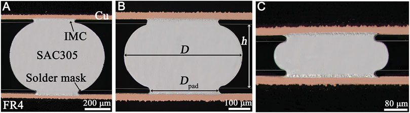
Figure 1. Cross-section morphology of solder joints with different heights: (A) h = 500 μm; (B) h = 300 μm; (C) h = 100 μm.
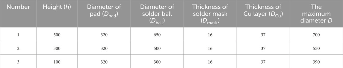
Table 1. Size parameters of solder joints with different heights (unit: μm).
The shear fatigue test was carried out using a dynamic mechanical analyzer (DMA Q800). A fixed gauge length of 18 mm was used when mounting the solder joints sample in the clamp of the DMA, to minimize the effect of substrate length on the shear fatigue behavior of solder joints. Before shear fatigue test, the direct current (DC) was applied to the solder joint for 3 min by a constant current power supply (ANS1560D) to achieve an equilibrium state in temperature.
The current density applied to the solder joint was 6.0 × 10³ A/cm2, 7.0 × 10³ A/cm2, 8.0 × 10³ A/cm2, 9.0 × 10³ A/cm2, 1.0 × 10⁴ A/cm2, 1.1 × 10⁴ A/cm2, respectively. After that, a cyclic shear load with displacement control mode was applied to the solder joint while keeping DC loading. The experimental schematic diagram is shown in Figure 2. The displacement amplitude of cyclic load applied to solder joints with a height of 500 μm, 300 μm, and 100 μm was ±25 μm, ±15 μm, and ±5 μm, respectively, which was equal to nominal shear strain amplitudes of 0.05 (γa = 0.05). The control waveform was a symmetrical trapezoidal wave with a dwell time of 3 s and a stress ratio of R = −1, as shown in Figure 3. The loading rate (or ramp rate in the symmetrical trapezoidal wave) was set as 3 μm/s. After test, the sample was characterized using a 3D measuring laser microscope (OLS4100) and a scanning electron microscope (SEM, Quanta 450, FEI) equipped with an energy-dispersive spectrometer (EDS).
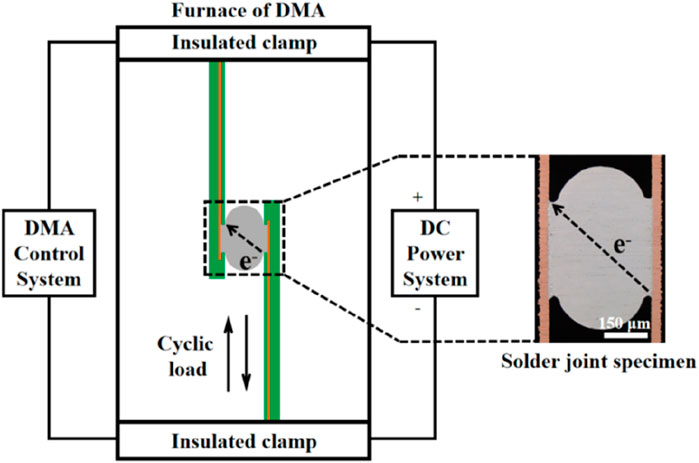
Figure 2. Schematic diagram of the experiment.
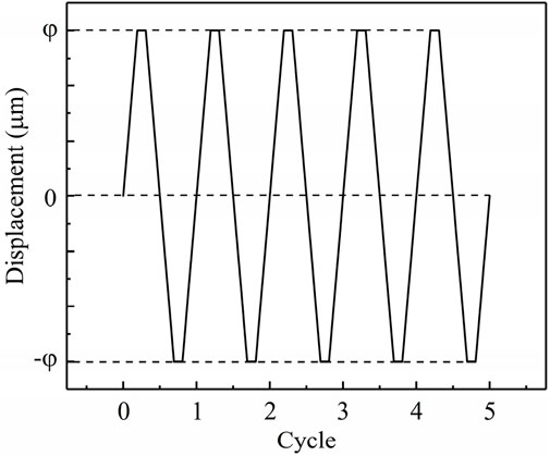
Figure 3. The loading waveform of cyclic shear load.
2.2 FE method
To characterize the magnitude and distribution of stress, strain and plastic strain energy in the solder joints, FE simulation using ANSYS multi-physics software platform was conducted. The dimensions of the FE model of solder joints are determined according to the actual size of solder joint, which can be referred to Figure 1; Table 1. According to the EDS results shown in Section 3.2 of the results section, the interfacial IMC between Sn-3.0Ag-0.5Cu solder and Cu pad is Cu6Sn5. The physical parameters of Cu, Sn-3.0Ag-0.5Cu solder, Cu6Sn5, and substrate material (FR4) are given in Table 2. Moreover, Anand model is used as the material constitutive model to simulate the nonlinear material behavior of the viscoplastic Sn-3.0Ag-0.5Cu solder in FE simulation, and the parameters of the model are given in Table 3. The computational mesh model of solder joints with different heights is shown in Figure 4.
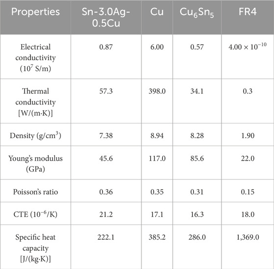
Table 2. Materials properties for FE simulation (Wang et al., 2022b).
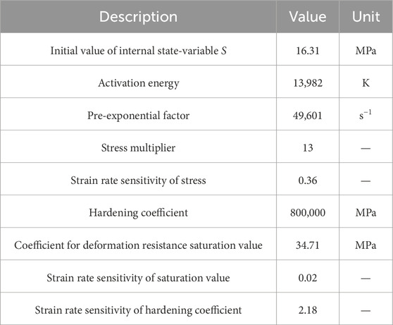
Table 3. Parameters of Anand model of Sn-3.0Ag-0.5Cu (Wang et al., 2022a).
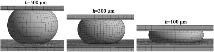
Figure 4. Computational mesh model of solder joints with different heights.
3 Results
3.1 Fatigue life of solder joints
The fatigue life of solder joints with different heights under current stressing is shown in Figure 5. Obviously, the fatigue life of solder joints increases monotonically with decreasing height of solder joint. Moreover, solder joints at all heights show a lower fatigue life under current stressing with a larger current density.
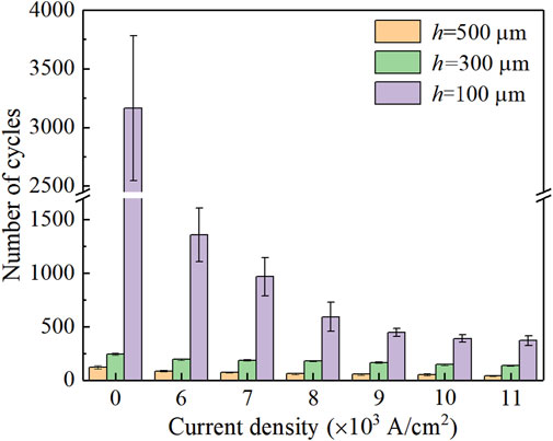
Figure 5. The fatigue life of solder joints with different heights under current stressing.
3.2 Fatigue fracture behavior of solder joints
The fracture surface morphologies of solder joints with a height of 500 μm under different current densities are shown in Figure 6. Without current stressing, the fatigue fracture occurs in the solder matrix, and the solder at the center of the fracture exhibits a prominent protrusion morphology, as shown in Figure 6A. This fracture morphology is similar to that of BGA structure solder joints reported in literature (Qin et al., 2014b). When solder joints under current stressing with a current density of 6.0 × 10³ A/cm2, the fracture surface morphology is similar to that without current stressing. While, a local melting can be observed on fracture surface, as shown in Figure 6B. As the current density further increases to 1.0 × 10⁴ A/cm2, besides local solder melting, some particles can be observed on the fracture surface, as shown in Figures 6C–J. When the current density reaches 1.1 × 10⁴ A/cm2, the whole fracture surface of solder joints is covered with particles, as shown in Figures 6K, L. The EDS analysis results in Figures 6M, N indicate that these particles are Cu6Sn5. Accordingly, the fatigue fracture of solder joints began to occur at solder/IMC layer interface under current stressing with a current density of 7.0 × 10³ A/cm2, while a whole interfacial fracture occurred under current stressing with a current density of 1.1 × 10⁴ A/cm2. In other words, the fatigue fracture location of solder joints transfers gradually from the solder matrix to the solder/IMC layer interface with increasing current density.
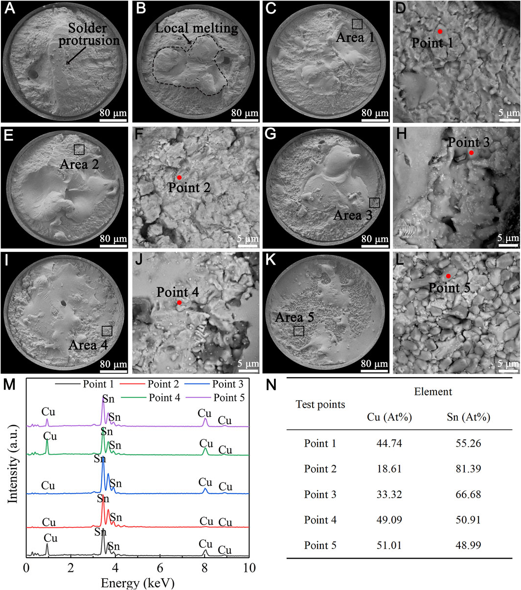
Figure 6. Fracture surface morphologies of solder joints (h = 500 μm) under different current densities: (A) 0 A/cm2; (B) 6.0 × 10³ A/cm2; (C) 7.0 × 10³ A/cm2; (D) enlarged view of area 1; (E) 8.0 × 10³ A/cm2; (F) enlarged view of area 2; (G) 9.0 × 10³ A/cm2; (H) enlarged view of area 3; (I) 1.0 × 10⁴ A/cm2; (J) enlarged view of area 4; (K) 1.1 × 10⁴ A/cm2; (L) enlarged view of area 5; (M) EDS results of point 1 to point 5; (N) atomic ratio of elements in point 1 to point 5.
The fracture surface morphologies of solder joints with a height of 300 μm under different current densities are shown in Figure 7. Without current stressing, the morphological characteristics of fracture surface of solder joints are similar to those of solder joints with a height of 500 μm, as shown in Figure 7A. When solder joints under current stressing with the current density increases from 6.0 × 10³ to 8.0 × 10³ A/cm2, local melting of solder occurs on the fracture surface while the morphological characteristics are similar to those without current stressing, as shown in Figures 7B–D. As the current density further increases to 9.0 × 10³, 1.0 × 10⁴ and 1.1 × 10⁴ A/cm2, the exposed particles were observed on the fracture surface, as shown in Figures 7E–J. According to the EDS analysis results in Figures 7K, L, these particles are consistent with those observed in fracture surface of solder joints with a height of 500 μm, that is Cu6Sn5, which indicates that the fatigue fracture location of solder joints with a height of 300 μm also undergoes a transition from solder matrix to solder/IMC layer interface with increasing current density. However, it is worth noting that interfacial fracture occurs at a current density of 9.0 × 10³ A/cm2 for solder joints with a height of 300 μm, which is higher than that (7.0 × 10³ A/cm2) in solder joints with a height of 500 μm. Moreover, fracture surface of solder joints with a height of 300 μm does not exhibit a complete interfacial fracture at a current density of 1.1 × 10⁴ A/cm2, which is different from that in solder joints with a height of 500 μm.
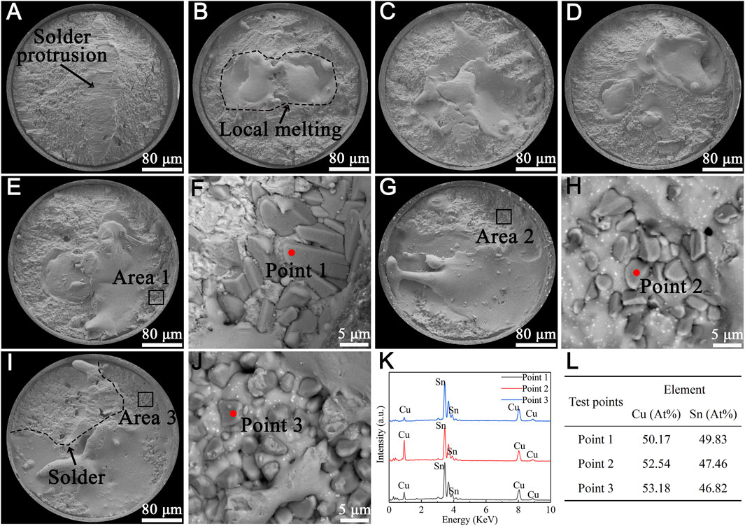
Figure 7. Fracture surface morphologies of solder joints (h = 300 μm) under different current densities: (A) 0 A/cm2; (B) 6.0 × 10³ A/cm2; (C) 7.0 × 10³ A/cm2; (D) 8.0 × 10³ A/cm2; (E) 9.0 × 10³ A/cm2; (F) enlarged view of area 1; (G) 1.0 × 10⁴ A/cm2; (H) enlarged view of area 2; (I) 1.1 × 10⁴ A/cm2; (J) enlarged view of area 3; (K) EDS results of point 1 to point 3; (L) atomic ratio of elements in point 1 to point 3.
The fracture surface morphologies of solder joints with a height of 100 μm under different current densities are shown in Figure 8. Without current stressing, the fatigue fracture occurs in the solder matrix, and exhibits a relatively flat morphology, as shown in Figure 8A, which is significantly different from the solder protrusion morphology observed in solder joints with a height of 500 μm or 300 μm. When solder joints under current stressing with a current density of 6.0 × 10³ A/cm2, the morphological characteristics of fracture surface of solder joints are similar to those without current stressing, while the local melting of solder can be observed on fracture surface, as shown in Figure 8B. With the current density further increasing from 7.0×10³ to 1.1 × 10⁴ A/cm2, the fracture location of solder joints remains in solder matrix, as shown in Figures 8C–G.
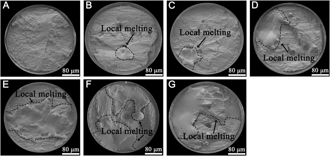
Figure 8. Fracture surface morphologies of solder joints (h = 100 μm) under different current densities: (A) 0 A/cm2; (B) 6.0 × 10³ A/cm2; (C) 7.0 × 10³ A/cm2; (D) 8.0 × 10³ A/cm2; (E) 9.0 × 10³ A/cm2; (F) 1.0 × 10⁴ A/cm2; (G) 1.1 × 10⁴ A/cm2.
According to the observation results of fracture surface of solder joints, the fatigue fracture behavior of solder joints with a height of 500 μm or 300 μm under current stressing is essentially different from that of solder joints with a height of 100 μm. In order to further figure out the difference, the fracture cross-section morphology of solder joints was analyzed, as shown in Figure 9. For the solder joints with a height of 500 μm without current stressing, the distance between the fracture location and the Cu pad is larger than thickness of solder mask, and the fracture path shows an arc-shape, as shown in Figure 9A, which is consistent with the solder protrusion morphology observed in Figure 6A. When the solder joints under current stressing with a current density of 6.0 × 10³ A/cm2, the distance from the fracture location to the Cu pad decreases compared to those without current stressing, while fracture path still presents an arc-shape, as shown in Figure 9B. As current density further increases to 1.1 × 10⁴ A/cm2, the fracture occurs in solder/IMC interface, indicating that the crack growth path is parallel to the substrate plane, as shown in Figure 9C. Moreover, it was observed that the fracture surface of solder joints was mainly composed of IMC grains and a small amount of solder at a current density of 1.1 × 10⁴ A/cm2, which was due to the complete interfacial fracture occurred at this current density. The small amount of solder observed is caused by the molten solder covering the surface of IMC layer. When the height of solder joints decreases to 300 μm, the fracture path presents an arc-shape consistent with that of solder joints with a height of 500 μm without or under current stressing with a current density of 6.0 × 10³ A/cm2, while the distance between the fracture location and the Cu pad decreases, as shown in Figures 9D, E. When solder joints under current stressing with a current density of 1.1 × 10⁴ A/cm2, the exposed IMC grains can be observed near the solder mask, and fracture mainly occurs in the solder matrix, as shown in Figure 9F. Moreover, the distance between the fracture location and the Cu pad further decreases. As the height of solder joints further decreases to 100 μm, the distance from the fracture location to the Cu pad is almost equal to the thickness of the solder mask without current stressing, and the fracture surface exhibits a relatively flat fracture morphology, which indicates that the crack growth path is parallel to the substrate plane, as shown in Figure 9G. When solder joints under current stressing with a current density of 6.0 × 10³ A/cm2, the fracture characteristics are similar to those without current stressing, while the distance from the fracture location to the Cu pad decreases, as shown in Figure 9H. As the current density increases to 1.1 × 10⁴ A/cm2, the distance from the fracture location to the Cu pad is further reduced, while fracture still occurs in solder matrix, as shown in Figure 9I, which indicates that the increase of current density leads to the fracture location of solder joints transferring gradually to the near substrate interface.
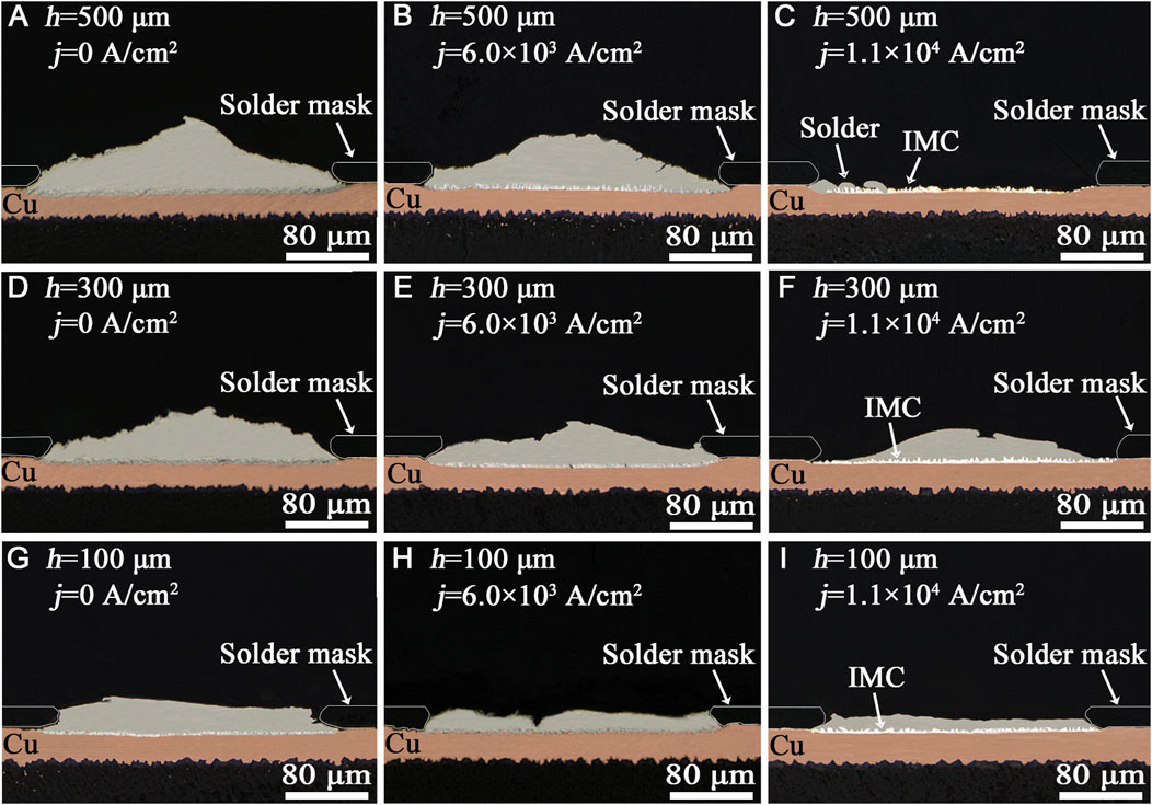
Figure 9. Cross-section morphologies (near substrate side) of solder joints under current stressing: (A) h = 500 μm, j = 0 A/cm2; (B) h = 500 μm, j = 6.0 × 10³ A/cm2; (C) h = 500 μm, j = 1.1 × 10⁴ A/cm2; (D) h = 300 μm, j = 0 A/cm2; (E) h = 300 μm, j = 6.0 × 10³ A/cm2; (F) h = 300 μm, j = 1.1 × 10⁴ A/cm2; (G) h = 100 μm, j = 0 A/cm2; (H) h = 100 μm, j = 6.0 × 10³ A/cm2; (I) h = 100 μm, j = 1.1 × 10⁴ A/cm2.
Accordingly, there is a similar fracture behavior for the solder joints with a height of 500 μm and 300 μm, that is, the fracture location transitions gradually from the solder matrix to the solder/IMC interface with increasing current density, and the fracture path shows an arc-shape. For the solder joints with a height of 100 μm, the fracture occurs in the solder matrix and transitions gradually to the near substrate interface with increasing current density, and the fracture path is parallel to the substrate plane.
4 Discussion
4.1 The influence mechanism of current stressing and height on fatigue life of solder joints
4.1.1 Influence mechanism of current stressing
The fatigue failure process of solder joints can be divided into two stages: fatigue crack initiation and fatigue crack propagation. Therefore, the ultimate fatigue life (N) of solder joints is the sum of the life before crack initiation (Ni) and life for crack propagation (Np), which can be expressed as:
in Equation 1, the life before crack initiation (Ni) is the number of cycles corresponding to accumulated plastic strain in solder joint reaching the critical value (pD). Based on continuum damage mechanics theory, Ni can be expressed as (Lemaitre and Desmorat, 2005):
where εpa is the plastic strain amplitude. During the fatigue crack propagation process, the crack propagation rate of BGA structure Cu/Sn-3.0Ag-0.5Cu/Cu solder joints can be expressed as (Qin et al., 2014a):
where vp is the crack propagation rate, AD is the area of fatigue crack propagation, ρ is the linear correlation coefficient, K is the material cyclic strength coefficient, Rv is the stress triaxiality function, E is the elastic modulus, S is the internal state-variable, s0 is the initial value of S, n is the strain rate sensitivity of saturation value. According to Equation 3, the life for crack propagation (Np) can be expressed as:
where A0 is the characteristic area, which refers to the area of fatigue crack propagation when failure or complete fracture. Considering that the parameters such as the K, Rv, E, S, and ρ are related to the material and structure of solder joint, therefore, the fatigue life of the solder joint mainly depends on the plastic deformation during the fatigue process and the characteristic area at complete fracture according to Equations 2, 4. Based on the unified constitutive model, the plastic strain rate (
where A is the pre-exponential factor, m is the strain rate sensitivity, Q is the activation energy, R is the universal gas constant, T is the working absolute temperature, and ξ is the material constant. When solder joint is subjected to current stressing, Equation 5 can be rewritten as:
where β is a constant, and j is the current density. For the BGA structure Cu/Sn-3.0Ag-0.5Cu/Cu solder joints, the temperature (T) in solder joint is related to the current density as follows (Wang et al., 2022c):
where ρR is the resistivity of the Sn-3.0Ag-0.5Cu solder, As is the cross-sectional area of the solder joint, H is the height of the solder joint, t is the current stressing time, h is the heat transfer coefficient, Sq is the surface of heating transfer, C is the specific heat, M is the mass of solder matrix and Ta is the ambient temperature. According to Equations 5, 6, when solder joints under current stressing, the activation energy Q decreases to (Q-βj2). At the same time, the temperature T in solder joint increases according to Equation 7, which induces a larger plastic deformation rate in the solder joint, thus resulting in a larger plastic deformation (Fu et al., 2016). According to Equations 2, 4, larger plastic deformation will lead to a lower Ni and Np, that is a lower fatigue life N. Therefore, the fatigue life of solder joints under current stressing is lower than that without current stressing, and further decreases with increasing current density.
4.1.2 Influence mechanism of height of solder joints
Based on the current experimental conditions, changes in solder joint height will cause a change in volume and shape of solder joint, resulting in different stress triaxiality (Jayabalan et al., 2019). The stress triaxiality function (Rv) can be expressed as (Qin et al., 2014a):
where v is the Poisson’s ratio, and Rσ is the stress triaxiality. For the BGA structure Cu/Sn-3.0Ag- 0.5Cu/Cu solder joints under shear load, the Rσ increases with increasing height (Qin et al., 2014b). Combining Equations 4, 8, an increase in Rσ leads to an increase in Rv, resulting in a decrease in fatigue propagation life Np. Moreover, the stress and strain of solder joints with different heights with/without current stressing were obtained through experimental measurements, and saturation hysteresis loops were plotted as shown in Figure 10. Obviously, the area of saturation hysteresis loops of solder joints with 500 µm height is the largest with/without current stressing, and decreases with decreasing height of the solder joint. It means that the solder joints with a larger height suffer greater damage, and thus have a lower fatigue life.
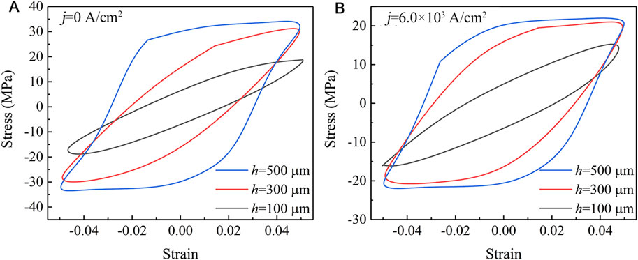
Figure 10. The stress-strain curves (third cycle loading) of solder joints with different heights under current stressing: (A) j = 0 A/cm2; (B) j = 6.0 × 10³ A/cm2.
4.2 Fatigue fracture mechanism of solder joints
Previous studies have shown that the fracture behavior of BGA structure solder joints under current stressing is related to the current density distribution, stress and strain state in the solder joints (Wang et al., 2022b; Wang et al., 2022c). The change in solder joint height will cause changes in current density, stress and strain distribution in solder joint, leading to changes in path and mode of fracture of solder joint. Firstly, the current density distribution in solder joints with different heights was calculated through finite element simulation. It was found that the severe current crowding occurs at the electron flow entrance and exit corners of solder joints, and the current density at the crowding area increases with increasing height of solder joints, as shown in Figure 11. Due to current crowding effect, a significant strain mismatch occurs at the solder/IMC layer interface, and increases with increasing height of solder joint, as shown in Figure 12. The strain mismatch at solder/IMC layer provides a driving force for the occurrence of interfacial fracture of solder joints. Therefore, interfacial fracture is prone to occur in solder joints with larger heights under current stressing. Secondly, through simulation of the stress distribution in solder joints, it was found that the stress concentration region gradually transfers from solder matrix to the substrate with increasing height of solder joints, and occurs at the solder/IMC layer interface when height reaches 500 μm, as shown in Figure 13. It indicates that the fracture location of solder joints with larger heights is more likely to occur at the solder/IMC interface layer.
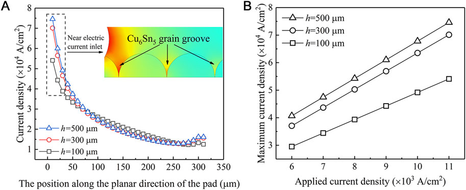
Figure 11. (A) Current density at IMC groove under a current density of 1.1 × 10⁴ A/cm2; (B) statistics of the maximum current density at IMC grooves with different applied current densities.
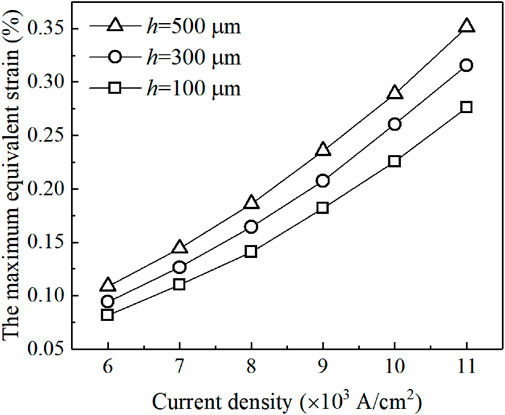
Figure 12. The maximum equivalent strain at solder/IMC layer interface of solder joints with different heights.
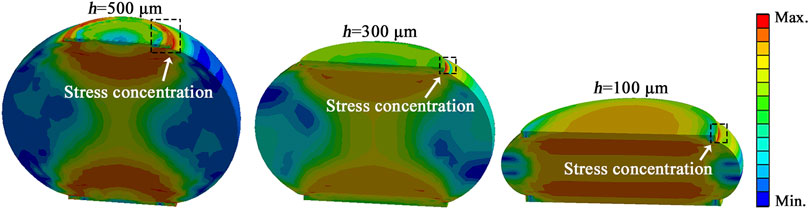
Figure 13. Von Mises stress distribution of solder joints with different heights under a current density of 6.0 × 10³ A/cm2.
In addition to interfacial fracture, the change in height of solder joints also affects the fracture behavior that occurs in the solder matrix. According to the observation of the fracture path (see Figure 9), the fracture of solder joints with different heights in the solder matrix presents two types, as shown in Figure 14. Type I, the crack propagates along the path parallel to the cyclic shear loading direction until fractured completely, as shown in Figure 14A. Type II, the crack propagates into the solder matrix and presents an arc-shape path, as shown in Figure 14B. Due to the viscoplastic characteristics of Sn-3.0Ag-0.5Cu solder, the plastic strain energy can be considered as the energy stored in the solder, which can provide a driving force for the generation and accumulation of damage, crack initiation and propagation (Zappalorto and Lazzarin, 2011). Therefore, the cracks in the solder matrix usually propagate along the region where the plastic strain energy distribution is concentrated. The distribution of plastic strain energy in solder joints with different heights is shown in Figure 15. For the solder joints with a height of 100 μm, the plastic strain energy is concentrated at the edge of solder, where is in contact with the solder mask. While, for the solder joint with a height of 300 μm and 500 μm, the plastic strain energy is concentrated in the solder matrix, and the concentration region presents an arc-shape. Accordingly, the former mainly exhibits type I fracture, while the latter mainly exhibits type II fracture.
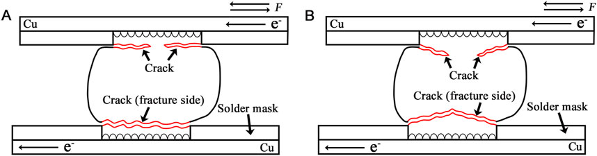
Figure 14. Two types of fatigue fracture occurring in solder matrix: (A) fracture along the loading direction (substrate); (B) arc-shape fracture.
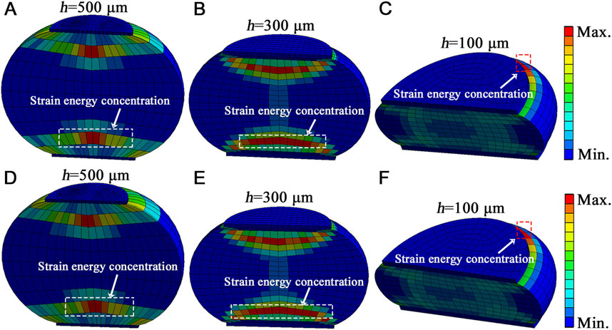
Figure 15. The plastic strain energy density distribution of solder joints with different heights under current stressing: (A) h = 500 μm, j = 0 A/cm2; (B) h = 300 μm, j = 0 A/cm2; (C) h = 100 μm, j = 0 A/cm2; (D) h = 500 μm, j = 6.0 × 10³ A/cm2; (E) h = 300 μm, j = 6.0 × 10³ A/cm2; (F) h = 100 μm, j = 6.0 × 10³ A/cm2.
5 Conclusion
The shear fatigue and fracture behavior of microscale BGA structure Cu/Sn-3.0Ag-0.5Cu/Cu solder joints with different heights under current stressing were investigated. The conclusions can be summarized as follows:
(1) The shear fatigue life of solder joints decreases with increasing current density, while increases with decreasing height of solder joints.
(2) The fatigue fracture location of solder joints gradually transfers from solder matrix to solder/IMC layer interface with increasing current density and height of solder joints.
(3) The current crowding and strain mismatch at solder/IMC layer interface increases with increasing current density and height of solder joints, which are the driving forces for the initiation and propagation of interfacial cracks, respectively.
(4) The propagation path of fatigue cracks in the solder matrix was along the plastic strain energy concentration area, which gradually changed from an arc-shape to a line shape parallel to the loading direction with decreasing height of solder joints.
Data availability statement
The original contributions presented in the study are included in the article/supplementary material, further inquiries can be directed to the corresponding authors.
Author contributions
BW: Conceptualization, Data curation, Writing–original draft. WL: Conceptualization, Funding acquisition, Writing–review and editing. KP: Conceptualization, Funding acquisition, Writing–review and editing. WH: Data curation, Writing–review and editing. YG: Data curation, Writing–review and editing.
Funding
The author(s) declare that financial support was received for the research, authorship, and/or publication of this article. This work was supported by the National Natural Science Foundation of China under Grant No. 52365042; Guangxi Key Laboratory of Manufacturing System and Advanced Manufacturing Technology under Grant No. 23354S009; Project for Enhancing Young and Middle-aged Teacher’s Research Basis Ability in Colleges of Guangxi under Grant No. 2024KY0220.
Conflict of interest
The authors declare that the research was conducted in the absence of any commercial or financial relationships that could be construed as a potential conflict of interest.
Publisher’s note
All claims expressed in this article are solely those of the authors and do not necessarily represent those of their affiliated organizations, or those of the publisher, the editors and the reviewers. Any product that may be evaluated in this article, or claim that may be made by its manufacturer, is not guaranteed or endorsed by the publisher.
References
Bi, X. Y., Hu, X. W., and Li, Q. L. (2020). Effect of Co addition into Ni film on shear strength of solder/Ni/Cu system: experimental and theoretical investigations. Mater. Sci. Eng. A 788, 139589. doi:10.1016/j.msea.2020.139589
Chen, G., Zhao, X. C., and Wu, H. (2017). A critical review of constitutive models for solders in electronic packaging. Adv. Mech. Eng. 9 (8), 168781401771497–21. doi:10.1177/1687814017714976
Chen, Y. L., Li, F., Li, K., Li, X., Liu, M., and Liu, G. (2022). Thermal fatigue reliability improvement of leadless ceramic chip carrier solder joints. Microelectron. Reliab. 132, 114532. doi:10.1016/j.microrel.2022.114532
Cui, H. P., and Cheng, E. Q. (2012). Random vibration analysis of PBGA solder joints with different structure parameters. Electron. Compon. Mater. 31, 44–46. doi:10.14106/j.cnki.1001-2028.2012.02.017
Fu, H. P., and Wang, K. (2016). Simulation of size effect on solder joint thermal cycle reliability. Electron. Process Technol. 37, 149–152. doi:10.14176/j.issn.1001-3474.2016.03.007
Fu, N. J., Suhling, J. C., and Lall, P. (2016). Cyclic stress-strain behavior of SAC305 lead free solder: effects of aging, temperature, strain rate, and plastic strain range. IEEE Electron. Compon. Technol. Conf., 1119–1127. doi:10.1109/ECTC.2016.345
Gao, F., Zhu, Q. S., Zheng, K., Liu, Z. Q., Guo, J. D., Zhang, L., et al. (2013). Failure of chip sized packaging (CSP) under coupling fields of electrical current and thermal cycle. Int. Conf. Electron. Packag. Technol., 30–33. doi:10.1109/ICEPT.2013.6756414
Han, L. S., Huang, C. Y., Liang, Y., Kuang, B., and Huang, G. X. (2019). Analysis of stress strain and shape size optimization of 3D micro-scale CSP solder joints in random vibration. Trans. China Weld. Inst. 40, 64–70. doi:10.12073/j.hjxb.2019400156
Hu, Y. F., Xue, S. B., and Yu, S. L. (2005). FEM analysis of stress and strain in CBGA solder joint with different size under thermal cycle. Trans. China Weld. Inst. 26, 97–100. doi:10.3321/j.issn:0253-360X.2005.10.027
Jayabalan, M., Siddiqi, A. F., Kuzichkin, O. K., Krasnopevtsev, A. Y., and Salmani, M. (2019). Role of stress triaxiality on performance of solder joints with different geometries. Mater. Res. Express 6, 076305. doi:10.1088/2053-1591/ab1494
Jiao, Y. F., Jermsittiparsert, K., Krasnopevtsev, A. Y., Yousif, Q. A., and Salmani, M. (2019). Interaction of thermal cycling and electric current on reliability of solder joints in different solder balls. Mater. Res. Express 6 (10), 106302. doi:10.1088/2053-1591/ab366d
Karppinen, J. S., Li, J., and Kröckel, M. P. (2013). The effects of concurrent cower and vibration loads on the reliability of board-level interconnections in power electronic assemblies. IEEE Trans. Device Mater. Reliab. 13 (1), 167–176. doi:10.1109/TDMR.2012.2226462
Lemaitre, J., and Desmorat, R. (2005). Engineering damage mechanics[M]. Berlin Heidelberg: Springer-Verlag.
Long, X., Liu, Y. C., Jia, F. R., Wu, Y. P., Fu, Y. H., and Zhou, C. (2019). Thermal fatigue life of Sn-3.0Ag-0.5Cu solder joint under temperature cycling coupled with electric current. J. Mater. Sci. Mater. Electron. 30 (8), 7654–7664. doi:10.1007/s10854-019-01081-x
Luan, J. E., Tee, T. Y., Goh, K. Y., Ng, H. S., Baraton, X., Bronner, R., et al. (2005). Drop impact life prediction model for lead-free BGA packages and modules. Int. Conf. Therm. Mech. Multi-Phys. Simul. Exp. Microelectron. Micro Syst., 559–565. doi:10.1109/ESIME.2005.1502867
Ma, H. C., Guo, J. D., Chen, J. Q., Wu, D., Liu, Z. Q., Zhu, Q. S., et al. (2016). The reliability of copper pillar under the coupling of thermal cycling and electric current stressing. J. Mater. Sci. Mater. Electron. 27, 9748–9754. doi:10.1007/s10854-016-5038-8
Qi, X., Zhou, B., and En, Y. F. (2011). Effect of solder joint parameter on vibration fatigue reliability of high density PCB assembly. Int. Conf. Qual. Reliab., Risk, Maint. Saf. Eng., 1–4. doi:10.1109/ICQR2MSE.2011.5976665
Qin, H. B., Li, W. Y., Li, X. P., and Zhang, X. P. (2014a). Research on low cycle fatigue behavior of BGA structure lead-free solder joints. J. Mech. Eng. 50 (20), 54–62. doi:10.3901/JME.2014.20.054
Qin, H. B., Li, W. Y., Zhou, M. B., and Zhang, X. P. (2014b). Low cycle fatigue performance of ball grid array structure Cu/Sn-3.0Ag-0.5Cu/Cu solder joints. Microelectron. Reliab. 54, 2911–2921. doi:10.1016/j.microrel.2014.07.052
She, C. H., Liu, Y. H., Tan, L. P., and Liu, P. S. (2019). Reliability of PCBA with different structure parameters under random vibration. Electron. Compon. Mater. 38, 58–62. doi:10.14106/j.cnki.1001-2028.2019.10.011
Wang, B., Li, W. Y., Huang, W., Gong, Y. B., Xu, J., and Pan, K. L. (2022a). The breakdown of Anand constitutive model in life prediction of microscale BGA structure Sn–3.0Ag–0.5Cu joints stressed with electric current. Int. Conf. Electron. Packag. Technol., 1–6. doi:10.1109/ICEPT56209.2022.9873211
Wang, B., Li, W. Y., and Pan, K. L. (2022b). Abnormal shear performance of microscale ball grid array structure Cu/Sn–3.0Ag–0.5Cu/Cu solder joints with increasing current density. Crystals 12, 85. doi:10.3390/cryst12010085
Wang, B., Li, W. Y., and Pan, K. L. (2022c). Shear performance of microscale ball grid array structure Sn–3.0Ag–0.5Cu solder joints with different surface finish combinations under electro-thermo-mechanical coupled loads. J. Mater. Sci. Mater. Electron. 33, 4924–4939. doi:10.1007/s10854-021-07682-9
Wang, B., Wu, F. S., Du, B., An, B., and Wu, Y. P. (2008). Effect of stand-off height on the microstructure and fracture mode of Cu/Sn9Zn/Cu solder joint under tensile test. Int. Conf. Electron. Packag. Technol. High. Density Packag, 1–4. doi:10.1109/ICEPT.2008.4607135
Wang, H. Z., Hu, X. W., and Jiang, X. X. (2020). Effects of Ni modified MWCNTs on the microstructural evolution and shear strength of Sn-3.0Ag-0.5Cu composite solder joints. Mater. Charact. 163, 110287. doi:10.1016/j.matchar.2020.110287
Zappalorto, M., and Lazzarin, P. (2011). Strain energy-based evaluations of plastic notch stress intensity factors at pointed V-notches under tension. Eng. Fract. Mech. 78 (15), 2691–2706. doi:10.1016/j.engfracmech.2011.07.005
Zhang, P., Xue, S., and Wang, J. (2020). New challenges of miniaturization of electronic devices: electromigration and thermomigration in lead-free solder joints. Mater. Des. 192, 108726. doi:10.1016/j.matdes.2020.108726
Zhang, S., Zhao, H. Y., Xu, H. B., and Fu, X. (2021). Accelerative reliability tests for Sn3.0Ag0.5Cu solder joints under thermal cycling coupling with current stressing. Microelectron. Reliab. 120, 114094. doi:10.1016/j.microrel.2021.114094
Zhu, Q. S., Gao, F., Ma, H. C., Liu, Z. Q., Guo, J. D., and Zhang, L. (2017). Failure behavior of flip chip solder joint under coupling condition of thermal cycling and electrical current. J. Mater. Sci. Mater. Electron. 29, 5025–5033. doi:10.1007/s10854-017-8464-3
Keywords: shear fatigue, BGA solder joints, height, current stressing, fracture
Citation: Wang B, Li W, Pan K, Huang W and Gong Y (2024) Size dependence on shear fatigue and fracture behavior of ball grid array structure Cu/Sn–3.0Ag–0.5Cu/Cu solder joints under current stressing. Front. Mater. 11:1452773. doi: 10.3389/fmats.2024.1452773
Received: 21 June 2024; Accepted: 23 August 2024;
Published: 04 September 2024.
Edited by:
Liang Zhang, Xiamen University of Technology, ChinaCopyright © 2024 Wang, Li, Pan, Huang and Gong. This is an open-access article distributed under the terms of the Creative Commons Attribution License (CC BY). The use, distribution or reproduction in other forums is permitted, provided the original author(s) and the copyright owner(s) are credited and that the original publication in this journal is cited, in accordance with accepted academic practice. No use, distribution or reproduction is permitted which does not comply with these terms.
*Correspondence: Wangyun Li, bGkud2FuZ3l1bkBndWV0LmVkdS5jbg==; Kailin Pan, cGFua2xAZ3VldC5lZHUuY24=