 Mariya Aleksandrova
94% of researchers rate our articles as excellent or good
Learn more about the work of our research integrity team to safeguard the quality of each article we publish.
Find out more
ORIGINAL RESEARCH article
Front. Mater., 08 July 2024
Sec. Quantum Materials
Volume 11 - 2024 | https://doi.org/10.3389/fmats.2024.1422398
This article is part of the Research TopicEnergy Release in Interaction of Hydrogen Isotopes with Solid MatterView all 5 articles
Introduction: Traps at the interface between carbyne and palladium nanocoatings, produced at different growth conditions, are explored by current-voltage characteristics, scanning electron microscopy and thermal stimulation of charges for evaluation of their nature. It was found that the Pd films can form an Ohmic contact with the carbyne at certain deposition conditions and such deviated from the Ohmic behavior according to the RF sputtering voltage. This growth parameter was found to affect the interfacial traps formation on the carbyne surface, which is important feature for the charge trapping and releasing properties for hydrogen isotopes in the context of the energy release applications.
Methods, Results and Discussion: The sputtering voltages of 0.5 kV and 0.7 kV were found unsuitable for controlled trap formation. Based on the currentvoltage and thermally stimulated current (TSC) measurements, a sputtering voltage of 0.9 kV appeared to be more favorable compared to 0.5 kV and 0.7 kV. At 0.9 kV thermal activation of charge carriers are enabled at lower thermal energies, showing a distinct change in TSC behavior correlated to trap activation.
Carbyne nanomaterials represent a unique class of materials with extraordinary properties that make them highly promising for a variety of applications. Carbyne is a one-dimensional carbon structure composed of a linear chain of carbon atoms bonded together with alternating single and triple bonds (Yang, 2022). This unique structure gives carbyne remarkable mechanical strength, high electrical conductivity, and energy storage capabilities (Liu et al., 2024). The interactions between carbyne nanomaterials and hydrogen isotopes are of great interest due to their potential implications in various fields. Carbyne’s high surface area and reactivity allow for efficient adsorption of hydrogen isotopes on its surface or within its structure. This interaction can occur through various mechanisms such as adsorption, chemical bonding, diffusion with permeation, and energy release processes. The one-dimensional nature of carbyne enables the formation of channels or pathways for hydrogen isotopes to migrate, leading to high hydrogen storage capacity (Anikina et al., 2020). Additionally, hydrogen atoms can form weak chemical bonds or undergo physisorption on carbyne surfaces, further influencing its behavior as a hydrogen storage material. Understanding how carbyne nanomaterials interact with hydrogen isotopes is essential for advancing applications in energy storage, catalysis, and other fields. These interactions can have implications for energy release applications and the development of efficient hydrogen storage materials. Palladium electrical contacts play a crucial role in the interactions between carbyne nanomaterials and hydrogen isotopes (Tomov and Aleksandrova, 2023). These palladium electrodes are essential for facilitating the movement of specific charged carriers within the system and minimizing electrical losses at the interface with the carbyne nanocoating. The choice of palladium as the material for the electrodes is significant due to its properties such as high electrical conductivity, catalytic activity, and compatibility with carbon-based materials like carbyne. The palladium electrodes are typically grown using techniques like RF vacuum sputtering and patterned through photolithography to ensure precise placement and functionality (Checchetto et al., 2004). By forming a reliable interface with the carbyne nanocoating, the palladium electrodes help in maintaining a stable electrical connection and enabling efficient charge transfer between the two materials. This is crucial for various processes, including charge trapping and releasing, energy storage, and catalytic reactions involving hydrogen isotopes. Overall, the design and implementation of palladium electrical contacts are vital for optimizing the performance and functionality of systems involving carbyne nanomaterials, particularly in applications related to hydrogen isotope interactions and energy release. The most proper deposition conditions for interfacing the carbyne coatings are not yet explored in the context of traps formation and consequent collecting of the detrapped charges. The interface between palladium and carbyne is electrically characterized by studying the current-voltage characteristics. This analysis helps in understanding how electrical currents flow across the interface, providing insights into the conductivity, resistance, and overall behavior of the junction between palladium and carbyne (Miao et al., 2024). In addition to current-voltage characteristics, various techniques are employed to study the microstructural, morphological, and elemental properties of the interface zone between palladium and carbyne. Scanning Electron Microscopy (SEM) provides detailed images of the surface morphology of the interface. It allows for high-resolution imaging, providing information on the topography, structure, and quality of the metal-carbyne junctions (Kucherik et al., 2018). Thermal Stimulation of Charges (TSC) helps in exploring the distribution and concentration of traps energy at the interface. By subjecting the material to thermal stimulation, the behavior of charges and traps can be analyzed (Teyssedre et al., 2021).
While there is a significant focus on characterizing the interface between palladium and carbon nanomaterials, more in-depth studies on the underlying mechanisms of charge transfer, trapping, and release at this particular interface are needed. Understanding the fundamental processes governing these interactions can provide valuable insights for optimizing performance for storage of hydrogen. Therefore, in this paper palladium electrodes were sputtered onto carbyne surface at three different sputtering voltages and the traps formation was investigated. The influence of the temperature like external factor on the charge release was explored and conclusions were made about the possibility for hydrogen isotopes accumulation in the produced vacancies (traps) in the carbyne coatings. Tailoring the design and properties of the palladium-carbon interface to meet the requirements of energy storage, sensing, catalysis, or other applications can lead to more practical outcomes. This study provides the first steps toward this direction.
Glass substrates were cleaned in ammonia-based solution and supersonic bath for the need of easy microscopic observations of eventual metal particles diffusion at the back side of the samples. Thin 350 nm films of carbyne were deposited by ion-assisted pulsed process with exposure of graphite cathode at electron beam and crossing the carbon flow to argon ion flow, thus stabilizing the linear chains ensemble formations. The growth conditions for the carbyne films were arc discharge voltage of 300 V, 3,000 pulses of carbon plasma and Ar-ion plasma power of 150 W. The palladium electrodes were prepared by vacuum radiofrequency (RF) sputtering at a plasma pressure of 2.5 × 10⁻² Torr and different sputtering voltages of 0.5, 0.7, and 0.9 kV with appropriate durations as related to the energetic conditions of growth to produce equal thicknesses of 150 nm. Standard photolithographic patterning was used to produce 6 segments of the Pd electrode for each sample and to average the measurements.
For the current-voltage measurements, voltmeter–ampermeter configuration was connected to reduce the measurement error below ±1%. In this case, the carbyne having a kiloohmic resistance plays a role of highly resistive sample, especially in the case of measurement of the thermally stimulated charges only, which are expected to be in the nanoampere range. Picoampermeter Keithley 6485 (5½-digit) and voltmeter Agilent 34401A Digital Multimeter (6½-digit) were used for I-V measurement and a small voltage bias across the carbyne-palladium interface was gradually applied. Scanning electron microscope (SEM) LYRA TESCAN was used for observing the interface between the two layers (Pd and carbyne). The thermal stimulation of charges (TSC) measurement was conducted by a lab-made setup for current-controlled Peltier element (in this case model TEC1-12726 was selected). The measurement procedure is as follows: first each sample was cooled down to start temperature of −5°C (but not lower to avoid thermal stress at the interface during the following heating). A turn-on voltage of 0.1 V was supplied for a current flow formation. The samples were then heated linearly to a temperature Tstop higher than the starting one (Tstart) and afterwards it was cooled back to the starting temperature Tstart. The entire procedure is repeated by setting higher temperature Tstop on every subsequent iteration. The incremental temperature step was 5°C and it depends on the band gap width and the current flow magnitude. In the temperature range lower than the room temperature information about the shallow traps are expected, requiring low activation energies to detrap charges. On the contrary, the current changes in the high temperature range can be ascribed to the deep traps, requiring higher activation energy. The relation between the measured current, the traps concentration and their energy distribution in the material’s bandgap is described elsewhere (Aleksandrova et al., 2011).
The slope of the current-voltage characteristics represents the resistance of the material with certain electrode interface (in this case palladium) at different applied voltages (Figure 1). Typically, the slope of the I-V curve for an ideal material and defect-less interface, is constant. The abrupt changes in the slope of the I-V curves indicate alterations in the conductivity of the material near the junction, which may be caused by the activation of traps due to sputtering. Traps can capture charge carriers, leading to deviations in the slope of the curve. A larger deviation in slope corresponds to a higher density of traps being activated in the material, which is the case for 102 mV (Figure 1A) at sputtering voltage of 0.5 kV and 276 mV (Figure 1C) at sputtering voltage of 0.9 kV. Linear dependence of the current-voltage characteristics is obtained at sputtering voltage of 0.7 kV, indicating favorable electrical behavior with negligible defects concentration that would not affect the electrical performance of the device.
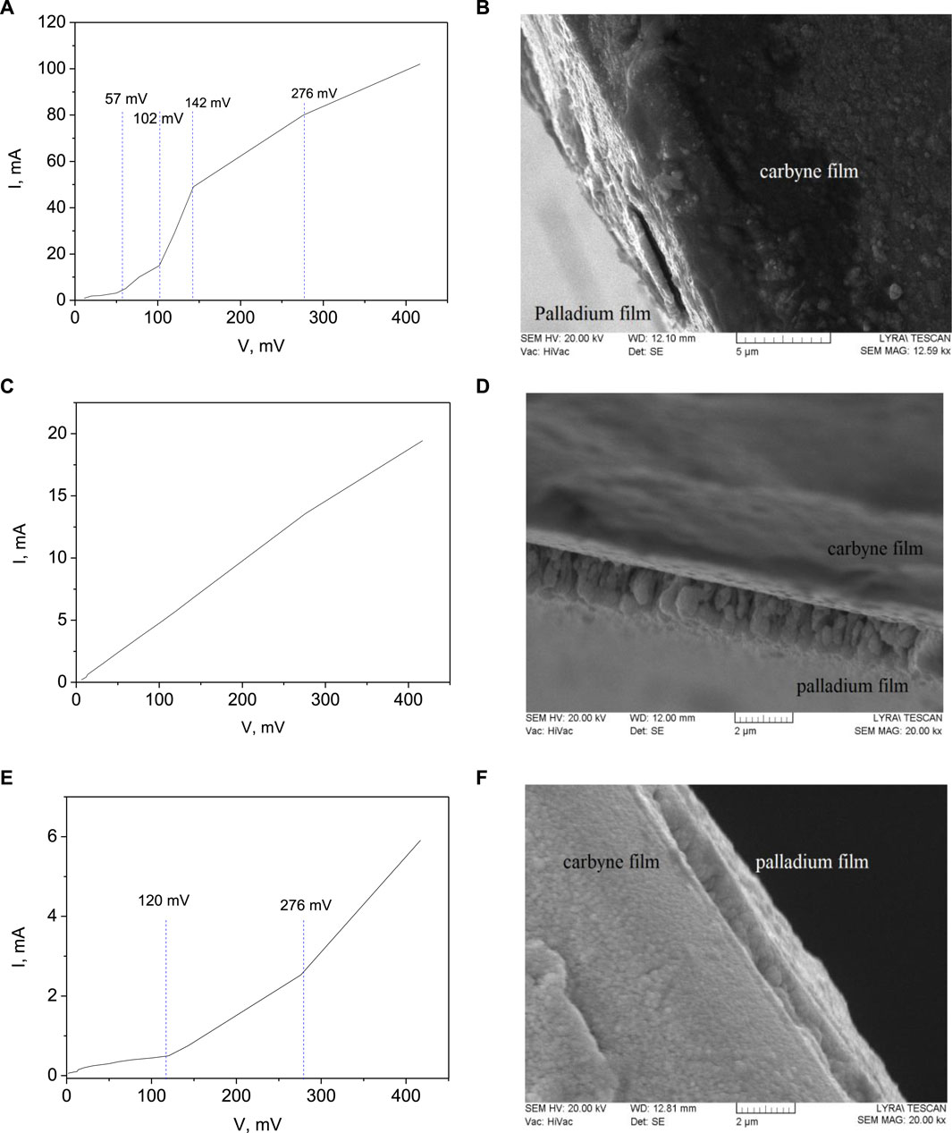
Figure 1. Current-voltage characteristics and SEM images of carbyne-palladium interface for Pd, grown at different sputtering voltages: (A) 0.5 kV; (B) SEM of Pd/carbyne at 0.5 kV; (C) 0.7 kV; (D) SEM of Pd/carbyne at 0.7 kV; (E) 0.9 kV; (F) SEM of Pd/carbyne at 0.9 kV.
The I-V curve with four changes in slope at the lowest sputtering voltage of 0.5 kV suggests a higher density of traps being activated in carbyne (Figure 1A). These traps are likely capturing a significant number of charge carriers, causing frequent alterations in conductivity. At the lowest sputtering voltage, the high number of changes in slope can be attributed to the deposition of Pd coating under conditions that lead to the formation of a rough surface. This irregular surface may introduce numerous defects and trap sites in carbyne, resulting in frequent changes in conductivity. The irregularities are clearly visible from the SEM image, shown in Figure 1B, indicating ∼3.5 µm formations similar to holes, which are probably due to the insufficient energy of the particles, which are not capable to migrate on the surface and get the most favorable energy position reducing the free surface energy. The higher number of changes in slope indicates a more complex trap distribution deeper near the interface and a broad range of energies of trap activation at this voltage range. The material exhibits non-linear behavior due to the increased trapping and detrapping of charge carriers. As traps become saturated at about 150 mV and fewer carriers are captured, the conductivity behavior of the material stabilizes, resulting in less pronounced changes in slope and a more linear relationship between current and voltage. The increasing and then decreasing slopes suggest a dynamic equilibrium between trap activation and carrier capture in the material. The traps in the material, activated by the sputtering process, can also interact with hydrogen molecules after palladium film etching. When hydrogen is introduced to the material, it is expected to be captured by these traps, altering the conductivity and causing changes in the I-V characteristics. Traps can serve as sites where hydrogen molecules can be adsorbed and stored within the material. The presence of traps provides additional binding sites for hydrogen atoms, increasing the overall capacity for hydrogen adsorption. Traps, particularly when distributed uniformly throughout the material, can increase the effective surface area available for hydrogen adsorption. This results in a higher density of hydrogen storage sites and improves the overall storage capacity of the material.
The I-V curve with a linear slope at the intermediate sputtering voltage of 0.7 kV indicates consistent conductivity throughout the measurement range (Figure 1C). This suggests that the traps in carbyne are not as actively capturing charge carriers at this voltage, resulting in a more stable and predictable conductivity. The linear slope suggests a more uniform distribution of traps with a lower density if compared to the case of the surface produced at the lowest sputtering voltage. The material behaves more conventionally in terms of charge transport. The linear slope at the intermediate sputtering voltage suggests also a more uniform and controlled growth of the Pd coating. Under these conditions, the coating forms a smoother and more regular surface, as can be seen in Figure 1D having fewer defects like different grains sizes or orientations.
The I-V curve with only two changes in slope at the highest sputtering voltage of 0.9 kV implies that fewer traps are being activated compared to the lowest voltage (Figure 1E). The conductivity is relatively stable with only moderate deviations in slope. The growth of the Pd coating at this voltage may lead to some localized defects or trap sites in carbyne, causing occasional deviations in conductivity due to striking of highly energetic particles with the carbyne surface. While the growth process at the highest voltage may be more controlled than at the lowest voltage, there can be seen a typical gradient in a stack-type formed layers (Figure 1F). These localized imperfections contribute to the observed changes in conductivity. When sputtering particles have higher energy, they can penetrate deeper into the sublayer (coating surface) and don’t migrates on the surface to find energetically favorable position. This can lead to better mixing of materials, denser film formation, and potentially induce crystallization in the deposited film. Lower-energy sputtering particles may result in a more superficial deposition, which can contribute to the formation of an amorphous or less dense film structure. High-energy sputtering particles results in defects such as vacancies or interstitials in the deposited films and their underlayers.
The thermally stimulated charges (TSC) from the above analyzed samples provide information about the types and concentrations of charge traps present in the material, as well as their energy levels. The interpretation of thermally stimulated charges involves analyzing the temperature-dependent release of trapped charges from a material. By measuring the amount of charge released as a function of temperature (Figure 2), it can be determined the traps nature (shallow or deep). This information can then be used to understand the trapping and recombination processes in the material, as well as to assess the material’s electrical properties and overall performance. As the samples are prepared at different deposition conditions of the top electrode and it was proved with Figure 1 that it affects the current-voltage characteristics and microstructural features, it is expected that the TSC spectra will differ for the three cases. In the context of electronic device’s reliability, traps are considered undesirable because they can capture and immobilize charge carriers, leading to performance degradation, increased power consumption, and potential malfunctions in the device. However, for the purpose of facilitating potential hydrogen release, these traps are beneficial, because they act as sites where hydrogen can be captured, stored, and subsequently released, enabling a more controlled and energy-efficient process for hydrogen storage and release. As the capacity for traps formation is high, as the storage and later releasing ability for the hydrogen isotopes is high. The aim is to control the traps formation for managed release of hydrogen.
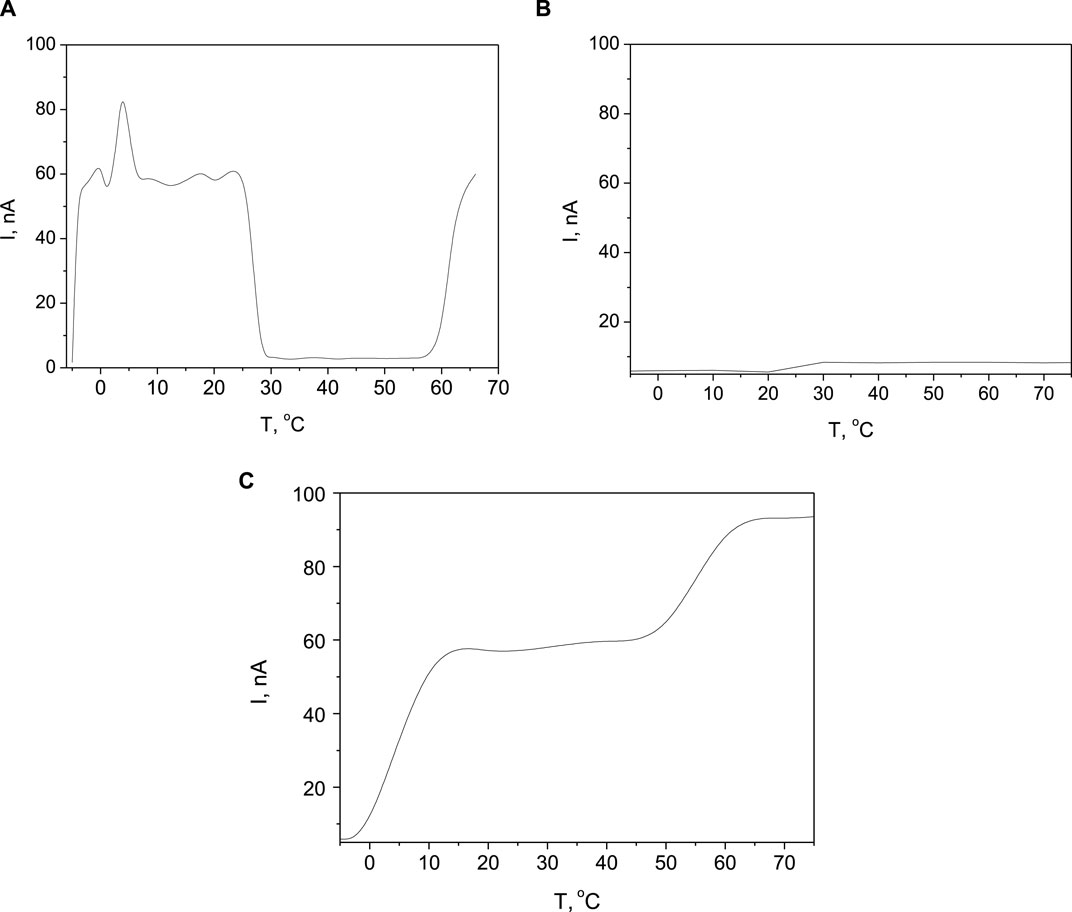
Figure 2. TSC spectra of the samples prepared at sputtering voltage of (A) 0.5 kV; (B) 0.7 kV; (C) 0.9 kV.
Figure 2A shows the TSC spectrum of the sample prepared at sputtering voltage of 0.5 kV. Starting the measurement at a negative temperature can help reset the material to a known starting point before heating it and prevent detrapping at low activation energies. Shallow traps, which are mainly impurities, are defects close to the conduction or valence band, might be more easily ionized at lower temperatures due to the reduced thermal energy available for charge carriers. These traps could contribute to an increase in charge trapping and release processes at negative temperatures, visible at the beginning of the curve below 0°C (at −5°C). The next peak in the current is at 1°C. Interesting is the drop of the TSC current at heating after room temperature, where the current decreased more than 15-fold. Here two scenarios are possible: at higher temperatures, multiple trap states within the material may become active simultaneously. If some traps have higher capture cross-sections or are more energetically favorable for charge trapping, they may dominate the detrapping process, resulting in a net decrease in the TSC current; or certain defects or impurities in the material might undergo migration or reconfiguration at elevated temperatures, changing the distribution of trap states and altering the charge trapping dynamics. This migration can impact the overall TSC behavior and lead to a decrease in current. The next activation of traps was near 60°C, which evidenced for mixed nature of the traps–shallow (activated at low temperatures) and deep (activated at relatively high temperatures). Shallow traps, located near the conduction or valence bands, are often favorable for hydrogen isotope storage and release. The shallow nature of these traps allows for easier capture and release of hydrogen isotopes, making the process more energy efficient and controllable. It should be mentioned that the temperature of the sample can be increased also by intensive light exposure with a specific spectral characteristic, thus providing an avenue for controlling the trapping and release of hydrogen isotopes from external factors.
As was expected from the sample produced at 0.7 kV (Figure 2B), the current formed by thermally stimulated charges is the lowest due to the smallest number of defects releasing captured charge carriers. There is a trend for a constant current flow below 10 nA over the entire studied temperature range. A negligible variation of the conductivity observed around the room temperature confirms that the dominant defects are due to the impurities captured at the grain boundaries (interfaces between regions of different crystallographic orientation).
The thermally stimulated charge spectrum shown in Figure 2C provides critical insights into the behavior of charge carriers within the sample with Pd electrode sputtered at 0.9 kV. The observed behavior in the temperature range of −5 to 0°C, where the current remains small, suggests that at lower temperatures, the thermal energy provided to the system is not sufficient to significantly activate or release charge carriers from their traps. The traps in this context could be impurities within the material that capture charge carriers, preventing them from contributing to the current. As the temperature reaches a certain threshold, evidenced by the sudden three-fold increase in current up to 12°C, it implies that sufficient thermal energy has been provided to activate these traps. The process of thermal activation enables the release of charge carriers that were previously immobilized, thereby contributing to the observed increase in current. The slope of the temperature-dependent behavior is indicative of a relatively narrow distribution but not discrete levels of traps that require a specific range of energy to release the trapped charges, instead of specific amount of energy. The plateau in the current observed up to 50°C may indicate that after the initial release of charge carriers from traps near the lower energy threshold, there are no significant additional traps at energies accessible within this temperature range, leading to a constant current as the rate of trap activation and the recombination of charge carriers reach equilibrium. The subsequent increase in current beyond 50°C, though less pronounced, suggests the presence of traps with higher activation energies. The fact that the increase is not as significant as the first might indicate a lower density of these high-energy traps or considering the smaller slope, it can be suggested a broader distribution of trap energy levels with a continuous supply of thermal energy for gradually activation.
For additional clarification of the defect states nature, Raman measurements were conducted for the carbyne samples after selective wet chemical etching of the top Pd electrodes (Figure 3). The signals measured from the samples with electrodes produced at 0.5 kV and 0.7 kV fully coincide, while the signal, corresponding to sputtering voltage of 0.9 kV exhibits variation of the spectrum, as compared to the lower sputtering voltages. The position and intensities of the bands observed in Raman spectrum are indicative of the bonding state of the carbon atoms. As well, the shape and width of the bands are related either to structural relaxation phenomena or extension of nanocrystalline domains (Ferrari and Robertson, 2001). While for carbyne-enriched film two prominent broad signals located in the ranges 1,000–1,600 and 1,800–2,300 cm−1 should be clearly visible (Compagnini, G. et al., 2005) and can be attributed to the sp2 and sp components, respectively, for the present films the component sp is not visible in any of the samples, despite the sputtering voltage. The peak at 1,072 cm−1 disappears from the Raman spectrum profile for the highest sputtering voltage, indicating structure similar to amorphous carbon. The ratio of the intensities of the main characteristic peaks (1,502 cm−1 and 1,072 cm−1) can be correlated with the presence of boundary defects, such as C–O bonds for low value of this ratio. High value of this ratio that can be achieved when one of the peaks disappears (at sputtering voltage of 0.9 kV) indicate that the defects are mainly due to vacancies (Piedade and Cangueiro, 2020). The peaks below 1,000 cm−1 are not typical for the carbyne and can be due to incorporation of oxygen, resulting in COO− bonds deformation.
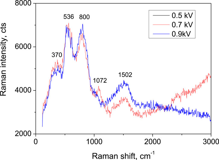
Figure 3. Raman spectroscopy of carbyne films after etching of the Pd electrodes, previously sputtered at voltages of 0.5, 0.7, and 0.9 kV.
This work reports the investigation of the presence of traps when forming contact between Palladium thin films and carbyne material for three different values of the sputtering voltage of the thin films. At different sputtering voltages, the density and distribution of traps vary, leading to different behaviors in the I-V curves. For instance, a higher density of traps is activated at lower sputtering voltages, resulting in more frequent alterations in conductivity. The irregularities in the deposited Pd coating under these conditions introduce numerous defects and trap sites in carbyne, causing nonlinear conductivity behavior. Conversely, at moderate sputtering voltages, the traps are less active, leading to a more stable and linear relationship between current and voltage. The smoother and more regular surface formed under these conditions contributes to more uniform charge transport behavior. At higher sputtering voltages, fewer traps are activated, leading to relatively stable conductivity with occasional deviations. The increased energy of sputtering particles at this voltage can induce localized defects in the material, affecting conductivity. Additionally, thermally stimulated charge (TSC) measurements provide insights into the types and concentrations of traps present in the material, as well as their energy levels. The TSC spectra vary depending on the deposition conditions, with different activation energies for charge traps observed at different temperatures. The behavior of traps at varying temperatures influences the conductivity of the material, with implications for potential hydrogen storage applications.
In summary, the conductivity behavior of carbyne with a palladium interface is intricately linked to trap activation, surface irregularities, and sputtering conditions, highlighting the importance of controlling trap formation for tailored electrical and hydrogen storage properties. Future work will be related to experiments with hydrogen absorption and evaluation of the absorption capacity and retention ability and multiple adsorption/release cycles.
The raw data supporting the conclusions of this article will be made available by the authors, without undue reservation.
MA: Conceptualization, Data curation, Formal Analysis, Funding acquisition, Investigation, Methodology, Project administration, Resources, Software, Supervision, Validation, Visualization, Writing–original draft, Writing–review and editing.
The author(s) declare that financial support was received for the research, authorship, and/or publication of this article. The research was funded by ERA.NET RUS + program, project grant KP-06-DO02/2 CarbyneSense. The author would like to thank the Research and Development Sector at the Technical University of Sofia for the financial support.
The author acknowledges Dr. Bozhidar Stefanov from the Dept. of Chemistry at the Technical University of Sofia for the Raman measurements.
The author declares that the research was conducted in the absence of any commercial or financial relationships that could be construed as a potential conflict of interest.
All claims expressed in this article are solely those of the authors and do not necessarily represent those of their affiliated organizations, or those of the publisher, the editors and the reviewers. Any product that may be evaluated in this article, or claim that may be made by its manufacturer, is not guaranteed or endorsed by the publisher.
Aleksandrova, M., Nikolov, N., and Pandiev, I. (2011). Thermo-stimulation of charges by peltier element for trap analysis in polymer layers. Int. J. Polym. Anal. Ch. 16, 221–227. doi:10.1080/1023666x.2011.569170
Anikina, E., Banerjee, A., Beskachko, V., and Ahuja, R. (2020). Li-decorated carbyne for hydrogen storage: charge induced polarization and van't Hoff hydrogen desorption temperature. Sustain. Energy Fuels 4, 691–699. doi:10.1039/c9se00706g
Checchetto, R., Bazzanella, N., Patton, B., and Miotello, A. (2004). Palladium membranes prepared by r.f. magnetron sputtering for hydrogen purification. Surf. Coat. Technol. 177, 73–79. doi:10.1016/j.surfcoat.2003.06.001
Compagnini, G., Battiato, S., Puglisi, O., Baratta, G. A., and Strazzulla, G. (2005). Ion irradiation of sp rich amorphous carbon thin films: a vibrational spectroscopy investigation. Carbon 43, 3025–3028. doi:10.1016/j.carbon.2005.06.025
Ferrari, A. C., and Robertson, J. (2001). Resonant Raman spectroscopy of disordered, amorphous, and diamond-like carbon. Phys. Rev. B 64, 075414. doi:10.1103/physrevb.64.075414
Kucherik, A., Antipov, A., Kutrovskaya, S., Osipov, A., Povolotckaia, A., and Arakelian, S. (2018). Metal-carbyne clusters for SERS realization. J. Phys. Conf. Ser. 951, 012020. doi:10.1088/1742-6596/951/1/012020
Liu, H., Yang, Y., Xing, M., and Fan, Q. (2024). Two-dimensional carbon allotrope with remarkable electron mobility and tunable band gap under uniaxial strain engineering. Res. Phys. 58, 107435. doi:10.1016/j.rinp.2024.107435
Miao, Z., Ge, Z., Gu, D., Wang, L., and Zhang, T. (2024). Space charge limited current in organic materials with free and trapped charges. Phys.Lett. A 495, 129305. doi:10.1016/j.physleta.2023.129305
Piedade, A. P., and Cangueiro, L. (2020). Influence of carbyne content on the mechanical performance of nanothick amorphous carbon coatings. Nanomaterials 10, 780–799. doi:10.3390/nano10040780
Teyssedre, G., Mendoza-Lopez, D., Laurent, C., Boudou, L., Berquez, L., and Zheng, F. (2021). “Charge trap spectroscopies in polymer dielectrics: application to BOPP,” in 3rd International Conference on High Voltage Engineering and Power Systems (ICHVEPS), October 2021 (Indonesia: Bandung), 57–64.
Tomov, R., and Aleksandrova, M. (2023). “Palladium films as electrodes on carbyne-based devices,” in IEEE 33rd International Conference on Microelectronics, MIEL, Nish, Serbia, October, 2023.
Keywords: carbyne, palladium electrodes, energy release, traps states, nanocoatings
Citation: Aleksandrova M (2024) Investigating the role of palladium electrical contacts in interactions with carbyne nanomaterial solid matter. Front. Mater. 11:1422398. doi: 10.3389/fmats.2024.1422398
Received: 23 April 2024; Accepted: 18 June 2024;
Published: 08 July 2024.
Edited by:
Dimiter Alexandrov, Lakehead University, CanadaReviewed by:
Marc Cahay, University of Cincinnati, United StatesCopyright © 2024 Aleksandrova. This is an open-access article distributed under the terms of the Creative Commons Attribution License (CC BY). The use, distribution or reproduction in other forums is permitted, provided the original author(s) and the copyright owner(s) are credited and that the original publication in this journal is cited, in accordance with accepted academic practice. No use, distribution or reproduction is permitted which does not comply with these terms.
*Correspondence: Mariya Aleksandrova, bV9hbGVrc2FuZHJvdmFAdHUtc29maWEuYmc=
Disclaimer: All claims expressed in this article are solely those of the authors and do not necessarily represent those of their affiliated organizations, or those of the publisher, the editors and the reviewers. Any product that may be evaluated in this article or claim that may be made by its manufacturer is not guaranteed or endorsed by the publisher.
Research integrity at Frontiers
Learn more about the work of our research integrity team to safeguard the quality of each article we publish.