 Davide Cipollini
 Filippo Profumo
 Lambert Schomaker
 Paolo Milani3
 Francesca Borghi
- 1Bernoulli Institute for Mathematics, Computer Science and Artificial Intelligence, University of Groningen, Groningen, Netherlands
- 2CogniGron—Groningen Cognitive Systems and Materials Center, Groningen, Netherlands
- 3CIMAINA—Interdisciplinary Centre for Nanostructured Materials and Interfaces, Department of Physics “Aldo Pontremoli”, University of Milan, Milano, Italy
Nanostructured zirconia and gold films (ns-Au/ZrOx) have been demonstrated as devices characterized by non-linear and hysteretic electrical behavior, with short-term memory and potentiation/depression activity. Here we investigate the conduction mechanisms regulating the non-linear behavior of the nanostructured bilayer Au/ZrOx films. In particular, we investigated the hysteretic I-V curves following the Chua’s approach to memristive systems and separately modelling ion migration and electron transport in the films. The conduction mechanisms exhibited by the bilayered nanostructured system are strongly influenced by the nanogranular morphology that dynamically changes because of electrical stimuli; structural rearrangements are particularly promoted by intense local electric fields and high mobility along bottlenecks and edges in the microstructure. Electron transport is accounted for the Schottky barrier at the electrode interfaces and Poole-Frenkel effect in the bulk nanogranular material, according to a dynamic reorganization of the cluster-assembled network. A model for Poole-Frenkel effect is here discussed to include saturation of the Coulombic traps in the high applied field regime; the proposed model has been validated with experimental voltage ramps with varying sweep-velocity and at different temperatures (from 300 to 200 K), as also by a power exponent parameter analysis.
1 Introduction
A memristor is a two-port passive electronic element whose conductance depends on the history of the applied signal (Chua, 1971). According to the formal description given by (Chua and Kang, 1976), a flux-controlled memristor is a device governed by the two following equations:
where w is the state variable, v is the voltage applied and i is the output current.
After the fabrication of a nanoscale physical memristor by (Strukov et al., 2008), memristive devices have gained increasing attention as they have shown potential predisposition for neuromorphic applications (Mead, 2020) and low power signal processing devices (Christensen et al., 2022). Their synaptic-like behavior is of practical relevance for the emulation of brain computational and learning capabilities in spiking neural networks (Indiveri et al., 2013), as well as to build crossbar arrays for energy efficient hardware for computing steps in artificial intelligence algorithms (Wang et al., 2019; Xia and Yang, 2019).
In literature, memristive systems are most often composed by an insulator thin layer sandwiched between two metal electrodes. To describe the electrical behavior of these devices multiple models are available in the literature, e.g., (Pickett et al., 2009; Laiho et al., 2010; Chang et al., 2011; Yakopcic et al., 2013). We refer to (Linn et al., 2014) for an exhaustive discussion on the applicability of well-established memristive models to describe the complex nonlinear dynamical behavior of such devices.
Fabrication of planar memristors has also been reported. Even though these systems are less represented in the literature, they offer unique opportunities for complex signal information processing applications and for interfaces with biological systems (Fu et al., 2020; Liu et al., 2020). In fact, the planar geometry allows the multi-electrode set up which is a major deviation from the classical two-terminal device paradigm. Thus, a bottom-up self-assembled memristive network connects the electrodes without any top-down construction required for crossbar arrays. In other words, the electrodes take the role of “neurons” while the substrate takes the role of the recurrent synaptic network connecting the neurons. Moreover, these systems allow a larger number of resistance values than a single memristor and increased tunability of the voltage threshold as consequence of the choice of the input/output electrode configuration in the network.
They also provide hardware substrates for application of computing paradigms involving highly dimensional dynamical systems, e.g., reservoir computing (Jaeger, 2001) or echo state networks (Maass et al., 2002), and the collective properties of associative memory, e.g., in Hopfield networks (Hopfield, 1982) and Boltzmann machines (Hinton and Brown, 1999). In the high-dimensional computing paradigm, a key role is played by the large number of elements involved in the computation, enabling higher resistance to noise and fault-tolerant computation capabilities similar to what happens in the brain.
Among a large number of metal oxides used for memristor fabrication, ZrO2 received considerable attention owing to its belonging to high-k dielectrics with high permittivity, simple composition, easy fabrication, and its compatibility with standard CMOS fabrication processes (Sun et al., 2009; Parreira et al., 2016). Recently, sandwiched devices with yttria-stabilized zirconia (YSZ) active layers, exhibiting bipolar resistive switching, have been proposed and regarded as filamentary switching (Gorshkov et al., 2016). They utilized Conductive Atomic Force Microscopy (CAFM) to induce single filament formation in thin YSZ layers, also exploiting Au islands in an underlying layer (Filatov et al., 2017), or Au NPs (Filatov et al., 2018) to concentrate the electric field. Other studies developed a model for device behavior based on oxygen vacancies redistribution (Guseinov et al., 2017). Further electrical characterization techniques revealed insights into ions migration and resistive switching activity (Tikhov et al., 2018; Ryabova et al., 2022), while also demonstrating multi-level device capabilities and neuromorphic behavior akin to Spike Timing-Dependent Plasticity (STDP) (Emelyanov et al., 2019).
In alternative to top-down fabrication approaches, bottom-up self-assembling of nano-objects such as nanowires, nanoparticles and domain walls is gaining increasing attention for the fabrication of neuromorphic devices for different applications (Bose et al., 2017; Mirigliano and Milani, 2021; Zhu et al., 2021; Milano et al., 2022; Rieck et al., 2023; Cipollini et al., 2024). Recently a planar resistive switching system based on nanostructured Au/ZrOx showing short-term plasticity and with structural characteristics compatible with the conditions of in vitro cell culture has been reported (Profumo et al., 2023). The system consists of the superposition of two layers: the bottom one made of a cluster-assembled gold film and the top one of a cluster-assembled zirconia film. Nanostructured zirconia films have interesting biocompatible properties (Schulte et al., 2016; 2018; Previdi et al., 2023) which make them suitable as biological/artificial interface. The non-ohmic and resistive switching behavior of gold cluster-assembled films (CAFs), due to the reorganization of grain boundaries and defects at the interfaces of the nanogranular films (Casu et al., 2024), has been reported also in (Mirigliano et al., 2019; Nadalini et al., 2023); by coupling gold with zirconia CAFs, it is possible to obtain a system exhibiting additional neuromorphic properties such as short-time retention (order of seconds) with stretched-exponential relaxation, and potentiation/depotentiation (Profumo et al., 2023).
Here we investigate the conduction mechanisms of the bilayered nanostructured Au/ZrOx films and we propose a memristive-like model to describe the hysteresis properties of this system: given the large size of the device (4 mm conductive path length) and the large dynamical range of voltage input signal, previously mentioned models for memristors are not able to outline the physical conduction mechanisms since bulk conduction has an important role in this case. We thus develop a model that integrates an ideal bulk-limited and electrode-limited conduction mechanisms. The former addresses conduction in the low resistance state by a modern model of Poole-Frenkel (PF) effect, promoted by the grain boundaries and granularity of the material (Felix et al., 2011). Electrode limited conduction by the Schottky effect is used for the high-resistance state. Finally, an analysis of the power exponent parameter
2 Materials and methods
2.1 Nanostructure fabrication
Ns-Au/ZrOx bilayer films are deposited on a commercial glass coverslip (Zeus 2 cm × 2 cm x 1 mm) cleaned in an ethanol ultrasonic bath for 15 min. The two gold electrodes have been deposited by thermal evaporation and they are separated by a 4 mm long gap. Electrode’s dimensions are 3 mm × 7 mm x 80 nm. A 30 nm thick gold nanostructured film (ns-Au) is deposited using a Supersonic Cluster Beam Deposition (SCBD) apparatus (Milani and Iannotta, 1999; Borghi et al., 2022), filling the gap between the two electrodes with a strip 1 mm large and 6 mm long. Subsequently, a zirconia (ZrOx) nanostructured film of 90 nm thickness is deposited with the same aforementioned apparatus, on the top of the gold thin film (Borghi et al., 2018). The SCBD apparatus is equipped with a Pulsed Microplasma Cluster Source (PMCS) that allows the production of neutral clusters in the gas phase, as described in detail in (Wegner et al., 2006). For further details about fabrication method, we refer to our previously published paper (Profumo et al., 2023). In Figure 1, an Environmental Scanning Electron Microscopy (ESEM) image of the nanocomposite is displayed, showing the granular and porous structure of the ns-Au/ZrOx thin film.
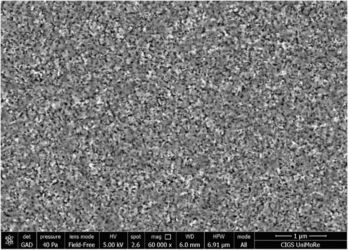
Figure 1. ESEM (ESEM Quanta 200) image of the granular structure of the ns-Au/ZrOx nanocomposite.
2.2 Electrical measurement
The as-deposited layered ns-Au/ZrOx films shows ohmic electrical behavior as previously reported for the single layer of ns-Au film (Mirigliano et al., 2019). After the application of constant voltage higher than roughly 16 V, the device switches to the high resistance state ascribed to the partial breaking and reorganization of the underlying ns-Au film, a so-called forming process, well described for ns-Au film in (Nadalini et al., 2023). Figure 2 shows representative snapshots of the electrical response during the forming process of the non-linear electrical behavior of the bilayered samples: this process is related to a joule heating effect at low voltages A), a non-trivial reorganization of the network at higher voltages due to both heating effects and electroforming mechanisms B) and an abrupt increase in sample resistance at a critical voltage C).
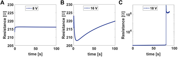
Figure 2. Snapshots of the forming process of the non-linear electrical behavior in bilayered nanostructured sample. (A) Resistance in time at constant voltage 8 V showing initial joule heating effect, (B) resistance at 16 V showing an electrical response driven by the reorganization of the network, (C) resistance at 18 V with an abrupt increase as indicator of an irreversible reorganization of the network.
After the forming process, the device shows a non-linear and hysteretic behavior reported in Figure 3. I-V curves are obtained applying DC voltages starting from −20 V to +20 V with velocity sweep 1V/s and 2.3V/s. The measurements show that for faster voltage sweeps higher currents are obtained. We observe peculiar electrical behaviors consisting in the opening of the curves at non-zero voltage and non-zero current and a saturation effect almost independent of the velocity of the voltage sweep. As first approximation, we discuss in the next Section 2.4 the saturation effect that is ascribable to the saturation of the PF conduction mechanism at a certain critical applied field.
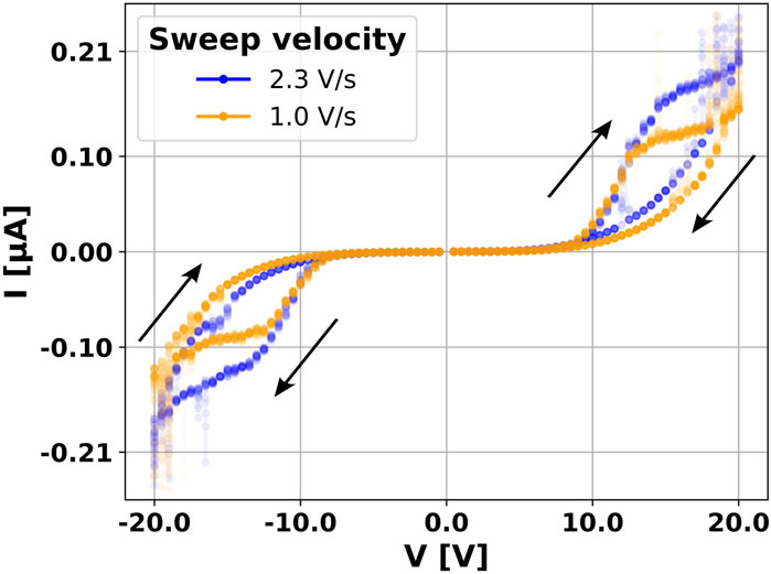
Figure 3. DC I-V sweep for layered Au/ZrOx sample after resistive switching activation. Legend shows voltage sweep velocities. Arrows illustrate the curve path direction.
We verified the stability of the IV curves acquired at the different sweep velocities for ten cycles, as it is reported in Supplementary Material (Supplementary Figure S1). Furthermore, we evaluated the variability of the conduction responses for different devices, nominally identical, i.e., with the same ns-Au and ns- ZrOx thicknesses. In the Supplementary Material (Supplementary Figure S2) the box plots of the main electrical parameters of eight devices (initial resistance before the forming process, resistance after forming process, current value at 20 V and maximum percentual difference between forward and backward currents at fixed voltage) are reported. We noticed the same hysteretic and non-linear behavior, with the highest variability in the current values, principally due to low reproducibility of the contact area between the bilayered nanogranular structure and the bulk electrodes, which affects the current flowing in the devices.
2.3 Electrical measurements at variable temperature
In situ electrical characterization with temperature spanning from ambient temperature (300 K) to 200 K, has been performed in vacuum (p < 10–4 mbar) on films mounted on a copper cold finger of a helium mechanical cryocooler. I-V measurements are performed with a SPD3303X-E Programmable DC Power Supply and an Agilent 34410A multimeter at 2V/s and 1V/s.
2.4 Saturation of the Poole-Frenkel effect
Before describing the memristive-like model developed for our device, we discuss the Poole-Frenkel (PF) effect both in the classical formulation (Frenkel, 1938) and in the modern formulation (Ongaro and Pillonnet, 1989), which incorporates a saturation effect that must be included in a complete model for an emptying-trap process.
The PF effect can be illustrated (see Figure 4A) as the reduction of the potential barrier trapping the electrons to the Coulombic (charged) centers in the bulk material as a consequence of the applied electric field. Consequently, the escape probability of electrons by thermal excitation is increased by the application of the field. In Figure 4A curve a) shows the typical Coulombic potential as a function of the distance from the charged trap. As the electric field is applied, the electron needs smaller energy to escape the attraction of the trap which is reduced by an amount equal to
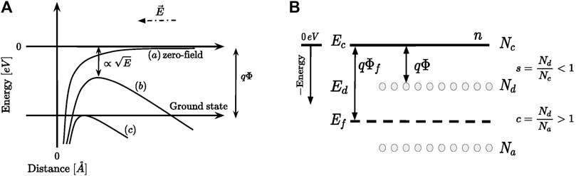
Figure 4. (A) Schematic illustration of the PF effect. The electric field (dashed arrow) lowers the Coulombic potential well. If no field is applied an ionization energy equal to qΦ is required (see curve (a)). Curve (b) illustrates the case of a non-zero electric field applied. Curve (C) shows the saturation effect: for a sufficiently large electric field applied, there is no effective barrier trapping the electron, thus the donor trap centers are ionized. Only the right side of the potential well is depicted. (B) Representative band diagram illustrating the PF effect as described in the original work. The energy levels of the conduction band, Ec, the donor level, Ed, and the Fermi level EF are depicted. The relative position of Ed and EF is arbitrary. Nd and Na indicate the density of donor traps and acceptors. Both panels (A) and (B) are adapted from (Ongaro and Pillonnet, 1989; Harrell and Gopalakrishnan, 2002).
In the classical formulation (Frenkel, 1938), and in its variations available in the literature, the conductivity
where E is the external applied field, K is the Boltzmann constant, T is the temperature,
Thus, the current density J is proportional to:
As firstly recognized in (Ongaro and Pillonnet, 1989), the conductivity,
• The acceptor levels are positioned well-below the Fermi level (see Figure 4B) thus they are completely filled for all values of field and temperature.
• It exists a single donor level at depth
• The density of donor traps is greater than the acceptor density, i.e.,
• The Boltzmann function is used only to describe the statistics of the electrons populating the bottom of the conduction band,
• The Fermi-Dirac function evaluated at the donor energy level describes the probability of occupancy of electrons in the trap’s sites:
The use of the Fermi-Dirac permits the description of the saturation and permits to avoid assumptions on the relative position of the energy levels of
Thanks to the assumption that all acceptors are filled, the equation of conservancy of the charge can be written in the form of
where
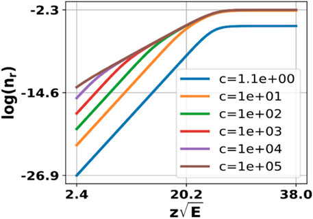
Figure 5. Relative density, nr as a function of the applied field, E, according to Eq. 6. Saturation is observed for
2.5 Bilayered memristive-like model
2.5.1 Electron conduction
To model our system, we consider two elements in parallel as illustrated in the schematic in Figure 6. The geometry of the bilayered network, in which the 30 nm thick ns-Au film is deposited below the 90 nm thick ns-ZrOx film, suggests such a parallel architecture. Furthermore, a similar parallel connection between two electrical components, representing a bulk and an interface conduction mechanisms, is reported in literature for a Schottky in parallel with a SCLC mechanism in (Gomez-Marlasca et al., 2013) and in a simpler fashion by diodes in parallel and series with a interface and bulk resistances respectively in (Acha, 2011). Furthermore, the nanogranular structure of the film promotes local phenomena of ion migration and structural reorganization (Yun et al., 2016) providing a high network responsiveness to the formation of different conductive paths. We are here interested in developing an ideal model describing the main conduction mechanisms, the resistance of the electrodes is hence neglected but they can be implemented in the model with a resistance in series. The first element, depicted as a diode on each interface, as similarly reported in (Gomez-Marlasca et al., 2013) and in (Yang et al., 2008), refers to the electrode-limited conduction which is modelled as Schottky effect according to equation:
where
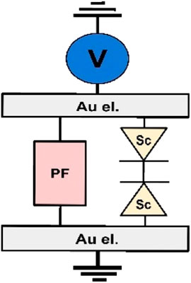
Figure 6. Schematic of the equivalent circuit model for the nanostructured bilayer Au/ZrOx device. See Eq. 9.
The second element represents the PF effect for the bulk conduction. Similarly to what we propose, thin Ba0.8Sr0.2TiO3/ZrO2 heterostructures in a metal-insulator-metal (MIM) configuration resemble Schottky conduction at low electric fields and PF conduction at high ones, probably related to deep trap levels (Sahoo et al., 2013). These two conduction mechanisms have been proposed competing also in the conduction properties of a sputter-deposited Al/ZrO2/Si structure (Chiu et al., 2005) and in the case of thin film metal-insulator-metal capacitors in a unified theory (Lau, 2012). Moreover, the nanostructured gold layer underneath the ZrOx layer enhances the effective field, leading to the saturation of the PF effect for larger voltages applied across the device.
According to this consideration, the standard PF of Eq. 3 is not sufficient to describe the conduction in our device, hence we use the PF equation as proposed by (Ongaro and Pillonnet, 1989). The current density flowing into this element is:
where B is a fitting parameter that takes care of those physical parameters that are not easily accessible from an experimental point of view for an amorphous film as ours, i.e., the density of donor traps, Nc, the mobility of electrons in the low conduction band (or quasi-conduction band for amorphous films),
The total current density flowing into the device is ruled by the following equation:
where
A phenomenon introduced by such nanogranular systems is that grain boundaries and defects promote the formation of barrier layers (Whangbo and Subramanian, 2006; Felix et al., 2011), responsible for dielectric properties of the material which affect both γ and B already mentioned parameters, present in Schottky and Poole-Frenkel mechanisms respectively.
2.5.2 Ion migration
The application of a voltage difference between the electrodes results in the field-driven migration of the ions species through the insulating layer towards the cathode electrode. Ion species might consist of positive ones or oxygen vacancies in the ZrOx layer as similarly reported for the case of (Gomez-Marlasca et al., 2013) and by first-principles calculations in (Shi et al., 2014) as well as metallic ions either injected in the device from the metallic electrodes or from the nanostructured surface of the gold layer below the zirconia layer. The presence of grain boundaries and defects in the nanostructured zirconia layer can favor ion mobility (Yun et al., 2016). Compared to devices made of thin-oxide-film sandwiched between two metals, in our device filament formation spanning the large device size is less likely. The slow ions motion, when compared to the (almost) instantaneous electronic motion, results in a redistribution of charge at the electrode interface which results in a modification of the Schottky barrier at the forced electrode (Yang et al., 2008; Acha, 2011; Gomez-Marlasca et al., 2013), and vice versa for negative applied voltage.
The motion of ions is modelled according to the sinh-model equation from (Chang et al., 2011):
where
3 Results and discussion
3.1 Validation of the bilayered model
To fit the parameters of our model, we used the experimental data shown in Figure 7B. Simulation results for a complete cycle, −20 to 20 V, are illustrated in Figure 7A. The relevant features of the curves, such as the opening of the hysteresis for both non-zero voltages and currents and the saturation effect, are captured by our model. Figure 7 shows on top-left the current time evolution (red curve) for a triangular voltage signal (green curve) applied. The same dynamics is plotted in the I-V plane in the top-right of the figure. In the second row, the state variable w is plotted in time and against the applied voltage signal. In Figure 7B the experimental data are shown for comparison.
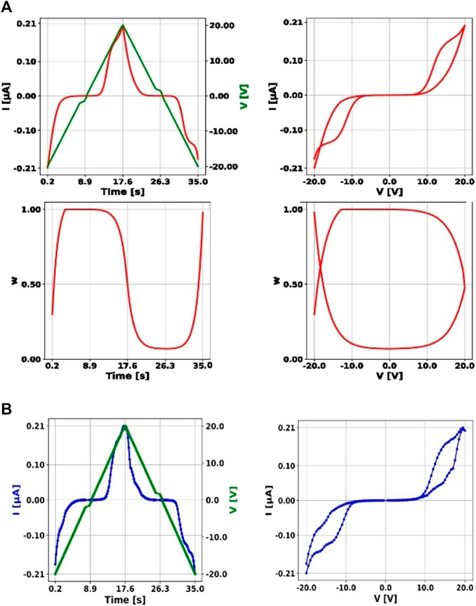
Figure 7. Comparison between our model and measured data. In (A) the simulation of an IV sweep at 2.3 V/s. In the first row, the current and the applied voltage as a function of time are depicted on the left, while on the right the I-V characteristics of the simulated device is shown. On the bottom row, the state-variable is plotted versus time (left) and versus the applied voltage (right). In (B) the experimental data are shown for comparison both in time (left) and in the I-V plane.
Figure 8 shows the simulated I-V curves for two voltage sweep velocities: 2.3 V/s (blue) and 1.0 V/s (orange). Simulation results are in good agreement with experimental measurements (see the experimental I-V characteristic shown in Figure 2) and (Profumo et al., 2023). Furthermore, a good agreement with parameters of (Chiu et al., 2005) is obtained. Fixing T at ambient temperature we obtained a Φp = 0.7 V (1.1 V in (Chiu et al., 2005)) and, given a characteristic length over which the voltage is applied of 200 nm (which is reasonable due to the confinement effect of the Au clusters and corresponding to a medium electric field of 1 MV/cm), a
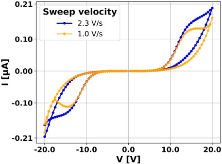
Figure 8. Simulated I-V curve for two sweep velocities.
Limitations of our modelling are believed to be due to the role of second order state variables, as the temperature. In fact, temperature affects both the mobility of ions and the electronic description, thus its role needs to be investigated for future modelling of this device. Furthermore, our modelling does not take into account spontaneous relaxation of the device.
3.2 Experimental IV curves at different temperatures
An analysis from experimental data of the power exponent parameter
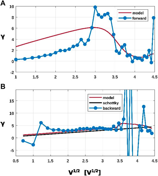
Figure 9. Power exponent parameter G of experimental data (blue dotted lines) and for the model proposed (red lines) as function of
Remarkably, Poole-Frenkel (P-F) emission involves a process similar to Schottky emission, in which thermally excited electrons emit from traps into the dielectric’s conduction band. P-F emission is thus also known as internal Schottky emission (Zafar et al., 1998) and no marked distinction can be made between the bulk- and electrode-limited conduction mechanisms (Chiu, 2014) especially in such a nanogranular structure (Felix et al., 2011). The slower dynamics of ionic migration (when compared to the electrons’ almost-instantaneous dynamics) regulates the switching between the two conduction mechanisms involved, particularly promoted by the network responsiveness.
The low sensitivity of the in-situ apparatus at low current values prevented us from the evaluation of the gamma parameter at lower temperatures. Nevertheless, we reported in Figure 10A representative IV curves acquired at three decreasing temperatures, and on the right (Figure 10B) the Arrhenius plot of the current at 20V, for the backward and forward voltage ramps. These data confirm a hysteretic behavior of the current decreasing at lower temperatures. Furthermore, an exponential fit of the Arrhenius plot stress the accuracy of the proposed model, given the expected temperature dependence of both the Schottky and the Poole-Frenkel mechanisms. For the backward ramp where we propose a main contribute of the Schottky mechanism, a quadratic term in T is included (note that this term has not significant contribute to the fitted curve). The decrease of the hysteresis with temperature can be interpret also with the decreasing mobility of oxygen vacancies in the film (Aleskandrova et al., 2006).
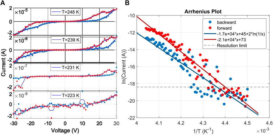
Figure 10. (A) DC I-V sweep for a layered Au/ZrOx samples at different temperatures after resistive switching activation. A continuous line corresponds to a moving average with five points window. Legend shows the mean temperature of each sweep. (B) Arrhenius plot showing the evolution of current at +20 V for a layered Au/ZrOx with the inverse of the temperature. The multimeter resolution limit is reported as a horizontal dashed line. Fit of these data, for forward and backward ramps, are carried out with the Poole-Frenkel and Schottky formula, which give the main contribution in each of these two ramps, respectively.
4 Conclusion
A description of the conduction behavior of a nanostructured bilayer Au/ZrOx film has been proposed as a result of the interplay of a PF and a Schottky mechanisms; on this base a memristive-like model for the devices has been developed. Our model accounts for the electrical hysteretic behavior observed in experimental set-up of a nanogranular network, where ion migration and network reorganization are well promoted. The model is based on ion migration which regulates the relative contribution of two mechanisms of electrical conduction proposed. Electrode-limited conduction is modelled as Schottky effect, while bulk-limited conduction is modelled according to the Poole-Frenkel (PF) effect, where the presence of the two nanogranular materials, full of grain boundaries and defects, promote each of the two mechanisms. In this work we used a refined model for the PF effect which integrates the saturation at high field due to the complete ionization of the traps. Moreover, our model shows good agreement with the experimental data for multiple voltage sweep-velocity as for electrical measurement at different temperatures, as also with power exponent parameter curves.
Both LTSpice and Python code to simulate the memristor are provided (see Supplementary Material).
Data availability statement
The raw data supporting the conclusion of this article will be made available by the authors, without undue reservation.
Author contributions
DC: Writing–original draft, Writing–review and editing, Methodology. FP: Writing–review and editing, Investigation. LS: Writing–review and editing. PM: Writing–review and editing. FB: Writing–review and editing, Investigation.
Funding
The author(s) declare that financial support was received for the research, authorship, and/or publication of this article. This work was partially funded by EUs Horizon 2020, from the MSCA-ITN-2019 Innovative Training Networks program “Materials for Neuromorphic Circuits” (MANIC) under the grant agreement No. 861153. Financial support by the Groningen Cognitive Systems and Materials Center (CogniGron) is gratefully acknowledged. (Corresponding author: DC).
Acknowledgments
We thank Andrea Falqui for the ESEM investigation of the nanostructured nanocomposite sample. We thank Francesco Cavaliere, Licia Pizzo, Giorgio Dall’Oglio and Lorenzo Martinis for providing and operating the cryogenic apparatus used for the low temperature measurements.
Conflict of interest
The authors declare that the research was conducted in the absence of any commercial or financial relationships that could be construed as a potential conflict of interest.
Publisher’s note
All claims expressed in this article are solely those of the authors and do not necessarily represent those of their affiliated organizations, or those of the publisher, the editors and the reviewers. Any product that may be evaluated in this article, or claim that may be made by its manufacturer, is not guaranteed or endorsed by the publisher.
Supplementary material
The Supplementary Material for this article can be found online at: https://www.frontiersin.org/articles/10.3389/fmats.2024.1385792/full#supplementary-material
References
Acha, C. (2011). Dynamical behaviour of the resistive switching in ceramic YBCO/metal interfaces. J. Phys. D Appl. Phys. 44 (34), 345301. doi:10.1088/0022-3727/44/34/345301
Acha, C. (2017). Graphical analysis of current-voltage characteristics in memristive interfaces. J. Appl. Phys. 121 (13), 134502. doi:10.1063/1.4979723
Acha, C., Schulman, A., Boudard, M., Daoudi, K., and Tsuchiya, T. (2016). Transport mechanism through metal-cobaltite interfaces. Appl. Phys. Lett. 109 (1), 011603. doi:10.1063/1.4955204
Aleskandrova, P. V., Gueorguiev, V. K., Ivanov, Tz. E., and Koprinarova, J. B. (2006). Poole-Frenkel conduction in Al/ZrO2/SiO2/Si structures. Eur. Phys. J. B - Condens. Matter Complex Syst. 52 (4), 453–457. doi:10.1140/epjb/e2006-00335-2
Borghi, F., Mirigliano, M., Dellasega, D., and Milani, P. (2022). Influence of the nanostructure on the electric transport properties of resistive switching cluster-assembled gold films. Appl. Surf. Sci. 582, 152485. doi:10.1016/j.apsusc.2022.152485
Borghi, F., Podestà, A., Piazzoni, C., and Milani, P. (2018). Growth mechanism of cluster-assembled surfaces: from submonolayer to thin-film regime. Phys. Rev. Appl. 9 (4), 044016. doi:10.1103/PhysRevApplied.9.044016
Bose, S. K., Mallinson, J. B., Gazoni, R. M., and Brown, S. A. (2017). Stable self-assembled atomic-switch networks for neuromorphic applications. IEEE Trans. Electron Devices 64 (12), 5194–5201. doi:10.1109/TED.2017.2766063
Casu, A., Chiodoni, A., Ivanov, Y. P., Divitini, G., Milani, P., and Falqui, A. (2024). In situ TEM investigation of thermally induced modifications of cluster-assembled gold films undergoing resistive switching: implications for nanostructured neuromorphic devices. ACS Appl. Nano Mater. 7 (7), 7203–7212. doi:10.1021/acsanm.3c06261
Chang, T., Jo, S.-H., Kim, K.-H., Sheridan, P., Gaba, S., and Lu, W. (2011). Synaptic behaviors and modeling of a metal oxide memristive device. Appl. Phys. A 102 (4), 857–863. doi:10.1007/s00339-011-6296-1
Chiu, F.-C. (2014). A review on conduction mechanisms in dielectric films. Adv. Mater. Sci. Eng. 2014, 1–18. doi:10.1155/2014/578168
Chiu, F.-C., Lin, Z.-H., Chang, C.-W., Wang, C.-C., Chuang, K.-F., Huang, C.-Y., et al. (2005). Electron conduction mechanism and band diagram of sputter-deposited Al∕ZrO2∕Si structure. J. Appl. Phys. 97 (3), 034506. doi:10.1063/1.1846131
Christensen, D. V., Dittmann, R., Linares-Barranco, B., Sebastian, A., Gallo, M. L., Redaelli, A., et al. (2022). 2022 roadmap on neuromorphic computing and engineering. Neuromorphic Comput. Eng. 2 (2), 022501. doi:10.1088/2634-4386/ac4a83
Chua, L. O. (1971). “Metristor-The missing circuit element,” in IEEE Transactions on Circuit Theory 18 (5), 507–519. doi:10.1109/TCT.1971.1083337
Chua, L. O., and Kang, S. M. (1976). Memristive devices and systems. Proc. IEEE 64 (2), 209–223. doi:10.1109/PROC.1976.10092
Cipollini, D., Swierstra, A., and Schomaker, L. (2024). Modeling a domain wall network in BiFeO3 with stochastic geometry and entropy-based similarity measure. Front. Mater. 11. doi:10.3389/fmats.2024.1323153
Emelyanov, A. V., Nikiruy, K. E., Demin, V. A., Rylkov, V. V., Belov, A. I., Korolev, D. S., et al. (2019). Yttria-stabilized zirconia cross-point memristive devices for neuromorphic applications. Microelectron. Eng. 215, 110988. doi:10.1016/j.mee.2019.110988
Felix, A. A., Orlandi, M. O., and Varela, J. A. (2011). Schottky-type grain boundaries in CCTO ceramics. Solid State Commun. 151 (19), 1377–1381. doi:10.1016/j.ssc.2011.06.012
Filatov, D., Antonov, D., Antonov, I., Kasatkin, A., and Gorshkov, O. (2017). Resistive switching in stabilized zirconia films studied by conductive atomic Force microscopy. J. Mater. Sci. Chem. Eng. 05 (01), 8–14. doi:10.4236/msce.2017.51002
Filatov, D., Kazantseva, I., Antonov, D., Antonov, I., Shenina, M., Pavlov, D., et al. (2018). Conductive atomic Force microscopy study of the resistive switching in yttria-stabilized zirconia films with Au nanoparticles. Scanning 2018, 1–9. doi:10.1155/2018/5489596
Frenkel, J. (1938). On pre-breakdown phenomena in insulators and electronic semi-conductors. Phys. Rev. 54 (8), 647–648. doi:10.1103/PhysRev.54.647
Fu, T., Liu, X., Gao, H., Ward, J. E., Liu, X., Yin, B., et al. (2020). Bioinspired bio-voltage memristors. Nat. Commun. 11 (1), 1861. Articolo 1. doi:10.1038/s41467-020-15759-y
Gomez-Marlasca, F., Ghenzi, N., Leyva, A. G., Albornoz, C., Rubi, D., Stoliar, P., et al. (2013). Modeling electronic transport mechanisms in metal-manganite memristive interfaces. J. Appl. Phys. 113 (14), 144510. doi:10.1063/1.4800887
Gorshkov, O. N., Mikhaylov, A. N., Kasatkin, A. P., Tikhov, S. V., Filatov, D. O., Pavlov, D. A., et al. (2016). Resistive switching in the Au/Zr/ZrO2-Y2O3/TiN/Ti memristive devices deposited by magnetron sputtering. J. Phys. Conf. Ser. 741 (1), 012174. doi:10.1088/1742-6596/741/1/012174
Guseinov, D. v., Tetelbaum, D. i., Mikhaylov, A. n., Belov, A. i., Shenina, M. e., Korolev, D. s., et al. (2017). Filamentary model of bipolar resistive switching in capacitor-like memristive nanostructures on the basis of yttria-stabilised zirconia. Int. J. Nanotechnol. 14 (7–8), 604–617. doi:10.1504/IJNT.2017.083436
Harrell, W. R., and Gopalakrishnan, C. (2002). Implications of advanced modeling on the observation of Poole–Frenkel effect saturation. Thin Solid Films 405 (1–2), 205–217. doi:10.1016/S0040-6090(01)01752-7
Hill, R. M. (1971). Poole-Frenkel conduction in amorphous solids. Philosophical Mag. A J. Theor. Exp. Appl. Phys. 23 (181), 59–86. doi:10.1080/14786437108216365
Hinton, G. E., and Brown, A. D. (2000). “Spiking Boltzmann machines,” in Advances in Neural Information Processing Systems. Editors A. Solla, T. K. Leen, and K. R. Müller Vol. 12 (Cambridge: MIT Press), 122–128.
Hopfield, J. J. (1982). Neural networks and physical systems with emergent collective computational abilities. Proc. Natl. Acad. Sci. U. S. A. 79 (8), 2554–2558. doi:10.1073/pnas.79.8.2554
Indiveri, G., Linares-Barranco, B., Legenstein, R., Deligeorgis, G., and Prodromakis, T. (2013). Integration of nanoscale memristor synapses in neuromorphic computing architectures. Nanotechnology 24 (38), 384010. doi:10.1088/0957-4484/24/38/384010
Jaeger, H. (2001) The“ echo state” approach to analysing and training recurrent neural networks-with an erratum note’. Bonn, Germany: German National Research Center for Information Technology GMD Technical Report, 148.
Laiho, M., Lehtonen, E., Russell, A., and Dudek, P. (2010). Memristive synapses are becoming reality. Available at: https://www.semanticscholar.org/paper/Memristive-synapses-are- becoming-reality-Laiho-Lehtonen/b8376c268ae11891d21a7297778093dd77ab0953.
Lau, W. S. (2012). An extended unified Schottky-Poole-Frenkel theory to explain the current-voltage characteristics of thin film metal-insulator-metal capacitors with examples for various high-k dielectric materials. ECS J. Solid State Sci. Technol. 1 (6), N139–N148. doi:10.1149/2.006301jss
Linn, E., Siemon, A., Waser, R., and Menzel, S. (2014). Applicability of well-established memristive models for simulations of resistive switching devices. IEEE Trans. Circuits Syst. I Regul. Pap. 61 (8), 2402–2410. doi:10.1109/TCSI.2014.2332261
Liu, Z., Tang, J., Gao, B., Yao, P., Li, X., Liu, D., et al. (2020). Neural signal analysis with memristor arrays towards high-efficiency brain–machine interfaces. Nat. Commun. 11 (1), 4234. Articolo 1. doi:10.1038/s41467-020-18105-4
Maass, W., Natschläger, T., and Markram, H. (2002). Real-time computing without stable states: a new framework for neural computation based on perturbations. Neural Comput. 14 (11), 2531–2560. doi:10.1162/089976602760407955
Mead, C. (2020). How we created neuromorphic engineering. Nat. Electron. 3 (7), 434–435. Articolo 7. doi:10.1038/s41928-020-0448-2
Milani, P., and Iannotta, S. (1999) Cluster Beam synthesis of nanostructured materials. Springer. doi:10.1007/978-3-642-59899-9
Milano, G., Pedretti, G., Montano, K., Ricci, S., Hashemkhani, S., Boarino, L., et al. (2022). In materia reservoir computing with a fully memristive architecture based on self-organizing nanowire networks. Nat. Mater. 21 (2), 195–202. doi:10.1038/s41563-021-01099-9
Mirigliano, M., Borghi, F., Podestà, A., Antidormi, A., Colombo, L., and Milani, P. (2019). Non-ohmic behavior and resistive switching of Au cluster-assembled films beyond the percolation threshold. Nanoscale Adv. 1 (8), 3119–3130. doi:10.1039/C9NA00256A
Mirigliano, M., and Milani, P. (2021). Electrical conduction in nanogranular cluster-assembled metallic films. Adv. Phys. X 6 (1), 1908847. doi:10.1080/23746149.2021.1908847
Nadalini, G., Borghi, F., Košutová, T., Falqui, A., Ludwig, N., and Milani, P. (2023). Engineering the structural and electrical interplay of nanostructured Au resistive switching networks by controlling the forming process. Sci. Rep. 13 (1), 19713. Articolo 1. doi:10.1038/s41598-023-46990-4
Ongaro, R., and Pillonnet, A. (1989). Poole-Frenkel (PF) effect high field saturation. Rev. Phys. Appliquée 24 (12), 1085–1095. doi:10.1051/rphysap:0198900240120108500
Parreira, P., Paterson, G. W., McVitie, S., and MacLaren, D. A. (2016). Stability, bistability and instability of amorphous ZrO 2 resistive memory devices. J. Phys. D Appl. Phys. 49 (9), 095111. doi:10.1088/0022-3727/49/9/095111
Pickett, M. D., Strukov, D. B., Borghetti, J. L., Yang, J. J., Snider, G. S., Stewart, D. R., et al. (2009). Switching dynamics in titanium dioxide memristive devices. J. Appl. Phys. 106 (7), 074508. doi:10.1063/1.3236506
Previdi, A., Borghi, F., Profumo, F., Schulte, C., Piazzoni, C., Lamanna, J., et al. (2023). Nanotopography and microconfinement impact on primary hippocampal astrocyte morphology, cytoskeleton and spontaneous calcium wave signalling. Cells 12 (2), 293. doi:10.3390/cells12020293
Profumo, F., Borghi, F., Falqui, A., and Milani, P. (2023). Potentiation and depression behaviour in a two-terminal memristor based on nanostructured bilayer ZrO x/Au films. J. Phys. D: Appl. Phys. 56 (35), 355301. doi:10.1088/1361-6463/acd704
Rieck, J. L., Cipollini, D., Salverda, M., Quinteros, C. P., Schomaker, L. R. B., and Noheda, B. (2023). Ferroelastic domain walls in BiFeO3 as memristive networks. Adv. Intell. Syst. 5 (1), 2200292. doi:10.1002/aisy.202200292
Ryabova, M. A., Filatov, D. O., Shenina, M. E., Koryazhkina, M. N., Antonov, I. N., Baranova, V. N., et al. (2022). Resonant activation of resistance switching in memristors based on YSZ films with Au nanoparticles. J. Phys. Conf. Ser. 2227 (1), 012020. doi:10.1088/1742-6596/2227/1/012020
Sahoo, S. K., Bakhru, H., Kumar, S., Misra, D., Wolden, C. A., Mohapatra, Y. N., et al. (2013). Field dependent carrier transport mechanisms in metal-insulator–metal devices with Ba0.8Sr0.2TiO3/ZrO2 heterostructured thin films as the dielectric. MRS Online Proc. Libr. 1547 (1), 53–60. doi:10.1557/opl.2013.855
Schulte, C., Lamanna, J., Moro, A. S., Piazzoni, C., Borghi, F., Chighizola, M., et al. (2018). Neuronal cells confinement by micropatterned cluster-assembled dots with mechanotransductive nanotopography. ACS Biomaterials Sci. Eng. 4 (12), 4062–4075. doi:10.1021/acsbiomaterials.8b00916
Schulte, C., Rodighiero, S., Cappelluti, M. A., Puricelli, L., Maffioli, E., Borghi, F., et al. (2016). Conversion of nanoscale topographical information of cluster-assembled zirconia surfaces into mechanotransductive events promotes neuronal differentiation. J. Nanobiotechnology 14 (1), 18. doi:10.1186/s12951-016-0171-3
Shi, L. B., Wang, Y. P., and Li, M. B. (2014). Native defect formation and migration in monoclinic zirconium dioxide. Mater. Sci. Semicond. Process. 27, 586–592. doi:10.1016/j.mssp.2014.07.040
Strukov, D. B., Snider, G. S., Stewart, D. R., and Williams, R. S. (2008). The missing memristor found. Nature 453 (7191), 80–83. Articolo 7191. doi:10.1038/nature06932
Sun, B., Liu, Y. X., Liu, L. F., Xu, N., Wang, Y., Liu, X. Y., et al. (2009). Highly uniform resistive switching characteristics of TiN/ZrO2/Pt memory devices. J. Appl. Phys. 5. doi:10.1063/1.3055414
Tikhov, S., Gorshkov, O., Antonov, I., Morozov, A., Koryazhkina, M., and Filatov, D. (2018). Ion migration polarization in the yttria stabilized zirconia based metal-oxide-metal and metal-oxide-semiconductor stacks for resistive memory. Adv. Condens. Matter Phys. 2018, e2028491–e2028498. doi:10.1155/2018/2028491
Wang, Z., Li, C., Song, W., Rao, M., Belkin, D., Li, Y., et al. (2019). Reinforcement learning with analogue memristor arrays. Nat. Electron. 2 (3), 115–124. Articolo 3. doi:10.1038/s41928-019-0221-6
Wegner, K., Piseri, P., Tafreshi, H. V., and Milani, P. (2006). Cluster beam deposition: a tool for nanoscale science and technology. J. Phys. D Appl. Phys. 39 (22), R439–R459. doi:10.1088/0022-3727/39/22/R02
Whangbo, M.-H., and Subramanian, M. A. (2006). Structural model of planar defects in CaCu3Ti4O12 exhibiting a giant dielectric constant. Chem. Mater. 18 (14), 3257–3260. doi:10.1021/cm060323f
Xia, Q., and Yang, J. J. (2019). Memristive crossbar arrays for brain-inspired computing. Nat. Mater. 18 (4), 309–323. Articolo 4. doi:10.1038/s41563-019-0291-x
Yakopcic, C., Taha, T. M., Subramanyam, G., and Pino, R. E. (2013). Generalized memristive device SPICE model and its application in circuit design. IEEE Trans. Computer-Aided Des. Integr. Circuits Syst. 32 (8), 1201–1214. doi:10.1109/TCAD.2013.2252057
Yang, J. J., Pickett, M. D., Li, X., Ohlberg, D. A. A., Stewart, D. R., and Williams, R. S. (2008). Memristive switching mechanism for metal/oxide/metal nanodevices. Nat. Nanotechnol. 3 (7), 429–433. Articolo 7. doi:10.1038/nnano.2008.160
Yun, J. S., Seidel, J., Kim, J., Soufiani, A. M., Huang, S., Lau, J., et al. (2016). Critical role of grain boundaries for ion migration in formamidinium and methylammonium lead halide perovskite solar cells. Adv. Energy Mater. 6 (13), 1600330. doi:10.1002/aenm.201600330
Zafar, S., Jones, R. E., Jiang, B., White, B., Kaushik, V., and Gillespie, S. (1998). The electronic conduction mechanism in barium strontium titanate thin films. Appl. Phys. Lett. 73 (24), 3533–3535. doi:10.1063/1.122827
Zhou, G., Ren, Z., Sun, B., Wu, J., Zou, Z., Zheng, S., et al. (2020). Capacitive effect: an original of the resistive switching memory. Nano Energy 68, 104386. doi:10.1016/j.nanoen.2019.104386
Keywords: neuromorphic device, resistive switching, nanostructured films, Poole-Frenkel conduction, Schottky interface
Citation: Cipollini D, Profumo F, Schomaker L, Milani P and Borghi F (2024) Conduction mechanisms in a planar nanocomposite resistive switching device based on cluster-assembled Au/ZrOx films. Front. Mater. 11:1385792. doi: 10.3389/fmats.2024.1385792
Received: 13 February 2024; Accepted: 20 May 2024;
Published: 07 June 2024.
Edited by:
Marco Fontana, Polytechnic University of Turin, ItalyReviewed by:
Gianluca Milano, National Institute of Metrological Research (INRiM), ItalyFederico Raffone, Polytechnic University of Turin, Italy
Copyright © 2024 Cipollini, Profumo, Schomaker, Milani and Borghi. This is an open-access article distributed under the terms of the Creative Commons Attribution License (CC BY). The use, distribution or reproduction in other forums is permitted, provided the original author(s) and the copyright owner(s) are credited and that the original publication in this journal is cited, in accordance with accepted academic practice. No use, distribution or reproduction is permitted which does not comply with these terms.
*Correspondence: Davide Cipollini, ZC5jaXBvbGxpbmlAcnVnLm5s; Francesca Borghi, ZnJhbmNlc2NhLmJvcmdoaUB1bmltaS5pdA==
†These authors share first authorship