 Ruben Hamming-Green
 Marcel Van den Broek1
 Laura Bégon-Lours
 Beatriz Noheda
94% of researchers rate our articles as excellent or good
Learn more about the work of our research integrity team to safeguard the quality of each article we publish.
Find out more
ORIGINAL RESEARCH article
Front. Mater., 09 May 2024
Sec. Semiconducting Materials and Devices
Volume 11 - 2024 | https://doi.org/10.3389/fmats.2024.1356610
This article is part of the Research TopicAdvanced Nanomaterials and Devices for Brain-Inspired and Quantum ComputingView all 7 articles
Analog neuromorphic circuits use a range of volatile and non-volatile memristive effects to mimic the functionalities of neurons and synapses. Creating devices with combined effects is important for reducing the footprint and power consumption of neuromorphic circuits. This work presents an epitaxial SmNiO3/BaTiO3 electrical device that displays non-volatile memristive switching to either allow or block access to a volatile threshold switching regime. This behavior arises from coupling the BaTiO3 ferroelectric polarization to SmNiO3 metal–insulator transition; the polarization in the BaTiO3 layer that is in contact with the SmNiO3 layer modifies the device resistance continuously in a controllable, non-volatile manner. Additionally, the polarization state varies the threshold voltage at which the Joule-heating-driven insulator-to-metal phase transition occurs in the nickelate, which results in a negative differential resistance curve and produces a sharp, volatile threshold switch. Reliable current oscillations with stable frequencies, large amplitude, and a relatively low driving voltage are demonstrated when the device is placed in a Pearson–Anson-like circuit.
Negative differential resistance (NDR) is an effect observed in devices made of materials that display strong, non-linear changes in resistivity above an activation threshold (Gibson, 2018). The most popular examples for this effect are materials that undergo temperature-driven transitions from high to low resistances, where the power dissipated during device operation induces the resistance change. In this type of NDR, which is known as the s-type, the NDR regime can be directly observed in current-controlled measurements as a drop in the voltage with increasing current and as threshold switching in voltage-controlled measurements. In contrast, the n-type NDR can be observed as a drop in the current with increasing voltage. Both types of NDRs have been shown to be useful in several ways for neuromorphic circuits, where they can be used as highly compact spike generators (neuristors) (Pickett et al., 2013), selectors (Gibson, 2018), or (coupled) oscillators (Wang et al., 2003; Corti et al., 2018).
Similarly, non-volatile memristive switching has been widely studied for use in neuromorphic applications. The ability of a memristive element to store continuously valued resistance levels endows it with properties that can be used for in-memory computing, such as storing synaptic weights in convolutional networks or as elements in spiking networks that display spike-time-dependent plasticity (Jo et al., 2010; Williams, 2017). Although there are many available memristive materials and mechanisms, ferroelectric materials have been demonstrated as potentially promising candidates as their remanent polarization is multilevel and non-volatile with a fast switching time (Boyn et al., 2017). In two-terminal devices, the polarization can be used to modulate the interfacial or tunneling resistivity or be used as a ferroelectric capacitor (Blom et al., 1994; Chen et al., 2018; Zheng et al., 2019); in a three-terminal device, the polarization can be used as a ferroelectric field-effect transistor (FeFET), where the polarization provides the electric field for modifying the channel resistance (Dutta et al., 2020).
Both threshold and memristive switching have their uses in neuromorphic circuits, and these effects can be linked to provide the necessary behaviors for use in programmable networks or as integrate-and-fire elements, in which the memristive memory integrates the incoming pulses and the threshold switch provides spiking behaviors (Mao et al., 2023). NDR responses in different materials have been shown to be programmable using the field effect in transistor geometry (Dragoman et al., 2008), and this programmability can be used to produce multivalued memory and dynamically reconfigurable logic operations (Sistani et al., 2021). Mixed volatility is generally a desirable property in many proposed neuromorphic circuits as it allows the systems to operate over a wide range of biologically relevant timescales from milliseconds to days (Gerstner et al., 2018). Most of the mixed-volatility devices demonstrated thus far utilize mobile ions that produce different effects at different timescales or voltages, for example, in devices that use both ion migration and filament formation (Ohno et al., 2011; Huang et al., 2016; John et al., 2022).
The typical s-type NDR materials used for spiking or oscillating circuit elements are NbO2 (Kumar et al., 2017) and VO2 (Shukla et al., 2014; Todri-Sanial et al., 2022), which display NDRs when changing from insulating to metallic phases. However, because of the stresses arising from large thermal gradients and structural phase changes at the metal–insulator transitions (MITs), extending the device endurance is difficult and remains a significant challenge in implementing such devices in neuromorphic circuits. Additionally, these materials show considerable device to device variations in their NDR responses (Herzig et al., 2019). More recently, devices using rare earth nickelates (RNiO3; RNOs) (Del Valle et al., 2021; Khandelwal et al., 2023) have been demonstrated; the thin films of these materials are potentially good candidates for NDR elements owing to the tunability of their MIT temperatures as well as subtle crystallographic changes that produce the MITs, which may help greatly extend the endurances of these devices.
RNOs are a class of perovskites in which the MIT temperatures are governed by structural crystallographic phase changes. These materials are unique because of two features. First, the structural change at phase transition occurs via small distortions within the same (perovskite) structure without modifying the chemical coordination. Second, the phase transitions can be tuned over a wide range of temperatures by selecting A-site rare earth elements with different atomic radii (Torrance et al., 1992). In their insulating phases, RNOs are considered as charge-transfer insulators (Zaanen et al., 1985); they are expected to be conducting under the traditional electron band theory, but the electron conduction is inhibited by a strong Coulomb repulsion between the nickel 3d and oxygen p bands. In the insulating phase, the nickel atoms display fully filled d8 orbitals alternating with orbitals that have two d8 ligand holes, resulting in a checkerboard of staggered large and small NiO3 octahedra. As such, the structure in the insulating phase can be viewed as a combination of two different and misaligned sub-lattices with Ni d8 and d8L2 orbital configurations linked by shared oxygen atoms.
Above the transition temperature, in the conductive state, this charge disproportionation disappears and is accompanied by minor shifts in cation positions and octahedral tilts. Owing to the subtle crystallographic shift between these two phases, the MIT temperature can be easily and widely modified via cation substitution, epitaxial strain (Torriss et al., 2017), or injection of oxygen vacancies (Conchon et al., 2007). This has recently been exploited in W/SmNiO3/LSMO devices with large non-volatile memristive windows to produce logic circuits (Li et al., 2023). Similarly, Mott insulator materials have been successfully electrostatically doped by applying electric fields across them (Nakamura et al., 2007); in RNO thin films, this has also been shown to modify the MIT temperatures (Scherwitzl et al., 2010), leading to integration of the RNO thin films with ferroelectrics (Shi et al., 2013; Marshall et al., 2014; Wang et al., 2019). Large (106 factor) non-volatile resistance changes have also been observed in the LaNiO3/BiFeO3 ferroelectric tunnel junctions (Bruno et al., 2016).
The present work demonstrates a system consisting of SmNiO3/BaTiO3/Y-SrSnO3 (SNO/BTO/Y-SSO) stacks grown on Nb:SrTiO3 substrates using pulsed laser deposition (PLD) and displaying both non-volatile memristive and threshold switching behaviors arising from the ferroelectric polarization and nickelate MIT, respectively. Furthermore, while the BaTiO3 in this work appears to be ferroelectric and polarizable, it displays an uncharacteristically high conductivity above the threshold switching voltage. The ferroelectric switching in this case controls the access to the threshold switching regime.
Samarium nickelate (SmNiO3; SNO) was chosen as the MIT material in this work owing to its first-order MIT at TMIT near 125°C (Catalan, 2008), which allows its NDR to be accessed at room temperature. SNO was grown on an insulating LaAlO3 (110) substrate by PLD. The in-plane I-V measurements on two-terminal confined channels (270 μm × 50 μm × 31 nm) produce typical threshold switching/NDR curves (Figure 1A). When placed in a Pearson–Anson-type circuit with a 2 μF parallel capacitor and 1-kΩ series resistor, the current response to DC voltage shows oscillatory characteristics at room temperature (Figure 1B). As Joule heating is responsible for driving the phase change here, the observed threshold voltages are not only derived from material properties and measurement temperature but also largely dependent on the power density, with the smaller channels requiring lower driving voltages. The first-order nature of this transition is a requirement to observe the NDR as the conductivity is dependent on the proportion of metallic to insulating domains. Reducing the thickness of the SNO to under 10 nm diminishes the endurance dramatically, resulting in a device that breaks down after several cycles of switching using an in-plane electric field.
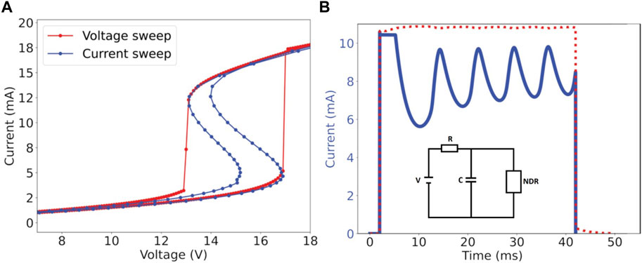
Figure 1. (A) A 30-nm-thick layer of SmNiO3 grown on an insulating LaAlO3 substrate shows negative differential resistance (NDR) when current is driven through a 270-μm-long, 50-μm-wide channel. (B) Joule heating causes a transition from insulating to metallic states. In a voltage-controlled measurement (red), this results in abrupt threshold switching; however, in a current-controlled measurement (blue), the transition from insulator to metal is smooth, resulting in a clear negative slope that typifies s-type NDR. The resistance change is volatile. This device, when coupled to a Pearson–Anson-like circuit (pictured), produces reliable current oscillations under a DC voltage source.
Barium titanate (BaTiO3; BTO) was chosen as the ferroelectric layer and grown on the SrTiO3 (STO) substrate using yttrium-doped SrSnO3 (Y-SSO; 0.075%). This was chosen as the buffer material because of its ability to finely tune the strain in the overlaid BaTiO3 by changing the Y-dopant concentration (Bajpai et al., 2003), which allows the BaTiO3 to be grown with in-plane or out-of-plane polarization orientations. A 90-nm-thick film of BaTiO3 on 20-nm-thick Y-SSO upon UV lithography patterning, contacting Pt electrodes, and performing top-electrode to top-electrode positive-up negative-down (PUND) measurements shows clear switching peaks and high leakage (Figure 2A). The coercive voltages and remanent polarizations observed are typical of compressively strained BaTiO3 thin films (Choi et al., 2004). The relatively large leakage current is also not atypical for thin-film ferroelectrics, which are rarely as insulating or as ideal as their bulk counterparts. While the insulating BTO has a bandgap of 3.4 eV, thin films up to several hundred nanometers thickness are often observed to display n-type semiconducting behaviors and can be highly conductive while still showing ferroelectric responses (Blom et al., 1994; Silva et al., 2017). No NDRs are observed in the BTO/Y-SSO/STO samples without the overlying SNO. Atomic force microscopy of the BTO film depicted in Figure 2A shows excellent surface quality with clearly visible atomic terraces (Figure 2C). The films can also be poled using piezoforce microscopy (PFM), which demonstrates that the films have intrinsic downward out-of-plane polarizations (Figures 2D,E). In Figures 2A,F, the reciprocal space map obtained around the (103) STO peak shows that the BTO growth is oriented with an out-of-plane polarization (long) axis, with the SNO also growing epitaxially.
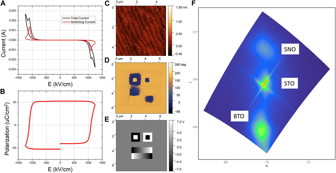
Figure 2. (A) BTO on Y-SSO displays the typical polarizations and switching fields seen in compressively strained BTO thin films (measured in a top-electrode to top-electrode geometry). The films display high leakage currents (black curve) but also have very clear switching peaks, which can be isolated using positive-up negative-down (PUND) measurements (red curve) to produce the P-E loop seen in (B), with a polarization of 50 μC/cm2. Piezoforce microscopy (C–E) shows that the BTO-YSSO films are smooth with visible atomic terraces, can be electrically poled, and have innate polarization in the downward direction. An X-ray diffraction reciprocal space map (F) obtained around the (103) STO diffraction peak shows epitaxially grown and well-oriented out-of-plane BTO and SNO.
Nb(0.5%):SrTiO3 (001) substrates were treated with buffered HF for 40 s and annealed for 80 min at 955°C under O2 flow in a tube furnace. The Y-SSO targets were prepared using standard solid-state synthesis methods as roughly described by Singh et al. (2007) involving vacuum heating precursors (Y2O3, SrCO3, and SnO2), ball milling, annealing at 1,200°C, pressing into a 2 cm pellet under 10 ton of force in the presence of polyvinyl alcohol, and sintering at 1,200°C. A BaTiO3 single crystal and a purchased SmNiO3 pellet were used as the PLD targets. The Y-SSO was grown at 0.3 mbar O2 and 650°C at 1 Hz; the BTO layer was grown at 2 Hz at 0.2 mbar O2 and 620°C, and the SNO was grown at 1 Hz at 0.3 mbar O2 and 600°C. The samples were then annealed at 300 mbar O2 at 600°C for 30 min. The electrodes were deposited using UV-photoresist masks and electron-beam evaporation of 5-nm Ti/70 nm Pt.
Both in-plane and out-of-plane conduction cases were examined in the SNO/BTO/Y-SSO stack grown on Nb:SrTiO3. Circular FET designs were patterned on the SNO surface with circular middle source electrodes that were separated from the outer drain electrodes by a distance of 4 μm (Figure 3B). The substrate was used as the back electrode to simplify device processing and prevent side-wall conduction. Gate voltage pulses were applied to the back electrode in the form of equal and opposite voltages to the source and drain before measuring the channel conductivity. Figure 3A shows that this produces a repeatable change in resistance of about 30% in the SNO channel, with sharp switching voltages and resistance saturation in both the high and low resistance states.
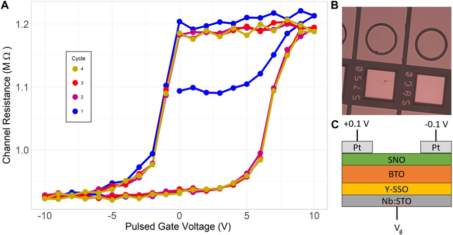
Figure 3. (A): In-plane resistance of SNO on BTO measured at 0.2 V after application of a given gate pulse across the entire stack [in a circular FeFET geometry (B, C)]. The resistance in the SNO channel can be modified by 30% by switching the polarization direction.
Measuring the electrical behavior of the stack from the rectangular top Pt electrodes to the bottom electrode shows that the current response displays both non-volatile and volatile switching components. This was measured through a 100 × 160 μm2 rectangular Pt pad. The four separate regimes of the I-V response at room temperature are colored differently in Figure 4A and will be discussed separately. These are current-controlled measurements, in which the current is gradually increased and decreased, while the voltage supplied is allowed to adapt. The pristine device is in the high-resistance state (HRS). Sweeping with an increasing current and a positive voltage (red curve) performs a non-volatile “Set” action, which abruptly switches the device to the low-resistance state (LRS). This can be observed as a sharp drop in voltage as the current increases. Increasing the current from this point in the LRS tracks an s-type NDR curve, which returns along a similar curve. Subsequent positive current sweeps track the same NDR curve (dark red), and no further non-volatile changes are observed in the response. The volatile threshold switching voltage (where the differential resistance changes sign from positive to negative) shifts from approximately 8 V to 3.5 V, where the precise switching voltage is dependent on the sweep speed that is temperature-driven. The s-type curve displays some stochasticity, which is typical for current-controlled electrical measurements with highly nonlinear responses. Decreasing the temperature to 230 K enhances the NDR in the repeated “Up” curves (Figure 4C) while preserving the non-volatile switching behavior.
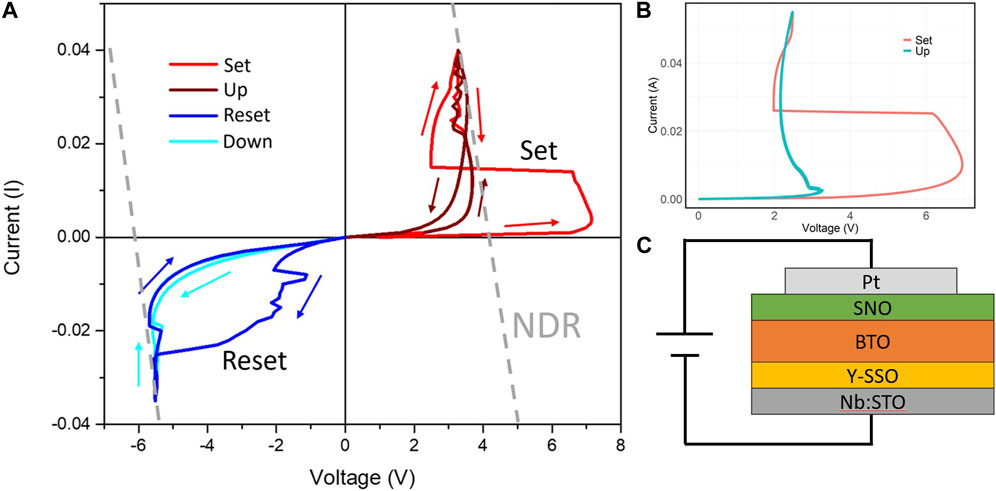
Figure 4. (A) Current-controlled I-V measurements at room temperature in the (C) out-of-plane geometry show large, non-volatile switches in each direction for setting (red) and resetting (blue) the device. After switching, a reliably accessible NDR curve is observed in each direction, providing volatile threshold switching (dark red, light blue). (B) Reducing the temperature to 230 K increases the NDR slope, providing a larger volatile switching window while preserving the non-volatile switching behavior.
When sweeping the current in the negative direction, a “Reset” (dark blue) curve is formed, and the device undergoes non-volatile switching back to the HRS, which then tracks another reliably accessible NDR curve (light blue). After this negative reset, the device is again approximately in the pristine HRS (with the BTO polarization pointing down), and further positive sweeping first follows the “Set” curve, effectively creating a switch for accessing the threshold switch in the positive direction. Similar volatile and non-volatile effects are observed across devices when using identical current-controlled measurement parameters; however, the activation voltages vary from device to device (see Supplementary Material). The volatile NDR threshold position is fairly reliable, with the observed voltages falling within a range of 0.5 V. The non-volatile switching threshold shows more variation, which may be due to either device variability (such as differences in the contact resistance that would modify the power dissipation at a specific voltage and field applied across the bulk of the device) or minor changes in the heating profile arising from the relatively slow feedback control of the current.
The non-volatile switches occur at threshold voltages similar to values where switching is observed in the FeFET geometry measurements (and further matched by the PFM measurements showing intrinsic downward polarization). Conduction at low voltages in the out-of-plane direction appears to be limited by the Poole–Frenkel emission, with comparable values being observed in BaTiO3 on Nb:SrTiO3 (Pan et al., 2012) (see Supplementary Material). Interface-limited conduction mechanisms (Schottky) have been ruled out as the fits are either poor or require non-physical fitting parameters. Importantly, the current is bulk-limited rather than interface-limited, meaning that the electric field gradient is likely over the thickness of the film rather than just across the interface.
To test the robustness of volatile threshold switching, the device was connected in a Pearson–Anson circuit in series with a 100 Ω resistor and in parallel with a variable capacitor. To enhance the NDR and improve the oscillatory behavior, the device was cooled to 230 K. A pulse measurement unit was used to provide 10-m-long pulses at a DC voltage of +3.4 V (Figure 5). At parallel capacitance values below 400 nF, the sharp switching from insulator to metal is accompanied by a period of dampened oscillations before stabilizing in the high-conductivity state. With larger capacitance values, the time to charge the capacitor is enough to let the material cool between each discharge, thereby allowing stable oscillations with stable current maxima and minima across one order of magnitude capacitance range, up to 4,000 nF, with the frequencies ranging from 1.1 to 8.3 kHz. Fast Fourier transform of the current responses display single, sharp dominant frequencies (see Supplementary Material). This oscillating behavior can be switched off by supplying a negative voltage pulse and switching the device to the HRS, where the NDR is no longer accessible with the supplied voltage. When applying simple voltage pulses without attaching parallel capacitors (see Supplementary Material), the volatile switching time decreases logarithmically with the applied voltage and can be switched in a timescale of tens of microseconds.
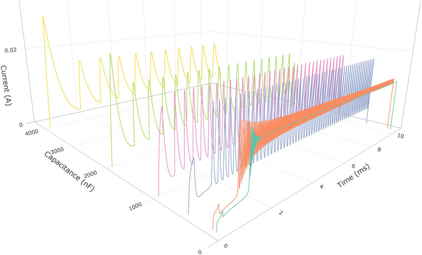
Figure 5. In a Pearson–Anson circuit with a series resistor of 100 Ω, the devices display oscillatory behaviors when placed in parallel with a capacitor and supplied a DC voltage of 3.4 V. When placed in parallel with capacitors exceeding 500 nF, stable peak/valley current values are observed, and the frequencies are dependent on the capacitor charging speeds. For capacitors below 500 nF, the incubation time of the metallic state can be observed clearly as the device heats before experiencing a sharp transition to the metallic state, with dampened current oscillations from the capacitor being observed before stabilizing.
The nature of the non-volatile switch was investigated in the two-terminal out-of-plane geometry. Given the large, abrupt change in resistance that accompanied threshold switching, the non-volatile switching dynamics was explored by applying pulse trains across the device. Because the base current during switching increased as the resistance dropped, a base voltage of 3 V was used, from which pulses of higher magnitudes were applied to monitor the change in resistance with each pulse. To reduce the capacitive effects, the base voltage was chosen to be as high as possible without resulting in any polarization switching. Pulse trains of definite heights and widths were sourced from the top electrode to minimize charging effects. Between each switching measurement, a large negative pulse of −8 V was applied for 1 s to completely reset the device. These trains of pulses produced gradual switching and had a cumulative effect, allowing the response to be finely tuned from the high- to low-resistance state (see Figure 6B). The complete switching speed vs. pulse height is presented in Figure 6A). There is a switching threshold of + 4 V before any non-volatile switching occurs; beyond this value, the switching speed closely follows Merz’s law of domain wall motion, in which the logarithm of the switching time is proportional to 1/V, which is the typical switching behavior of a ferroelectric (Merz, 1954).
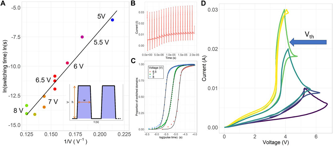
Figure 6. Additional evidence showing that non-volatile switching is ferroelectric in nature despite the large current density through the BTO. Positive pulse trains (B) with fixed heights and widths were applied to a single device until the switching was complete. The time required for complete switching (A) is dependent on the pulse height and can be switched abruptly or smoothly in accordance with Merz’s law of domain wall motion. Additionally, pulses of +4 V and lower do not result in any switching; this non-volatile switching behavior can be reasonably fitted with a nucleation limited switching model (C). The effect of such non-volatile switching on the threshold voltage can be seen in (D), which shows the results of repeated current-controlled measurements with long integration times. As opposed to the pulsed measurements in (A–C), the device is now gradually heated by the applied current, which results in gradual shifting of the threshold switching voltage from approximately 7 V to below 4 V.
Additionally, by measuring the resistance at the base voltage between each pulse (where the heating effects are less pronounced), the evolution of resistance with electrical pulsing can be used to determine the percentage of switched to non-switched BTO. Assuming fully non-switched BTO before the pulse measurements in the HRS (S = 0) and fully switched (S = 1) BTO after the pulse trains are applied as well as assuming that the device resistance between these two boundaries is proportional to the ratio of the switched domains, the switching behavior was analyzed to confirm that it matched with the ferroelectric switching models (Figure 6C). This technique is commonly applied to ferroelectric tunnel junctions to parameterize the switched population ratio (Ma et al., 2020). The Kolmogorov–Avrami–Ishibashi (KAI) model was ruled out as a descriptor of this behavior as the switching observed in this system was less sharp than what would be predicted by this model (Yoshihiro Ishibashi, 1992). However, a reasonably good fit relating S to total pulse time t for a given applied E was found using the nucleation limited switching (NLS) model (Antoniadis et al., 2022) for high pulse-voltage measurements (above 6.5 V). For pulses of lower voltages, which require longer or more pulses, the data no longer fit the NLS model reliably, presumably due to contributions from the volatile switching component because of heating. In summary, the non-volatile switching component agrees with the NLS ferroelectric model and Merz’s law of domain wall motion. Combined with the measurements from BTO without the overlaid SNO layer, which show very clear but leaky switching, this it is strongly evident that the non-volatile component arises from ferroelectric polarization despite being a poor insulator, particularly above the threshold switch.
To exclude the possibility that the switching arises from some other effect, such as oxygen-vacancy migration, a similar film was grown with a different yttrium content in Y-SSO (0.025%) to produce a larger lattice parameter in the buffer layer, thus decreasing the compressive strain on BTO. The BTO grown on this film has an in-plane polarization, as opposed to the out-of-plane polarization in the previously discussed cases. This stack does not show the large non-volatile HRS–LRS switch at all (see Supplementary Material), even while displaying NDR. Conversely, it does display a small non-volatile switch to a slightly higher resistance. This is likely attributable to the oxygen vacancies, which have been well documented to produce memristive switching in both STO and BTO (Jiang et al., 2011; Kessel et al., 2015). This provides further evidence that the switching in the out-of-plane polarized device is in fact due to ferroelectric polarization rather than some other mechanism (such as filamentary- or oxygen-vacancy-based switching).
Lastly, the effect of non-volatile switching on the volatile Vth is shown in Figure 6D. By reducing the current step to 0.1 mA and increasing the measurement integration time in the current-controlled measurements, the interplay of the volatile transition with non-volatile switching can be observed clearly. Upon reaching Vth, the device begins to switch; however, the increased current due to heating prevents the development of large voltages over the non-switched regions. As such, non-volatile switching can also be performed continuously under DC conditions, reducing Vth in each subsequent iteration until switching is complete.
Interfacial effects between these two materials are likely to determine the device behaviors and particularly explain the large changes in resistance through the SNO/BTO stack. The effect of polarization of the ferroelectric layer on RNO has been debated. Jia et al. (2019) investigated the heterostructure formed by the ferroelectric BTO and SNO to present the Au/BTO (20 nm)/SNO device stack. They argued that a two-orders-of-magnitude resistance change is caused by interfacial band bending, where the location of the charge depletion region switches between lying primarily in BTO or in SNO depending on the ferroelectric polarization orientation. Owing to the shifting atomic positions in both materials and charge-transfer-insulator nature of the nickelate, this simple semiconductor band model cannot fully describe the behaviors observed in these systems. At the interface between the ferroelectric perovskite and RNO, a single oxygen atom is bound to the B-site atoms in both ABO3 perovskite materials, to the Ti atom in BTO, and to the Ni atom in SNO. In the bulk BTO, the Ti displacement during full switching is approximately 0.13 Å, while the displacement of the Ni atom between the insulating and metal phases is only approximately 0.05 Å (Zhang et al., 2006; Johnston et al., 2014). Furthermore, charge disproportionation is the primary reason for the insulating state in the charge-transfer-insulator RNO and will be strongly affected by the increased or decreased proportions of electrons in the d8 orbitals of the interfacial nickel, as demonstrated using density functional theory simulations (Malashevich et al., 2018). The three-terminal measurements presented in Figure 3A indicate that the ferroelectric polarization of BTO changes the conductivity of the nickelate layer; this could be due to the resistance change mechanism described here from modification of the Ni orbital structure, electrostatic band bending and charge accumulation, or a combination of the two effects.
The polarization direction has been shown to be able to change the current limiting mechanism in a ferroelectric device (>100 μm thick) from Schottky-like to Ohmic (Blom et al., 1994). Furthermore, while the effect of polarization on the interface may predominantly seem to affect the nickelate, changes in the orbital structures of the electrodes have also been shown to produce dramatically different resistances in ferroelectrics; this was best demonstrated by Pintilie et al., who showed that the interfacial electrode chemistry beyond that which the work function alone would account for could change the apparent ferroelectric responses to result in orders-of-magnitude differences in current densities in otherwise identical samples (Pintilie et al., 2008). Large changes in conduction have been widely reported in ferroelectric semiconductors due to interfacial effects; in the SNO/BTO system, the combination of insulator–metal transition and band bending from ferroelectric polarization would likely give rise to the changes in the conduction behaviors, although further study is necessary to disentangle these effects.
Large non-volatile changes in resistance have been observed in ferroelectric/RNO devices, but the observation of additional volatile threshold switching alongside this non-volatile component has not been reported previously. One reason for this may be that extant works have generally used RNOs with lower MIT temperatures, such that the electrical measurements are obtained while the RNO is in its metallic state. Another reason could be the differences in the ferroelectric layer; the leakiness of BTO is critical for allowing both the threshold switch to occur and its observation. First, the leaky ferroelectric allows a higher current density, resulting in increased Joule heating that causes a phase transition in the SNO. Second, as per Gibson, all materials with temperature-dependent and superlinear increases in conductivity should demonstrate NDRs (Gibson, 2018). If these are not observed experimentally through the electrical measurements, then it does not necessarily imply that there are no parts of the system in which these do not occur. The leakiness of the BTO allows the NDR to be observed externally because it enables a large total change in the current, which would not be otherwise apparent if the BTO was insulating, regardless of the conductivity changes in the SNO. The large leakage currents observed in these devices may seem to counterindicate a ferroelectric switching mechanism behind the non-volatile memory. However, comparisons between the reference BTO samples without the overlaid SNO and in-plane polarized BTO/SNO samples as well as the switching dynamics indicate ferroelectricity despite the large current, which is not necessarily an unprecedented behavior in a ferroelectric thin film. This system has been shown to produce a combination of a non-volatile memristive effect and volatile threshold switching, where the threshold voltage can be modified continuously.
Most examples of mixed-volatility devices use a combination of ion migration and filament formation to achieve multitimescale operation (Ohno et al., 2011; John et al., 2022). The integrate-and-fire functionality, in which the threshold for the current spikes can be controlled, has also been previously reported using oxygen migration (Huang et al., 2016), but this has not been demonstrated in devices operating through the ferroelectric-MIT material combination. Additionally, programmable n-type NDRs have also been shown previously (Sistani et al., 2021), but these have been used as reconfigurable logic elements rather than threshold switching devices (which is more typical of s-type NDRs). A combination of artificial neural networks and spiking neural networks (SNNs) has been suggested as a computational scheme using binary-valued spikes in combination with memristors to allow implementation of gradient descent learning (Zhou et al., 2022). Such devices could also be potentially used in reconfigurable networks, in which the devices can be dynamically reprogrammed to operate as memristors or spiking elements (John et al., 2022). Another proposed model based on combined memristive-spiking devices uses the sparse firing regime, which is an energy-efficient alternative to spiking-rate coding that is often used in SNNs (Bellec et al., 2020), for which such devices may be useful as they could provide non-volatile integration functionality. Furthermore, these devices may be considered in oscillating neural networks that use memristive weights to couple the oscillations of individual elements (Feketa et al., 2021); these devices can also allow oscillators to be dynamically added or removed from a population.
The original contributions presented in the study are publicly available. This data can be found here: https://doi.org/10.34894/62EHA9.
RH-G: conceptualization, investigation, and writing–original draft. MV: investigation and writing–review and editing. LB-L: writing–review and editing. BN: conceptualization and writing–review and editing.
The author(s) declare financial support was received for the research, authorship, and/or publication of this article. The authors would like to acknowledge the financial support of the CogniGron research center and Ubbo Emmius Funds (University of Groningen).
The authors would like to thank Qikai Guo for laboratory supervision of MV and Bert Offrein for the useful discussions and feedback.
The authors declare that the research was conducted in the absence of any commercial or financial relationships that could be construed as a potential conflict of interest.
All claims expressed in this article are solely those of the authors and do not necessarily represent those of their affiliated organizations or those of the publisher, the editors, and the reviewers. Any product that may be evaluated in this article, or claim that may be made by its manufacturer, is not guaranteed or endorsed by the publisher.
The Supplementary Material for this article can be found online at: https://www.frontiersin.org/articles/10.3389/fmats.2024.1356610/full#supplementary-material
Antoniadis, D., Kim, T., and Del Alamo, J. A. (2022). Nucleation-limited switching dynamics model for efficient ferroelectrics circuit simulation. IEEE Trans. Electron Devices 69, 395–399. doi:10.1109/TED.2021.3131290
Bajpai, P. K., Ratre, K., Pastor, M., and Sinha, T. P. (2003). Preparation, characterization and dielectric behaviour of some yttrium doped strontium stannates. Bull. Mater. Sci. 26, 461–464. doi:10.1007/BF02707341
Bellec, G., Scherr, F., Subramoney, A., Hajek, E., Salaj, D., Legenstein, R., et al. (2020). A solution to the learning dilemma for recurrent networks of spiking neurons. Nat. Commun. 11, 3625. doi:10.1038/s41467-020-17236-y
Blom, P. W. M., Wolf, R. M., Cillessen, J. F. M., and Krijn, M. P. C. M. (1994). Ferroelectric Schottky diode. Phys. Rev. Lett. 73, 2107–2110. doi:10.1103/PhysRevLett.73.2107
Boyn, S., Grollier, J., Lecerf, G., Xu, B., Locatelli, N., Fusil, S., et al. (2017). Learning through ferroelectric domain dynamics in solid-state synapses. Nat. Commun. 8, 14736. doi:10.1038/ncomms14736
Bruno, F. Y., Boyn, S., Fusil, S., Girod, S., Carrétéro, C., Marinova, M., et al. (2016). Millionfold resistance change in ferroelectric tunnel junctions based on nickelate electrodes. Adv. Electron. Mater. 2, 1500245. doi:10.1002/aelm.201500245
Catalan, G. (2008). Progress in perovskite nickelate research. Phase Transitions 81, 729–749. doi:10.1080/01411590801992463
Chen, L., Wang, T.-Y., Dai, Y.-W., Cha, M.-Y., Zhu, H., Sun, Q.-Q., et al. (2018). Ultra-low power hf0.5zr0.5o2 based ferroelectric tunnel junction synapses for hardware neural network applications. Nanoscale 10, 15826–15833. doi:10.1039/C8NR04734K
Choi, K. J., Biegalski, M., Li, Y. L., Sharan, A., Schubert, J., Uecker, R., et al. (2004). Enhancement of ferroelectricity in strained BaTiO3 thin films. Science 306, 1005–1009. doi:10.1126/science.1103218
Conchon, F., Boulle, A., Guinebretière, R., Girardot, C., Pignard, S., Kreisel, J., et al. (2007). Effect of tensile and compressive strains on the transport properties of SmNiO3 layers epitaxially grown on (001) SrTiO3 and LaAlO3 substrates. Appl. Phys. Lett. 91, 192110. doi:10.1063/1.2800306
Corti, E., Gotsmann, B., Moselund, K., Stolichnov, I., Ionescu, A., and Karg, S. (2018). “Resistive coupled VO2 oscillators for image recognition,” in 2018 IEEE international conference on rebooting computing (ICRC) (McLean, VA, USA: IEEE), 1–7. doi:10.1109/ICRC.2018.8638626
Del Valle, J., Rocco, R., Domínguez, C., Fowlie, J., Gariglio, S., Rozenberg, M. J., et al. (2021). Dynamics of the electrically induced insulator-to-metal transition in rare-earth nickelates. Phys. Rev. B 104, 165141. doi:10.1103/PhysRevB.104.165141
Dragoman, M., Konstantinidis, G., Kostopoulos, A., Dragoman, D., Neculoiu, D., Buiculescu, R., et al. (2008). Multiple negative resistances in trenched structures bridged with carbon nanotubes. Appl. Phys. Lett. 93, 043117. doi:10.1063/1.2963367
Dutta, S., Schafer, C., Gomez, J., Ni, K., Joshi, S., and Datta, S. (2020). Supervised learning in all fefet-based spiking neural network: opportunities and challenges. Front. Neurosci. 14, 634. doi:10.3389/fnins.2020.00634
Feketa, P., Schaum, A., and Meurer, T. (2021). Synchronization and multicluster capabilities of oscillatory networks with adaptive coupling. IEEE Trans. Automatic Control 66, 3084–3096. doi:10.1109/TAC.2020.3012528
Gerstner, W., Lehmann, M., Liakoni, V., Corneil, D., and Brea, J. (2018). Eligibility traces and plasticity on behavioral time scales: experimental support of neohebbian three-factor learning rules. Front. Neural Circuits 12, 53. doi:10.3389/fncir.2018.00053
Gibson, G. A. (2018). Designing negative differential resistance devices based on self-heating. Adv. Funct. Mater. 28, 1704175. doi:10.1002/adfm.201704175
Herzig, M., Weiher, M., Ascoli, A., Tetzlaff, R., Mikolajick, T., and Slesazeck, S. (2019). Multiple slopes in the negative differential resistance region of nbox-based threshold switches. J. Phys. D Appl. Phys. 52, 325104. doi:10.1088/1361-6463/ab217a
Huang, Y.-J., Chao, S.-C., Lien, D.-H., Wen, C.-Y., He, J.-H., and Lee, S.-C. (2016). Dual-functional memory and threshold resistive switching based on the push-pull mechanism of oxygen ions. Sci. Rep. 6, 23945. doi:10.1038/srep23945
Ishibashi, Y.(1992). Theory of polarization reversals in ferroelectrics based on landau-type free energy. Jpn. J. Appl. Phys. 31, 2822. doi:10.1143/JJAP.31.2822
Jia, M.-X., Ren, Z.-Q., Liu, Y.-D., Cheng, Y., Huang, R., Xiang, P.-H., et al. (2019). Ferroelectric polarization-controlled resistive switching in BaTiO3/SmNiO3 epitaxial heterostructures. Appl. Phys. Lett. 114, 102901. doi:10.1063/1.5066032
Jiang, W., Noman, M., Lu, Y. M., Bain, J. A., Salvador, P. A., and Skowronski, M. (2011). Mobility of oxygen vacancy in SrTiO 3 and its implications for oxygen-migration-based resistance switching. J. Appl. Phys. 110, 034509. doi:10.1063/1.3622623
Jo, S. H., Chang, T., Ebong, I., Bhadviya, B. B., Mazumder, P., and Lu, W. (2010). Nanoscale memristor device as synapse in neuromorphic systems. Nano Lett. 10, 1297–1301. doi:10.1021/nl904092h
John, R. A., Demirağ, Y., Shynkarenko, Y., Berezovska, Y., Ohannessian, N., Payvand, M., et al. (2022). Reconfigurable halide perovskite nanocrystal memristors for neuromorphic computing. Nat. Commun. 13, 2074. doi:10.1038/s41467-022-29727-1
Johnston, S., Mukherjee, A., Elfimov, I., Berciu, M., and Sawatzky, G. A. (2014). Charge disproportionation without charge transfer in the rare-earth-element nickelates as a possible mechanism for the metal-insulator transition. Phys. Rev. Lett. 112, 106404. doi:10.1103/PhysRevLett.112.106404
Kessel, M., De Souza, R. A., and Martin, M. (2015). Oxygen diffusion in single crystal barium titanate. Phys. Chem. Chem. Phys. 17, 12587–12597. doi:10.1039/C5CP01187F
Khandelwal, U., Guo, Q., Noheda, B., Nukala, P., and Chandorkar, S. (2023). Dynamics of voltage-driven self-sustained oscillations in NdNiO3 neuristors. ACS Appl. Electron. Mater. 5, 3859–3864. doi:10.1021/acsaelm.3c00549
Kumar, S., Wang, Z., Davila, N., Kumari, N., Norris, K. J., Huang, X., et al. (2017). Physical origins of current and temperature controlled negative differential resistances in NbO2. Nat. Commun. 8, 658. doi:10.1038/s41467-017-00773-4
Li, L., Yu, D., Wei, Y., Sun, Y., Zhao, J., Zhou, Z., et al. (2023). A SmNiO 3 memristor with artificial synapse function properties and the implementation of Boolean logic circuits. Nanoscale 15, 7105–7114. doi:10.1039/D2NR06044B
Ma, C., Luo, Z., Huang, W., Zhao, L., Chen, Q., Lin, Y., et al. (2020). Sub-nanosecond memristor based on ferroelectric tunnel junction. Nat. Commun. 11, 1439. doi:10.1038/s41467-020-15249-1
Malashevich, A., Marshall, M. S. J., Visani, C., Disa, A. S., Xu, H., Walker, F. J., et al. (2018). Controlling mobility in perovskite oxides by ferroelectric modulation of atomic-scale interface structure. Nano Lett. 18, 573–578. doi:10.1021/acs.nanolett.7b04715
Mao, H., Zhu, Y., Ke, S., Zhu, Y., Shi, K., Wang, X., et al. (2023). A tunable leaky integrate-and-fire neuron based on one neuromorphic transistor and one memristor. Appl. Phys. Lett. 123, 013501. doi:10.1063/5.0151312
Marshall, M. S. J., Malashevich, A., Disa, A. S., Chen, H., Ismail-Beigi, S., Walker, F. J., et al. (2014). “Modulating the properties of thin film nickelates using a ferroelectric,” in APS March Meeting Abstracts. vol. 2014 of APS Meeting Abstracts, D49.006.
Merz, W. J. (1954). Domain Formation and domain wall motions in ferroelectric BaTi O 3 single crystals. Phys. Rev. 95, 690–698. doi:10.1103/PhysRev.95.690
Nakamura, M., Sawa, A., Sato, H., Akoh, H., Kawasaki, M., and Tokura, Y. (2007). Optical probe of electrostatic-doping in an n -type Mott insulator. Phys. Rev. B 75, 155103. doi:10.1103/PhysRevB.75.155103
Ohno, T., Hasegawa, T., Tsuruoka, T., Terabe, K., Gimzewski, J. K., and Aono, M. (2011). Short-term plasticity and long-term potentiation mimicked in single inorganic synapses. Nat. Mater. 10, 591–595. doi:10.1038/nmat3054
Pan, R. K., Zhang, T. J., Wang, J. Z., Ma, Z. J., Wang, J. Y., and Wang, D. F. (2012). Rectifying behavior and transport mechanisms of currents in Pt/BaTiO 3/Nb:SrTiO 3 structure. J. Alloys Compd. 519, 140–143. doi:10.1016/j.jallcom.2011.12.146
Pickett, M. D., Medeiros-Ribeiro, G., and Williams, R. S. (2013). A scalable neuristor built with Mott memristors. Nat. Mater. 12, 114–117. doi:10.1038/nmat3510
Pintilie, L., Vrejoiu, I., Hesse, D., and Alexe, M. (2008). The influence of the top-contact metal on the ferroelectric properties of epitaxial ferroelectric Pb(Zr0.2Ti0.8)O3 thin films. J. Appl. Phys. 104, 114101. doi:10.1063/1.3021293
Scherwitzl, R., Zubko, P., Lezama, I. G., Ono, S., Morpurgo, A. F., Catalan, G., et al. (2010). Electric-field control of the metal-insulator transition in ultrathin NdNiO3 films. Adv. Mater. 22, 5517–5520. doi:10.1002/adma.201003241
Shi, J., Ha, S. D., Zhou, Y., Schoofs, F., and Ramanathan, S. (2013). A correlated nickelate synaptic transistor. Nat. Commun. 4, 2676. doi:10.1038/ncomms3676
Shukla, N., Parihar, A., Freeman, E., Paik, H., Stone, G., Narayanan, V., et al. (2014). Synchronized charge oscillations in correlated electron systems. Sci. Rep. 4, 4964. doi:10.1038/srep04964
Silva, J. P., Faita, F. L., Kamakshi, K., Sekhar, K. C., Moreira, J. A., Almeida, A., et al. (2017). Enhanced resistive switching characteristics in Pt/BaTiO3/ITO structures through insertion of HfO2:Al2O3 (HAO) dielectric thin layer. Sci. Rep. 7, 46350. doi:10.1038/srep46350
Singh, S., Singh, P., Parkash, O., and Kumar, D. (2007). Synthesis, microstructure and electrical properties of Ti doped SrSnO3. Adv. Appl. Ceram. 106, 231–234. doi:10.1179/174367607X202573
Sistani, M., Böckle, R., Falkensteiner, D., Luong, M. A., den Hertog, M. I., Lugstein, A., et al. (2021). Nanometer-scale ge-based adaptable transistors providing programmable negative differential resistance enabling multivalued logic. ACS Nano 15, 18135–18141. doi:10.1021/acsnano.1c06801
Todri-Sanial, A., Carapezzi, S., Delacour, C., Abernot, M., Gil, T., Corti, E., et al. (2022). How frequency injection locking can train oscillatory neural networks to compute in phase. IEEE Trans. Neural Netw. Learn. Syst. 33, 1996–2009. doi:10.1109/TNNLS.2021.3107771
Torrance, J., Lacorre, P., Nazzal, A., Ansaldo, E., and Niedermayer, C. (1992). Systematic study of insulator-metal transitions in perovskites RNiO3 (R=Pr,Nd,Sm,Eu) due to closing of charge-transfer gap. Phys. Rev. B 45, 8209–8212. doi:10.1103/PhysRevB.45.8209
Torriss, B., Margot, J., and Chaker, M. (2017). Metal-insulator transition of strained SmNiO3 thin films: structural, electrical and optical properties. Sci. Rep. 7, 40915. doi:10.1038/srep40915
Wang, J., Wheeler, D., Yan, Y., Zhao, J., Howard, S., and Seabaugh, A. (2003). Silicon tunnel diodes formed by proximity rapid thermal diffusion. Electron Device Lett. IEEE 24, 93–95. doi:10.1109/LED.2002.807706
Wang, X., Wu, M., Wei, F., Zhang, Y., Zheng, C., Lou, X., et al. (2019). Electroresistance of Pt/BaTiO 3/LaNiO 3 ferroelectric tunnel junctions and its dependence on BaTiO 3 thickness. Mater. Res. Express 6, 046307. doi:10.1088/2053-1591/aafae0
Williams, R. S. (2017). What’s next? [the end of moore’s law]. Comput. Sci. Eng. 19, 7–13. doi:10.1109/MCSE.2017.31
Zaanen, J., Sawatzky, G. A., and Allen, J. W. (1985). Band gaps and electronic structure of transition-metal compounds. Phys. Rev. Lett. 55, 418–421. doi:10.1103/PhysRevLett.55.418
Zhang, Q., Cagin, T., and Goddard, W. A. (2006). The ferroelectric and cubic phases in BaTiO3 ferroelectrics are also antiferroelectric. Proc. Natl. Acad. Sci. U. S. A. 103, 14695–14700. doi:10.1073/pnas.0606612103
Zheng, Q., Wang, Z., Gong, N., Yu, Z., Chen, C., Cai, Y., et al. (2019). Artificial neural network based on doped hfo2 ferroelectric capacitors with multilevel characteristics. IEEE Electron Device Lett. 40, 1309–1312. doi:10.1109/LED.2019.2921737
Keywords: ferroelectric, memristor, threshold switching, negative differential resistance, neuromorphic, nickelates, metal–insulator transition, BaTiO3
Citation: Hamming-Green R, Van den Broek M, Bégon-Lours L and Noheda B (2024) Mixed volatility in a single device: memristive non-volatile and threshold switching in SmNiO3/BaTiO3 devices. Front. Mater. 11:1356610. doi: 10.3389/fmats.2024.1356610
Received: 15 December 2023; Accepted: 27 March 2024;
Published: 09 May 2024.
Edited by:
Steven Koester, University of Minnesota Twin Cities, United StatesReviewed by:
Lakshmi Narayanan Mosur Saravana Murthy, Intel, United StatesCopyright © 2024 Hamming-Green, Van den Broek, Bégon-Lours and Noheda. This is an open-access article distributed under the terms of the Creative Commons Attribution License (CC BY). The use, distribution or reproduction in other forums is permitted, provided the original author(s) and the copyright owner(s) are credited and that the original publication in this journal is cited, in accordance with accepted academic practice. No use, distribution or reproduction is permitted which does not comply with these terms.
*Correspondence: Ruben Hamming-Green, ci5wLmhhbW1pbmctZ3JlZW5AcnVnLm5s; Beatriz Noheda, Yi5ub2hlZGFAcnVnLm5s
Disclaimer: All claims expressed in this article are solely those of the authors and do not necessarily represent those of their affiliated organizations, or those of the publisher, the editors and the reviewers. Any product that may be evaluated in this article or claim that may be made by its manufacturer is not guaranteed or endorsed by the publisher.
Research integrity at Frontiers
Learn more about the work of our research integrity team to safeguard the quality of each article we publish.