
94% of researchers rate our articles as excellent or good
Learn more about the work of our research integrity team to safeguard the quality of each article we publish.
Find out more
ORIGINAL RESEARCH article
Front. Mater., 15 February 2024
Sec. Semiconducting Materials and Devices
Volume 11 - 2024 | https://doi.org/10.3389/fmats.2024.1354522
 Beomsu Jo1†
 Kanghoon Seo2†
 Kyumin Park2
 Chaewon Jeong2
 Bathalavaram Poornaprakash1
 Moonsang Lee2
 Singiri Ramu1*
 Myung Gwan Hahm2*
 Young Lae Kim1*
The development of photodetectors is crucial in fields such as optical communication, image sensing, medical devices and military equipment, where high sensitivity is paramount. We fabricated an ambipolar photodiode using monolayer triclinic ReSe2, synthesized by chemical vapor deposition on p-type Si substrate. The photodetector has a broadband response range from 405 to 1100 nm. The device exhibits high sensitivity to NIR radiation with a high Iph/Idark (ON/OFF) ratio of 5.8 × 10⁴, responsivity (R) of 465 A/W, and specific detectivity (D) of 4.8 × 10¹³ Jones at open circuit voltage (Voc), indicating photovoltaic behavior. Our ReSe2/Si heterojunction photodetector also exhibits low dark current of 1.4 × 10⁻⁹ A and high external quantum efficiency (EQE) of 54368.2% for 1060 nm at -3 V, demonstrating a photoconductive gain. The maximum responsivity (R = 465 A/W) can be achieved at -3 V reverse bias under 1060 nm. The device has a high ideality factor (4.8) and power coefficient (α = 0.5), indicating the presence of interface and sub-gap states that enhance device responsivity at lower illumination intensities by re-exciting trapped carriers into the conduction band. Our results offer important insights into the underlying photo-physics of the ReSe2/Si heterojunction and propose promising avenues for developing advanced broadband photodetectors of high performance.
Photodetectors are essential devices that can detect photons and convert them into electrical signals making them widely used in various fields such as Artificial Silicon Retina (Retinal Prosthesis–MEMS), telecommunications, image sensors, biomedicine, military surveillance, and security equipment (Chenais et al., 2021; Yu et al., 2016; García-Hemme et al., 2014; Dong et al., 2014; Sun et al., 2017; Rogalski, 2002; Yan et al., 2017a). Photodetectors are characterized by several stringent requirements for optimum functioning, including spectral response, photosensitivity, low dark current, low noise equivalent power, high quantum efficiency, and fast timing response (rise time and fall time) (Supplementary Figure S1) at their working wavelength range (Gupta and Kumar, 2022; Shelke et al., 2020). The distinct properties of silicon, such as a large absorption coefficient at near-infrared, low cost, and excellent compatibility, have attracted the research community to develop Si-based photodetectors (WX2/Si, MoX2/Si where X = S, Se) (Sun et al., 2018; Hasani et al., 2019). Rhenium-based transition metal dichalcogenides (TMDCs) have also generated interest due to their unique in-plane anisotropic optoelectronic properties (Liu et al., 2015; Jariwala et al., 2016a; Hart et al., 2016; Hart et al., 2016; Arora et al., 2017). ReSe2 has a stable distorted 1T phase with layer-independent indirect band structure in the range of 0.9–1.3 eV from bulk to monolayer (Arora et al., 2017; Jiang et al., 2018; Li et al., 2020). Therefore, the ReSe2/Si system is an ideal candidate for the fabrication of high-performance broadband photodetectors. However, the responsivity of ReSe2 (Zhu et al., 2021) and Si (Haynes and Hornbeck, 1953) semiconductors suffer from intrinsic defect states in the forbidden zone at higher illumination intensities. We report a highly sensitive and chemical vapor deposition (CVD)-grown ReSe2/Si photodetector with trap-assisted photoresponsivity at lower illumination intensities. The high ideality factor (4.8) and power coefficient (α = 0.5) reveal defect and trap states. The heterojunction photodiode has conductive gain at −3 V under NIR radiation (1,060 nm) with good reproducibility. The responsivity, specific detectivity, and EQE are evaluated to be 465 A/W, 1.4 × 10¹³ Jones, and 54368.2%, respectively. The heterojunction photodetector exhibits broadband spectral selectivity with a peak response at 1,060 nm. The generalization of the above result proves that this ReSe2/Si sensor will have potential application in future ultra-sensitive photodetectors.
High-quality pristine monolayer ReSe2 was synthesized using a CVD method as shown in Figure 1A. Monolayer ReSe2 was synthesized on SiO2/Si half-etched wafer (1 cm × 1 cm) via Chemical Vapor Deposition (CVD) method. Rhenium (Ⅵ) Oxide (ReO3) and Selenium (Se) Powder was used as precursor. And Sodium Chloride (NaCl) was used to boost the synthesis reaction. Prepare the cleaned SiO2/Si wafer with Acetone-Isopropyl alcohol (IPA) - Deionized water using ultrasonication and dry the wafer using nitrogen (N2) gas. Put 20 mg ReO3 2 cm away from the head of the alumina (Al2O3) boat as a Rhenium precursor. And 1.5 mg NaCl 1 cm away from the head of the boat to boost the reaction. Place the wafer SiO2 side facing down on the boat and put Selenium powder in another alumina boat. Place the Rhenium boat and Selenium boat at 600°C and 400°C sites each and purge the furnace for 10 min with 150 sccm 15% H2-Ar mixture gas. After purging step, furnace was heated-up to 600°C at a rate of 25°C/min and reacted for 20 min at target temperature with same flow rate. And when the reaction is over, Cool down the temperature until to room temperature. The optical image of synthesized ReSe2 is shown in Figure 1B, and another low density synthesized optical image is shown in the Supplementary Figure S2. The Raman spectrum of the synthesized ReSe2 is shown in Figure 1C and is consistent with other monolayer ReSe2’s Raman spectrum (Pradhan et al., 2018). In addition, the photoluminescence analysis in Figure 1D shows that the bandgap of ReSe2 is 1.33 eV.
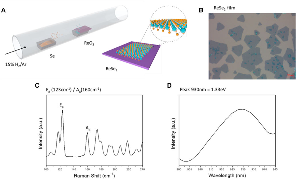
FIGURE 1. Information about synthesized monolayer ReSe2 (A) APCVD schematic for monolayer ReSe2 growth. (B) Optical microscope image of the synthesized ReSe2, the scale bar is 20 µm. (C) Raman spectrum of the monolayer ReSe2. (D) Photoluminescence spectrum of the monolayer ReSe2.
Using a dry oxidation method, SiO2 (300 nm thickness) was deposited on a p-type Si wafer substrate. Half of the substrate was selectively opened by photolithography and etched with a B.O.E 6:1 solution (J.T. Baker). The electrode pattern was defined by photolithography after synthesizing ReSe2. Ti/Au (5 nm/150 nm) metal was deposited onto the device using cluster sputtering (ULVAC SME-200J). Electrical and optoelectronic measurements were conducted using an HP4156A semiconductor parameter analyzer. Laser diodes with varying wavelengths (405, 532, 650, 808, and 1,060 nm) and LEDs with wavelengths ranging from 400 to 1,550 nm were utilized as light sources to assess the device’s spectral response. The light response was analyzed over time using a Thorlabs mechanical chopper (MC 2000B).
The evaluation of photo response to different light intensities is a primary experiment to determine the photodetection performance of the device. Figure 2A shows a schematic of our heterojunction device and 2b shows current versus voltage (I–V) characteristics of the ReSe2/Si photodetector in the dark at different temperatures. The dark current decreases with decreasing temperature due to a decrease in the generation of thermal electrons. The barrier height (0.39 eV) of the ReSe2/Si heterojunction is estimated from the thermionic emission theory of charge carriers. A Richardson plot is drawn using the equation:
where A* is the effective Richardson constant, A is the junction area (0.00005 cm2) of the device, k is Boltzmann’s constant, ϕB is the barrier height of the heterojunction, and T is the temperature, as shown in the inset of Figure 2C. This calculation was carried out in the temperature range of 295–473 K. Figure 2C shows the current versus voltage (I-V) curves of the ReSe2/Si heterojunction for dark and photocurrent at various wavelengths. To verify the enhanced photo-current from ReSe2/Si heterojunction, we conducted separate experiments to compare the photoresponses between the ReSe2/Si heterojunction and Si. Supplementary Figure S3 shows the current changes and ON/OFF ratio for each case and it clearly shows. The high photocurrent was generated in the ReSe2/Si heterojunction, indicating very low photocurrent generated in the Si substrate.
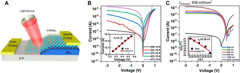
FIGURE 2. (A) A schematic of a ReSe2/Si heterojunction photodetector. (B) I-V characteristics of the ReSe2/Si heterojunction photodiode at various temperatures in the dark. Inset: Ideality factor (n) of 4.8, linear fitting of the I-V curve at the linear regime (represented by dotted line). (C) Dark and photoinduced I-V curves when the photodetector is illuminated with visible (405, 532, 650 nm) and near-infrared (808, 1,060 nm) wavelengths.
Under reverse bias, the photocurrent increases according to the various wavelengths of incident lasers and the corresponding ON/OFF ratios increase significantly, respectively as shown in Figure 3A. As a result of better diode characteristics, under 1,060 nm light illumination (636.6 mW/cm2), the ON/OFF ratio is 5.8 × 10⁴ at open circuit voltage as shown in the inset of Figure 3B. The forward-bias characteristics of the n-p heterojunction diode under dark and light illumination were fitted with the standard diode equation:
where I0, V, q, n, k, and T indicate reverse bias saturation current, voltage, electron charge, ideality factor, Boltzmann constant, and absolute temperature of the heterojunction, respectively. The ideality factor, n provides (inset: Figure 2B) a high value of 4.8 under the dark conditions in the voltage range of 0.25–0.55 V, which is shown with a dotted line in Figure 2B. The high ideality factor indicates the existence of high-density interface defects and trap states in the ReSe2/Si heterojunction. These defects and trap states play an important role in the conduction of photo-generated charge carriers in the device. The photo response of the device is affected by defect trap states at lower illumination intensities.
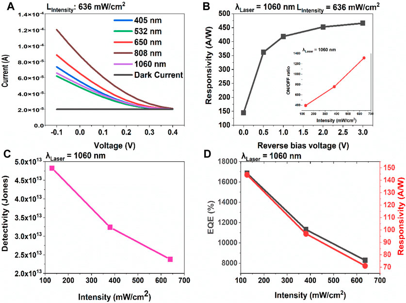
FIGURE 3. The photovoltaic characteristics of the ReSe2 device. (A) Photovoltaic behavior of ReSe2/Si heterojunction. (B) Responsivity of the device under a reverse bias voltage. Inset: Iph/Idark (ON/OFF) ratio at open circuit voltage. (C) Specific detectivity of the device under zero-bias voltage. (D) External quantum efficiency (EQE) and Responsivity as a function of intensity at the open circuit voltage (Voc).
The photovoltaic characteristics of the ReSe2/Si heterojunction were investigated in the intensity range from 127.3 to 636.6 mW/cm2 of 1,060 nm laser illumination, as shown in Figures 3A–D. It is worth noting that the heterojunction exhibits photovoltaic properties under laser illumination without external bias. The significant photovoltaic effect was observed at zero voltage as shown in Figure 3A. The zero-voltage photocurrent highly increased from 1.8 × 10⁻⁵ A at 405 nm to 8.1 × 10⁻⁵ A at 808 nm, indicating that the ReSe2/Si heterojunction device can function as a self-powered photodetector. We investigated the photoresponsivity of this detector as a function of applied reverse bias voltages (V = 0, −0.5, −1, −2, −3 V), as shown in Figure 3B. Under the same incident intensity of 1,060 nm laser illumination, the ReSe2/Si heterojunction exhibited a larger photocurrent at the higher reverse bias. Since the effective barrier height at the ReSe2-Si junction increases with the application of a larger reverse bias, charge separation of the heterojunction is increased by heightened in-built potential. The inset: shows the ON/OFF ratio (5.8 × 10⁴) at Voc. Interestingly, the highest detectivity of the device (4.8 × 10¹³ Jones) is at zero bias due to the lowest dark current when compared to reverse bias voltages, as shown in Figure 3C.
The external quantum efficiency (EQE = hcR/eλ) and responsivity (R = Iph/pA) of the device at different intensities under 1,060 nm illumination are shown in Figure 3D. Here, A is the active area (∼0.00005 cm2) of the device, Iph is the photocurrent, p is the optical power, h is Planck’s constant, e is the electron charge, and c is the speed of light. The EQE and responsivity decrease with increasing light intensity due to interfacial defects and volume trap states in the ReSe2/Si heterojunction. The heterojunction device exhibits a photoresponsivity of R = 144 A/W with a corresponding EQE of 16858% at 0 V under the wavelength of 1,060 nm. These findings reveal that the ReSe2/Si device is useful for the development of advanced photovoltaic devices, such as solar cell applications.
The photocurrent of the ReSe2/Si heterojunction device increases with increasing reverse bias voltage, as shown in Figure 4A. This can be explained by the increased electric field of the ReSe2/Si space charge region with reverse bias, which leads to a decrease in photocarrier transit time and a decrease in recombination of photo-generated charge carriers. Additionally, the photocurrent depends on the intensity of light and follows a power law of Iph = APα, where α = 0.5, 0.7, 0.81, 0.83, and 0.84 at V = 0, −0.5, −1, −2, and −3, respectively. Before electron recombination, it passes through many trap states, and at higher α values (0.84 at −3 V) electrons are separated before recombination by the higher electric field. Therefore, trap-assisted electron excitation is lower compared with lower α values (0.5 at 0 V). Similar behavior of the photocurrent with optical power depending on voltage has been reported for other similar structures (Liu et al., 2016; Yan et al., 2017b; Wei et al., 2017; Lv et al., 2018; Wei et al., 2019).
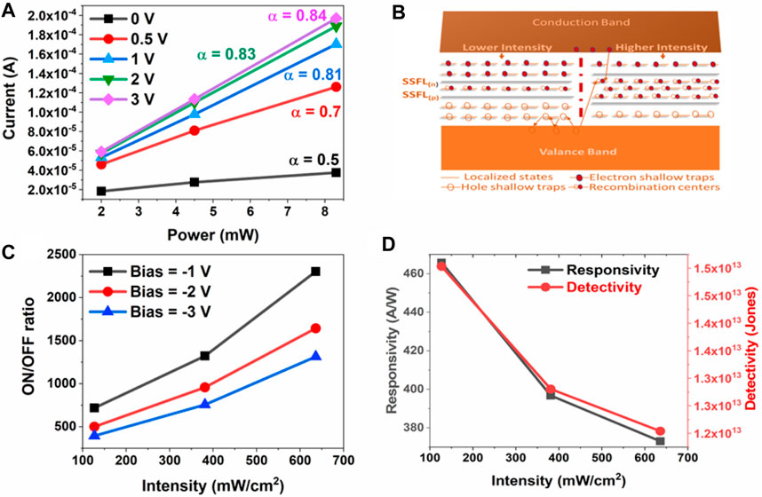
FIGURE 4. (A) Current versus power by bias. (B) Steady-state Fermi level variation with intensity. (C) Voltage-specific ON/OFF ratio based on intensity. (D) Responsivity and specific detectivity of the ReSe2/Si device versus intensity.
The responsivity and detectivity values under different illumination intensities were evaluated and plotted in Figure 4D. The maximum values of responsivity and detectivity were 465 A/W and 1.5 × 10¹³ Jones, respectively, under 1,060 nm at −3 V. The responsivity and detectivity both decreased with increasing light intensity, indicating the presence of localized trap states in the forbidden gap of ReSe2 (Zhu et al., 2021) and Si (Haynes and Hornbeck, 1953). To understand the spreading of the trap states in the forbidden gap of the ReSe2/Si photodetector, optical power dependent Iph was measured at different voltages as shown in Figure 4A. The dependence of Iph on the laser power P (127.3 mW < p < 636.6 mW) followed the power law Iph ∼ Pα with 0.5 < α < 0.84 at different voltages. Lower α values indicate the presence of localized trap states between the conduction and valence bands, as shown in Figure 4B (Rose, 1955; Rose, 1963). These trap states, which exist above the steady state Fermi level for electrons (SSFL)n and below the steady state Fermi level for holes (SSFL)h are called shallow traps. The falling electrons into shallow traps are promptly re-excited into the conduction band by thermal excitations without participating in the recombination process. However, the states that exist between the SSFLn and SSFLh are called deep traps, which are responsible for the recombination of electrons or holes. At higher intensities, the number of photo-excited charge carriers increases, and the two SSFLn and SSFLh move away from each other as shown in Figure 4B, resulting in an increase in the number of recombination centers (Kao, 2004). The increase in the number of recombination centers reduces the lifetime of the free carriers, thereby decreasing the responsivity and detectivity with increasing intensity. At lower intensities, the photocarriers dominate the number of recombination centers, leading to higher responsivity through the re-excitation of trapped electrons into the conduction band (Shi et al., 2013). Figure 4C shows the positive dependence of the ON/OFF ratio on the illumination intensity for different voltages. The maximum ON/OFF ratio of the heterojunction was about 2303 at −1 V reverse bias. The ON/OFF ratio decreased with increasing negative bias voltage at constant optical power density because the dark current decreased with an increase in negative voltage, while photocurrent increased due to the wide depletion region. It also showed a higher on-off ratio, up to 57920 at 0 V bias (shown in Supplementary Figure S5).
The spectral responsivity of the ReSe2/Si heterojunction is shown in Figure 5A. Remarkably, the heterojunction exhibits a broad spectral response that covers the entire visible and infrared wavelength range due to its unique band alignment, which facilitates the direct transition of valence electrons of Si to the conduction band of ReSe2. The peak responsivity of the heterojunction is observed to be 465 A/W at 1,060 nm, as shown in Figure 5A. The detectivity exhibits a similar trend to the responsivity with a maximum value of 1.5 × 10¹³ Jones at −3 V as shown in Figure 5A. The spectral behavior of EQE is also presented in Figure 5B, where the maximum EQE value of 54368% is achieved at 1,060 nm. The broadband response from 400 nm to 1,100 nm wavelength under LED light source is shown in Supplementary Figure S4 and the highest responsivity of 1056 A/W was measured at 1,000 nm.
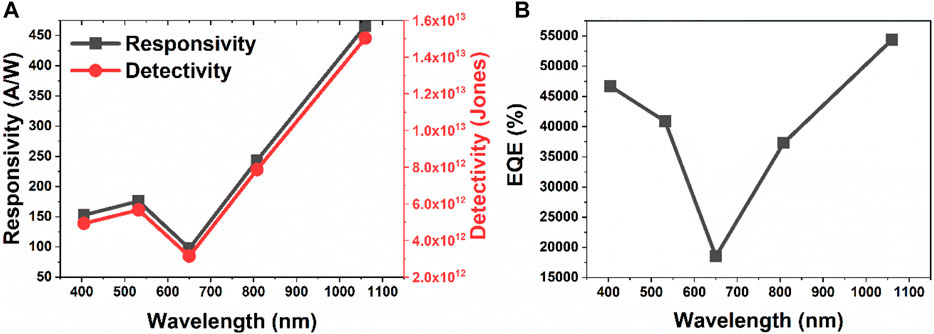
FIGURE 5. (A) Responsivity and specific detectivity of the ReSe2/Si device versus wavelength. (B) Wavelength-dependent external quantum efficiency under 1,060 nm laser light at −3 V reverse bias.
The band alignment of Si and ReSe2 before contact is shown in Figure 6A. The electron affinities of ReSe2 and Si are 3.9 and 4.05 eV, respectively. ReSe2 exhibits an n-type behavior with a layer-independent indirect band gap (1.31 eV) (Jariwala et al., 2016b; Hart et al., 2017) and Si also has an indirect band gap of 1.12 eV. The Fermi level (Ef) of ReSe2 is located close to the conduction band (Ec), while the Fermi level of p-type Si is close to the valence band (Ev). Upon contact, a p-n heterojunction is formed, and the diffusion of electrons and holes leads to the local band bending at the interface between ReSe2 and Si. Furthermore, the equilibrium of carrier diffusion at the heterojunction interface causes the Ef of both semiconductors to reach the same level. The band alignment of the heterojunction after contact is presented in Figure 6B, where electrons transfer from ReSe2 to Si, and holes in Si transfer in the opposite direction due to the difference between Fermi levels (ϕB = 0.39 eV). Figure 6C shows the band offset of the heterojunction under reverse bias with light illumination. Photoexcited electrons are generated in ReSe2 and Si under 405–1,060 nm laser light illumination. Under the external reverse bias, the direction of the electric field of the barrier potential in the ReSe2/Si heterojunction aligns with the applied electric field. Additionally, the staggered gaps (Type II) band offset causes photoelectrons in Si to flow into ReSe2, while the holes flow in the opposite direction. Finally, under laser illumination, the photo-generated carriers are collected by the electrodes.

FIGURE 6. Energy band diagrams of the ReSe2/Si heterojunction (A) Before contact (B) After contact (C) After illumination under reverse bias operation.
We have fabricated a heterojunction photodiode by depositing a ReSe2 monolayer on p-type silicon and applying Ti/Au contacts. We have investigated the photovoltaic and photo response properties of the device illumination with different wavelengths and intensities. Our results show that interface and subgap states strongly affect the device’s photocurrent, with these traps re-exciting trapped electrons into the conduction band at lower intensities. The ReSe2/Si heterojunction exhibits excellent spectral selectivity, long-term stability, and good reproducibility. We have measured an ON/OFF ratio of 5.8 × 10⁴, a responsivity of 465 A/W, and a detectivity of 4.8 × 10¹³, indicating the photovoltaic behavior of the device. The device exhibits a low dark current of 1.4 × 10⁻⁹ A and a high external quantum efficiency of 54368.2% at −3 V under 1,060 nm laser light, representing a photoconductive gain. The maximum photoresponsivity (R = 465 A/W) is achieved at reverse bias of −3 V under 1,060 nm illumination.
The original contributions presented in the study are included in the article/Supplementary Material, further inquiries can be directed to the corresponding authors.
BJ: Data curation, Visualization, Writing–original draft, Writing–review and editing. KS: Methodology, Visualization, Writing–original draft. KP: Investigation, Methodology, Writing–original draft. CJ: Data curation, Writing–original draft. BP: Formal Analysis, Writing–review and editing. ML: Writing–review and editing. SR: Supervision, Writing–original draft, Writing–review and editing. MH: Funding acquisition, Supervision, Writing–review and editing. YK: Supervision, Writing–review and editing, Funding acquisition.
The author(s) declare that no financial support was received for the research, authorship, and/or publication of this article.
YK acknowledges the financial support from the Semiconductor R&D Support Project through the Gangwon Technopark (GWTP) funded by Gangwon Province (No. GWTP 2023-027). MH acknowledges the financial support from Inha University Research Grant 2022 (67853-1).
The authors declare that the research was conducted in the absence of any commercial or financial relationships that could be construed as a potential conflict of interest.
The author(s) declared that they were an editorial board member of Frontiers, at the time of submission. This had no impact on the peer review process and the final decision.
All claims expressed in this article are solely those of the authors and do not necessarily represent those of their affiliated organizations, or those of the publisher, the editors and the reviewers. Any product that may be evaluated in this article, or claim that may be made by its manufacturer, is not guaranteed or endorsed by the publisher.
The Supplementary Material for this article can be found online at: https://www.frontiersin.org/articles/10.3389/fmats.2024.1354522/full#supplementary-material
Arora, A., Noky, J., DruPpel, M., Jariwala, B., Deilmann, T., Schneider, R., et al. (2017). Highly anisotropic in-plane excitons in atomically thin and bulklike 1 T′-ReSe2. Nano Lett. 17, 3202–3207. doi:10.1021/acs.nanolett.7b00765
Chenais, N. a.L., Airaghi Leccardi, M. J. I., and Ghezzi, D. (2021). Photovoltaic retinal prosthesis restores high-resolution responses to single-pixel stimulation in blind retinas. Commun. Mater. 2, 28. doi:10.1038/s43246-021-00133-2
Dong, R., Bi, C., Dong, Q., Guo, F., Yuan, Y., Fang, Y., et al. (2014). An ultraviolet-to-NIR broad spectral nanocomposite photodetector with gain. Adv. Opt. Mater. 2, 549–554. doi:10.1002/adom.201400023
García-Hemme, E., García-Hernansanz, R., Olea, J., Pastor, D., Del Prado, A., Mártil, I., et al. (2014). Room-temperature operation of a titanium supersaturated silicon-based infrared photodetector. Appl. Phys. Lett. 104, 211105. doi:10.1063/1.4879851
Gupta, S., and Kumar, R. (2022). Review—photodetection properties of graphene/silicon van der Waals heterojunction. ECS J. Solid State Sci. Technol. 11, 061010. doi:10.1149/2162-8777/ac7614
Hart, L., Dale, S., Hoye, S., Webb, J. L., and Wolverson, D. (2016). Rhenium dichalcogenides: layered semiconductors with two vertical orientations. Nano Lett. 16, 1381–1386. doi:10.1021/acs.nanolett.5b04838
Hart, L. S., Webb, J. L., Dale, S., Bending, S. J., Mucha-Kruczynski, M., Wolverson, D., et al. (2017). Electronic bandstructure and van der Waals coupling of ReSe2 revealed by high-resolution angle-resolved photoemission spectroscopy. Sci. Rep. 7, 5145. doi:10.1038/s41598-017-05361-6
Hasani, A., Le, Q. V., Tekalgne, M., Choi, M.-J., Lee, T. H., Jang, H. W., et al. (2019). Direct synthesis of two-dimensional MoS2 on p-type Si and application to solar hydrogen production. NPG Asia Mater. 11, 47. doi:10.1038/s41427-019-0145-7
Haynes, J., and Hornbeck, J. (1953). Temporary traps in silicon and germanium. Phys. Rev. 90, 152–153. doi:10.1103/physrev.90.152.2
Jariwala, B., Thamizhavel, A., and Bhattacharya, A. (2016a). ReSe2: a reassessment of crystal structure and thermal analysis. J. Phys. D Appl. Phys. 50, 044001. doi:10.1088/1361-6463/aa5062
Jariwala, B., Voiry, D., Jindal, A., Chalke, B. A., Bapat, R., Thamizhavel, A., et al. (2016b). Synthesis and characterization of ReS2 and ReSe2 layered chalcogenide single crystals. Chem. Mater. 28, 3352–3359. doi:10.1021/acs.chemmater.6b00364
Jiang, S., Zhang, Z., Zhang, N., Huan, Y., Gong, Y., Sun, M., et al. (2018). Application of chemical vapor–deposited monolayer ReSe 2 in the electrocatalytic hydrogen evolution reaction. Nano Res. 11, 1787–1797. doi:10.1007/s12274-017-1796-8
Li, X., Chen, C., Yang, Y., Lei, Z., and Xu, H. (2020). 2D Re-based transition metal chalcogenides: progress, challenges, and opportunities. Adv. Sci. 7, 2002320. doi:10.1002/advs.202002320
Liu, E., Fu, Y., Wang, Y., Feng, Y., Liu, H., Wan, X., et al. (2015). Integrated digital inverters based on two-dimensional anisotropic ReS2 field-effect transistors. Nat. Commun. 6, 6991. doi:10.1038/ncomms7991
Liu, F., Zheng, S., He, X., Chaturvedi, A., He, J., Chow, W. L., et al. (2016). Highly sensitive detection of polarized light using anisotropic 2D ReS2. Adv. Funct. Mater. 26, 1169–1177. doi:10.1002/adfm.201504546
Lv, Q., Yan, F., Wei, X., and Wang, K. (2018). High-performance, self-driven photodetector based on graphene sandwiched GaSe/WS2 heterojunction. Adv. Opt. Mater. 6, 1700490. doi:10.1002/adom.201700490
Pradhan, N. R., Garcia, C., Isenberg, B., Rhodes, D., Feng, S., Memaran, S., et al. (2018). Phase modulators based on high mobility ambipolar ReSe2 field-effect transistors. Sci. Rep. 8, 12745. doi:10.1038/s41598-018-30969-7
Rogalski, A. (2002). Infrared detectors: an overview. Infrared Phys. Technol. 43, 187–210. doi:10.1016/s1350-4495(02)00140-8
Rose, A. (1955). Recombination processes in insulators and semiconductors. Phys. Rev. 97, 322–333. doi:10.1103/physrev.97.322
Rose, A. (1963). Concepts in photoconductivity and allied problems. Switzerland: Interscience publishers.
Shelke, N. T., Karle, S., and Karche, B. (2020). Photoresponse properties of CdSe thin film photodetector. J. Mater. Sci. Mater. Electron. 31, 15061–15069. doi:10.1007/s10854-020-04069-0
Shi, H., Yan, R., Bertolazzi, S., Brivio, J., Gao, B., Kis, A., et al. (2013). Exciton dynamics in suspended monolayer and few-layer MoS2 2D crystals. ACS Nano 7, 1072–1080. doi:10.1021/nn303973r
Sun, H., Lei, T., Tian, W., Cao, F., Xiong, J., and Li, L. (2017). Self-powered, flexible, and solution-processable perovskite photodetector based on low-cost carbon cloth. Small 13, 1701042. doi:10.1002/smll.201701042
Sun, M., Fang, Q., Xie, D., Sun, Y., Qian, L., Xu, J., et al. (2018). Heterostructured graphene quantum dot/WSe 2/Si photodetector with suppressed dark current and improved detectivity. Nano Res. 11, 3233–3243. doi:10.1007/s12274-017-1855-1
Wei, X., Yan, F., Lv, Q., Shen, C., and Wang, K. (2017). Fast gate-tunable photodetection in the graphene sandwiched WSe 2/GaSe heterojunctions. Nanoscale 9, 8388–8392. doi:10.1039/c7nr03124f
Wei, X., Yan, F., Lv, Q., Zhu, W., Hu, C., Patanè, A., et al. (2019). Enhanced photoresponse in MoTe2 photodetectors with asymmetric graphene contacts. Adv. Opt. Mater. 7, 1900190. doi:10.1002/adom.201900190
Yan, C., Gan, L., Zhou, X., Guo, J., Huang, W., Huang, J., et al. (2017a). Space-confined chemical vapor deposition synthesis of ultrathin HfS2 flakes for optoelectronic application. Adv. Funct. Mater. 27, 1702918. doi:10.1002/adfm.201702918
Yan, F., Zhao, L., Patanè, A., Hu, P., Wei, X., Luo, W., et al. (2017b). Fast, multicolor photodetection with graphene-contacted p-GaSe/n-InSe van der Waals heterostructures. Nanotechnology 28, 27LT01. doi:10.1088/1361-6528/aa749e
Yu, T., Wang, F., Xu, Y., Ma, L., Pi, X., and Yang, D. (2016). Graphene coupled with silicon quantum dots for high-performance bulk-silicon-based Schottky-junction photodetectors. Adv. Mater. 28, 4912–4919. doi:10.1002/adma.201506140
Keywords: ReSe2, photodetector, heterojunction, high photoconductive gain, broadband photodetector
Citation: Jo B, Seo K, Park K, Jeong C, Poornaprakash B, Lee M, Ramu S, Hahm MG and Kim YL (2024) Trap-assisted monolayer ReSe2/Si heterojunction with high photoconductive gain and self-driven broadband photodetector.. Front. Mater. 11:1354522. doi: 10.3389/fmats.2024.1354522
Received: 12 December 2023; Accepted: 29 January 2024;
Published: 15 February 2024.
Edited by:
Hock Jin Quah, University of Science Malaysia, MalaysiaReviewed by:
Lakshmi Narayanan Mosur Saravana Murthy, Intel, United StatesCopyright © 2024 Jo, Seo, Park, Jeong, Poornaprakash, Lee, Ramu, Hahm and Kim. This is an open-access article distributed under the terms of the Creative Commons Attribution License (CC BY). The use, distribution or reproduction in other forums is permitted, provided the original author(s) and the copyright owner(s) are credited and that the original publication in this journal is cited, in accordance with accepted academic practice. No use, distribution or reproduction is permitted which does not comply with these terms.
*Correspondence: Singiri Ramu, c2ltZ2lyaS5yYW11QGdtYWlsLmNvbQ==; Myung Gwan Hahm, bWdoYWhtQGluaGEuYWMua3I=; Young Lae Kim, eWxraW1AZ3dudS5hYy5rcg==
†These authors have contributed equally to this work and share first authorship
Disclaimer: All claims expressed in this article are solely those of the authors and do not necessarily represent those of their affiliated organizations, or those of the publisher, the editors and the reviewers. Any product that may be evaluated in this article or claim that may be made by its manufacturer is not guaranteed or endorsed by the publisher.
Research integrity at Frontiers
Learn more about the work of our research integrity team to safeguard the quality of each article we publish.