 Zheng Liu
 Yuxin Liu2
 Hongxuan Guo
94% of researchers rate our articles as excellent or good
Learn more about the work of our research integrity team to safeguard the quality of each article we publish.
Find out more
ORIGINAL RESEARCH article
Front. Mater., 28 September 2023
Sec. Polymeric and Composite Materials
Volume 10 - 2023 | https://doi.org/10.3389/fmats.2023.1279939
This article is part of the Research TopicOrdered Structures of Nanomaterials in Advanced CompositesView all 4 articles
The cleanliness of transferred graphene is crucial for its application in various fields. The presence of residues of polymethyl methacrylate (PMMA) on the surface of transferred graphene has a negative impact on its transparency, transport, and other critical properties. In this study, we propose an alternative method to reduce such residues by using acetic acid instead of the commonly used acetone. The effects of treating graphene with acetic acid and acetone are comprehensively evaluated through optical microscopy, scanning electron microscopy, Raman spectroscopy, and X-ray photoelectron spectroscopy. The results of this study demonstrate a significant reduction in surface residue when graphene is treated with acetic acid, compared to acetone treatment. Additionally, we applied this method to fabricate graphene-based supercapacitors and compared the results using acetic acid and acetone. This reduction in residue holds great promise for advancing the development of high-quality graphene devices.
Graphene is an emerging material with a single-atom thickness and a two-dimensional honeycomb lattice structure. Due to its excellent optical, mechanical, and electrical properties, graphene has attracted the interest of researchers in materials science. It has applications and potential in various fields, including field effect transistors (Britnell et al., 2012; Vicarelli et al., 2012; Liu et al., 2018; Jiang et al., 2019), sensors (He et al., 2012; Liu et al., 2012; Wu et al., 2013; Yang et al., 2018), photovoltaic devices (Freitag et al., 2013; Liu et al., 2015; Wang and Shi, 2015), and optoelectronics (Gu et al., 2012; Ye et al., 2013; Tan et al., 2020). CVD graphene grown on copper or nickel substrates is widely used due to its large area and good uniformity (Li et al., 2009; Li et al., 2011; Zhang et al., 2013). Various methods have been developed for transferring CVD graphene from metal foils to different substrates (Lin et al., 2011; Suk et al., 2011; Yulaev et al., 2016; Schranghamer et al., 2021). The transfer is usually accomplished using a polymer support layer to prevent the folding or tearing of graphene during the transfer process. The preferred method for transferring graphene is the polymer-assisted wet transfer method, which uses PMMA as a support, due to its experimental convenience and high transfer yield.
However, in this transfer method, the removal of PMMA is a critical and challenging step to achieve clean graphene transfer. This is primarily because of the presence of PMMA residues. The electrical properties of graphene, which is a single atom-thin and two-dimensional material, are directly affected by the electronic interactions with neighboring molecules. Unfortunately, acetone is not able to completely remove PMMA and often leaves behind residues on the graphene or substrate (Lin et al., 2012). These residues can disrupt the uniformity and alter the electrical properties of graphene (Deng et al., 2014), impacting its applications in electronic devices and sensors. Various methods have been proposed to eliminate PMMA residues, including thermal annealing in gas or vacuum (Ahn et al., 2013; Tripathi et al., 2017), electron beam treatment (Son et al., 2017), and ion beam treatment (Kim et al., 2016). However, these methods are complex to implement or can only clean specific areas, and some may even damage the graphene.
In this paper, we present a methodology that employs acetic acid as an organic solvent for cleaning PMMA, and we compare its effectiveness with the use of acetone. Next, we conduct a characterization of the samples utilizing multiple techniques including optical microscopy, Raman spectroscopy, scanning electron microscopy, and X-ray photoelectron spectroscopy. Furthermore, we apply this methodology to fabricate supercapacitors based on graphene and analyze their performance.
The PMMA-coated copper-based graphene films were obtained from Nanjing XFNANO Materials Company. Following the standard wet transfer method for graphene (Suk et al., 2011), a 20 μm copper foil with a monolayer graphene coating was immersed in a 0.2 mol/L solution of ammonium persulfate at 50°C for 1 h, resulting in the complete dissolution of the copper foil. The PMMA/graphene stack was then rinsed multiple times with deionized water to remove any residual copper ions beneath the graphene layer, and subsequently transferred onto a silicon oxide wafer for further processing. The transferred samples were air-dried for 1 h to remove any moisture on the substrate and then heated at 200°C for 1 h to enhance adhesion between the graphene and the silicon oxide substrate. Afterward, the samples underwent separate washing steps using acetone and acetic acid. The samples treated with acetone were washed in acetone at 50°C for 3 h, while the samples treated with acetic acid were washed in acetic acid at room temperature for 3 h. Finally, the samples were cleaned using an isopropyl alcohol solution.
To fabricate graphene-based supercapacitors, 1 g of polymethyl methacrylate (PMMA) (Aladdin, Mw ∼ general injection grade) was mixed with 25 mL of acetone to synthesize a gel electrolyte solution. The mixture was heated to 60°C and continuously stirred until it became transparent. Then, 4 g of 1-ethyl-3-methylimidazolium bis(trifluoromethylsulfonyl)imide ([EMIM][TFSI]) (Beijing Cool Chemical Technology Co., Ltd.) were added to the mixture and stirred for another 30 min. Finally, the mixture was allowed to cool to room temperature, resulting in a gel electrolyte solution.
Copper-based graphene samples containing PMMA were washed in acetone at 50°C for 3 h, while another set of copper-based graphene samples was washed in acetic acid at room temperature for 3 h. Both sets of samples were then rinsed with an isopropanol solution and dried. The gel electrolyte solution was then spin-coated and heated at 60°C for 3 h, after which Gallium-indium-tin liquid metal (Dongguan Qiaotai Metal Technology Co., Ltd.) was added as the electrode.
Scanning electron microscopy (SEM) was employed to examine the PMMA residues, aiming to evaluate the distinctions resulting from the application of either acetone or acetic acid for cleaning graphene. Additionally, Raman spectroscopy and X-ray photoelectron spectroscopy were employed to analyze the PMMA residues on the graphene surface. The electrochemical characteristics of supercapacitors utilizing both cleaning methods were evaluated by analyzing the cyclic voltammetry (CV) curves.
The optical images in Figures 1A,B were captured using a light microscope after cleaning with acetone and acetic acid, respectively. It is evident from the figures that both cleaning methods did not cause noticeable damage to the graphene, but residual PMMA polymer residues were clearly visible. Figures 1C,D shows selected areas magnified 20,000 times using SEM, revealing the size and quantity of PMMA residues. Each SEM image was estimated to have an area of approximately 4.25 × 6.35 μm using a ruler. The density of PMMA residue and impurities on the graphene surface was then calculated after cleaning with acetone and acetic acid. As measuring with the optical images, the area percentage of PMMA residue on graphene after acetone cleaning is 0.592% and after acetic acid cleaning is 0.157%. It is evident that the residual density of PMMA on the graphene surface, treated with acetic acid, is lower compared to that after acetone treatment. This highlights the superior effectiveness of acetic acid in cleaning PMMA residues on the graphene surface.
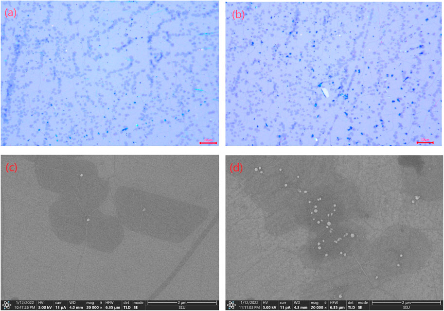
FIGURE 1. Image of graphene sample transferred to a silicon oxide substrate. (A), (B): Optical microscopy images by acetic acid and acetone treatment. (C), (D): SEM images by acetic acid and acetone treatment.
Raman spectroscopy plays a crucial role in the investigation of graphene, particularly in the study of graphene transfer. It provides information about the quality of graphene and the structural changes that occur during transfer. This information facilitates the evaluation and optimization of transfer techniques to achieve high-quality graphene films. Figure 2 presents the Raman spectra obtained from graphene samples treated with acetone and acetic acid, using a 532 nm laser as the light source. The presence of a D peak around 1,350 cm−1 in the Raman spectrum indicates disordered vibrations in graphene (Wu et al., 2018), which are typically associated with graphene defects. One notable observation is that the graphene samples subjected to treatments with acetic acid and acetone exhibit smaller differences in the intensity of the D peak. This implies that our method does not yield significant enhancements in the quality of transferred graphene, rather emphasizing the cleanliness of the transferred graphene. Furthermore, the Raman spectrum shows a G peak at 1,580 cm−1 and a 2D peak at 2,700 cm−1 (Ferrari and Basko, 2013). Importantly, the intensity ratio of I2D/IG remains approximately 2 in both cases. This suggests that there is no significant variation and confirms the characteristic features of single-layer graphene.
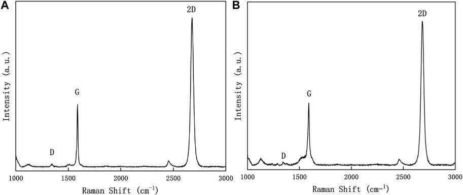
FIGURE 2. Raman spectra of graphene sample transferred to silicon oxide substrate. (A): acetic acid treatment, (B): acetone treatment.
The C 1s core level spectra of transferred monolayer and bilayer graphene samples were presented in Figure 3. To subtract the background, the Shirley algorithm was used before fitting the spectrum with a Gaussian Lorentzian peak. The spectrum shows chemical bonds arising from sp2 and sp3 hybridization of carbon bonds in graphene, as well as various functional groups in PMMA residues. The C 1s spectrum comprises five components: a peak around 284.3 ± 0.1 eV representative of sp2 hybridization of C-C bonds in graphene, a peak around 285 ± 0.1 eV representing sp3 hybridization of defects in graphene and C-C bonds in PMMA residues (Pirlot et al., 2002). Additionally, there are peaks around 285.6 ± 0.1 eV, 286.7 ± 0.1 eV, and 288.9 ± 0.1 eV corresponding to C-C bonds, C-O bonds, and O-C=O bonds in the PMMA residue (Dí et al., 1996; Du et al., 2002; Deng et al., 2014; Gross et al., 1993). The binding energy and peak area ratio of the various C 1s components are displayed in Table 1. Both the figure and table indicate that the PMMA residue remained on the graphene even after the cleaning process. Furthermore, it can be observed from Figure 3 and Tables 1 and 2 that the acetic acid-cleaned graphene samples, whether single-layer or double-layer, display higher peak area ratios of carbon sp2 hybridization associated with graphene. In contrast, the peak area ratios of C-C bonds, C-O bonds, and O-C=O bonds characteristic of residual groups in PMMA are smaller, which conclusively demonstrates that the acetic acid-cleaned samples have less PMMA residue compared to the acetone-cleaned samples.
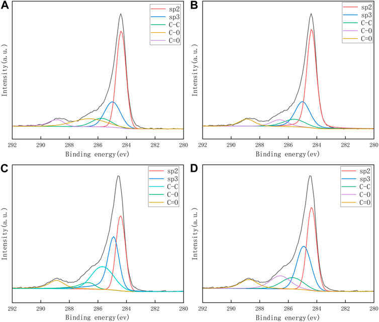
FIGURE 3. XPS spectra of graphene sample transferred to silicon oxide substrate. (A, B): Single-layer graphene (SLG) and bilayer graphene (BLG) of acetic acid treatment, (C, D): SLG and BLG of acetone treatment.
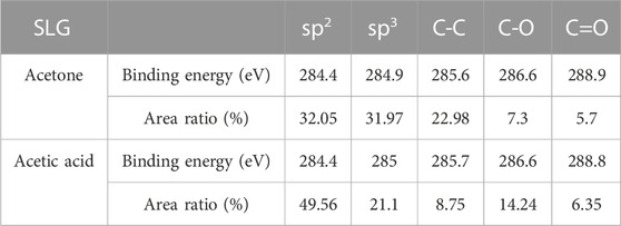
TABLE 1. Binding energy and peak area ratio of the various components of C 1s in the monolayer graphene samples.
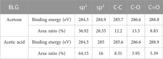
TABLE 2. Binding energy and peak area ratios of the various components of C 1s in the bilayer graphene samples.
The testing of supercapacitors plays a crucial role in evaluating their performance and potential applications in various fields. In the study, the procedure for fabricating graphene-based supercapacitors in CVD graphene is demonstrated in Figure 4A. Firstly, the copper-based graphene electrode is liberated from PMMA by employing acetone and acetic acid as solvents. Subsequently, a gel-electrolyte film is formed through spin-coating, and then a liquid metal drop is applied as the electrode. To illustrate the internal structure, Figure 4B presents a cross-sectional view of the graphene-based supercapacitor with a conventional sandwich configuration, comprised of copper/gel electrolyte/liquid metal. By following this fabrication method, the researchers were able to obtain graphene-based supercapacitors for further examination and analysis.
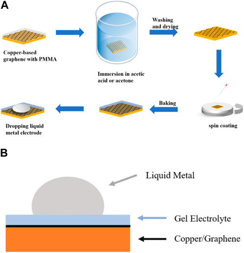
FIGURE 4. (A) Schematic diagram of graphene-based supercapacitor fabrication. (B) Schematic structure of a supercapacitor.
The CV curves of graphene-based supercapacitors using different cleaning methods for PMMA are depicted in Figure 5. The red line corresponds to the utilization of acetic acid, while the black line represents the utilization of acetone. The supercapacitor underwent scanning between ±0.2 V with a scan rate of 0.1 V/s. The graph clearly demonstrates that the acetic acid cleaning method exhibits higher charging and discharging currents. Based on this data, the capacitance of the acetic acid sample is calculated to be 5.01 μF/cm2, whereas the acetone sample demonstrates a capacitance of 3.37 μF/cm2. This discrepancy in capacitance values can be attributed to variations in the cleanliness levels of the graphene samples, specifically the residue affecting the electrode resistance and the double layer capacitance at the interface.
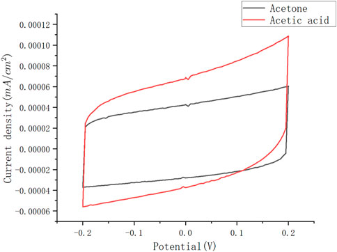
FIGURE 5. CV curves of supercapacitors treated with acetic acid and acetone, respectively.
In conclusion, we conducted a systematic investigation into the impact of transfer conditions on the PMMA-assisted graphene transfer method. The graphene samples treated with acetic acid exhibited a lower presence of PMMA residue compared to those treated with acetone, effectively reducing the amount of PMMA. This was confirmed through scanning electron microscopy and x-ray photoelectron spectroscopy analyses. Furthermore, we applied this method in the fabrication of graphene-based supercapacitors, demonstrating the significant difference in cleanliness achieved. The simplicity of this method offers clean graphene samples with minimal PMMA residues, thereby enhancing the electrical properties and surface uniformity of graphene. Moreover, it facilitates the practical implementation of graphene in various device applications.
The original contributions presented in the study are included in the article/supplementary material, further inquiries can be directed to the corresponding authors.
ZL: Conceptualization, Data curation, Writing–original draft, Writing–review and editing. YL: Writing–review and editing. WZ: Methodology, Writing–review and editing. YD: Investigation, Writing–review and editing. WL: Data curation, Writing–review and editing. YW: Writing–review and editing. HG: Investigation, Writing–review and editing, Conceptualization. JH: Conceptualization, Methodology, Writing–review and editing.
The author(s) declare that no financial support was received for the research, authorship, and/or publication of this article.
The authors acknowledge financial support from the National Natural Science Foundation of China (Grant Nos. 11874105), the Fundamental Research Funds for the Central Universities, the Science and Technology Project of Jiangsu Provincial Administration for Market Regulation (KJ21125057), the Independent Research Project of Large Scientific Instruments of Jiangsu Province (Advances in XPS Characterization Techniques for Graphene and Low-Dimensional Materials).
The authors declare that the research was conducted in the absence of any commercial or financial relationships that could be construed as a potential conflict of interest.
All claims expressed in this article are solely those of the authors and do not necessarily represent those of their affiliated organizations, or those of the publisher, the editors and the reviewers. Any product that may be evaluated in this article, or claim that may be made by its manufacturer, is not guaranteed or endorsed by the publisher.
Ahn, Y., Kim, H., Kim, Y. H., Yi, Y., and Kim, S. I. (2013). Procedure of removing polymer residues and its influences on electronic and structural characteristics of graphene. Appl. Phys. Lett. 102 (9), 091602. doi:10.1063/1.4794900
Britnell, L., Gorbachev, R. V., Jalil, R., Belle, B. D., Schedin, F., Mishchenko, A., et al. (2012). Field-effect tunneling transistor based on vertical graphene heterostructures. Science 335 (6071), 947–950. doi:10.1126/science.1218461
Deng, C., Lin, W., Agnus, G., Dragoe, D., Pierucci, D., Ouerghi, A., et al. (2014). Reversible charge-transfer doping in graphene due to reaction with polymer residues. J. Phys. Chem. C 118 (25), 13890–13897. doi:10.1021/jp501077t
Díaz, J., Paolicelli, G., Ferrer, S., and Comin, F. (1996). Separation of the sp3 and sp2 components in the C1s photoemission spectra of amorphous carbon films. Phys. Rev. B 54 (11), 8064–8069. doi:10.1103/physrevb.54.8064
Du, J., Zhu, J., Wilkie, C. A., and Wang, J. (2002). An XPS investigation of thermal degradation and charring on PMMA clay nanocomposites. Polym. Degrad. Stab. 77 (3), 377–381. doi:10.1016/s0141-3910(02)00074-5
Ferrari, A. C., and Basko, D. M. (2013). Raman spectroscopy as a versatile tool for studying the properties of graphene. Nat. Nanotechnol. 8 (4), 235–246. doi:10.1038/nnano.2013.46
Freitag, M., Low, T., Xia, F., and Avouris, P. (2013). Photoconductivity of biased graphene. Nat. Photonics 7 (1), 53–59. doi:10.1038/nphoton.2012.314
Gross, T., Lippitz, A., Unger, W., Wöll, C., Hähner, G., and Braun, W. (1993). Some remarks on fitting standard-and high resolution C 1s and O 1s x-ray photoelectron spectra of PMMA. Appl. Surf. Sci. 68 (3), 291–298. doi:10.1016/0169-4332(93)90248-a
Gu, T., Petrone, N., McMillan, J. F., van der Zande, A., Yu, M., Lo, G. Q., et al. (2012). Regenerative oscillation and four-wave mixing in graphene optoelectronics. Nat. Photonics 6 (8), 554–559. doi:10.1038/nphoton.2012.147
He, Q., Wu, S., Yin, Z., and Zhang, H. (2012). Graphene-based electronic sensors. Chem. Sci. 3 (6), 1764–1772. doi:10.1039/c2sc20205k
Jiang, S., Li, L., Wang, Z., Shan, J., and Mak, K. F. (2019). Spin tunnel field-effect transistors based on two-dimensional van der Waals heterostructures. Nat. Electron. 2 (4), 159–163. doi:10.1038/s41928-019-0232-3
Kim, K. S., Oh, I. K., Jung, H., Kim, H., and Yeom, G. Y. (2016). Atomic layer deposition of HfO2 on graphene through controlled ion beam treatment. Appl. Phys. Lett. 108 (21), 213102. doi:10.1063/1.4950997
Li, X., Cai, W., An, J., Kim, S., Nah, J., Yang, D., et al. (2009). Large-area synthesis of high-quality and uniform graphene films on copper foils. science 324 (5932), 1312–1314. doi:10.1126/science.1171245
Li, X., Magnuson, C. W., Venugopal, A., Tromp, R. M., Hannon, J. B., Vogel, E. M., et al. (2011). Large-area graphene single crystals grown by low-pressure chemical vapor deposition of methane on copper. J. Am. Chem. Soc. 133 (9), 2816–2819. doi:10.1021/ja109793s
Lin, Y-C., Jin, C., Lee, J. C., Jen, S. F., Suenaga, K., and Chiu, P. W. (2011). Clean transfer of graphene for isolation and suspension. ACS Nano 5 (3), 2362–2368. doi:10.1021/nn200105j
Lin, Y-C., Lu, C. C., Yeh, C. H., Jin, C., Suenaga, K., and Chiu, P. W. (2012). Graphene annealing: how clean can it be? Nano Lett. 12 (1), 414–419. doi:10.1021/nl203733r
Liu, Y., Duan, X., Huang, Y., and Duan, X. (2018). Two-dimensional transistors beyond graphene and TMDCs. Chem. Soc. Rev. 47 (16), 6388–6409. doi:10.1039/c8cs00318a
Liu, Y., Dong, X., and Chen, P. (2012). Biological and chemical sensors based on graphene materials. Chem. Soc. Rev. 41 (6), 2283–2307. doi:10.1039/c1cs15270j
Liu, Z., Lau, S. P., and Yan, F. (2015). Functionalized graphene and other two-dimensional materials for photovoltaic devices: device design and processing. Chem. Soc. Rev. 44 (15), 5638–5679. doi:10.1039/c4cs00455h
Pirlot, C., Willems, I., Fonseca, A., Nagy, J., and Delhalle, J. (2002). Preparation and characterization of carbon nanotube/polyacrylonitrile composites. Adv. Eng. Mater. 4 (3), 109–114. doi:10.1002/1527-2648(200203)4:3<109::aid-adem109>3.0.co;2-5
Schranghamer, T. F., Sharma, M., Singh, R., and Das, S. (2021). Review and comparison of layer transfer methods for two-dimensional materials for emerging applications. Chem. Soc. Rev. 50, 11032–11054. doi:10.1039/d1cs00706h
Son, B. H., Kim, H. S., Jeong, H., Park, J. Y., Lee, S., and Ahn, Y. H. (2017). Electron beam induced removal of PMMA layer used for graphene transfer. Sci. Rep. 7 (1), 18058–18067. doi:10.1038/s41598-017-18444-1
Suk, J. W., Kitt, A., Magnuson, C. W., Hao, Y., Ahmed, S., An, J., et al. (2011). Transfer of CVD-grown monolayer graphene onto arbitrary substrates. ACS Nano 5 (9), 6916–6924. doi:10.1021/nn201207c
Tan, T., Jiang, X., Wang, C., Yao, B., and Zhang, H. (2020). 2D material optoelectronics for information functional device applications: status and challenges. Adv. Sci. 7 (11), 2000058. doi:10.1002/advs.202000058
Tripathi, M., Mittelberger, A., Mustonen, K., Mangler, C., Kotakoski, J., Meyer, J. C., et al. (2017). Cleaning graphene: comparing heat treatments in air and in vacuum. Phys. status solidi (RRL)–Rapid Res. Lett. 11 (8), 1700124. doi:10.1002/pssr.201700124
Vicarelli, L., Vitiello, M. S., Coquillat, D., Lombardo, A., Ferrari, A. C., Knap, W., et al. (2012). Graphene field-effect transistors as room-temperature terahertz detectors. Nat. Mater. 11 (10), 865–871. doi:10.1038/nmat3417
Wang, X., and Shi, G. (2015). Flexible graphene devices related to energy conversion and storage. Energy and Environ. Sci. 8 (3), 790–823. doi:10.1039/c4ee03685a
Wu, J-B., Lin, M. L., Cong, X., Liu, H. N., and Tan, P. H. (2018). Raman spectroscopy of graphene-based materials and its applications in related devices. Chem. Soc. Rev. 47 (5), 1822–1873. doi:10.1039/c6cs00915h
Wu, S., He, Q., Tan, C., Wang, Y., and Zhang, H. (2013). Graphene-based electrochemical sensors. small 9 (8), 1160–1172. doi:10.1002/smll.201202896
Yang, Z., Pang, Y., Han, X. l., Yang, Y., Ling, J., Jian, M., et al. (2018). Graphene textile strain sensor with negative resistance variation for human motion detection. ACS Nano 12 (9), 9134–9141. doi:10.1021/acsnano.8b03391
Ye, R., Xiang, C., Lin, J., Peng, Z., Huang, K., Yan, Z., et al. (2013). Coal as an abundant source of graphene quantum dots. Nat. Commun. 4 (1), 2943–2947. doi:10.1038/ncomms3943
Yulaev, A., Cheng, G., Hight Walker, A. R., Vlassiouk, I. V., Myers, A., Leite, M. S., et al. (2016). Toward clean suspended CVD graphene. RSC Adv. 6 (87), 83954–83962. doi:10.1039/c6ra17360h
Keywords: transferring graphene, residues, acetic acid, supercapacitor, cleanliness
Citation: Liu Z, Liu Y, Zheng W, Ding Y, Liu W, Wen Y, Guo H and Hou J (2023) Cleanliness of transferred graphene by acetone and acid. Front. Mater. 10:1279939. doi: 10.3389/fmats.2023.1279939
Received: 18 August 2023; Accepted: 08 September 2023;
Published: 28 September 2023.
Edited by:
Libo Deng, Shenzhen University, ChinaCopyright © 2023 Liu, Liu, Zheng, Ding, Liu, Wen, Guo and Hou. This is an open-access article distributed under the terms of the Creative Commons Attribution License (CC BY). The use, distribution or reproduction in other forums is permitted, provided the original author(s) and the copyright owner(s) are credited and that the original publication in this journal is cited, in accordance with accepted academic practice. No use, distribution or reproduction is permitted which does not comply with these terms.
*Correspondence: Zheng Liu, bGl1emhlbmcxMDI3QDE2My5jb20=; Jixin Hou, aG91aml4aW5Ac3VkYS5lZHUuY24=
Disclaimer: All claims expressed in this article are solely those of the authors and do not necessarily represent those of their affiliated organizations, or those of the publisher, the editors and the reviewers. Any product that may be evaluated in this article or claim that may be made by its manufacturer is not guaranteed or endorsed by the publisher.
Research integrity at Frontiers
Learn more about the work of our research integrity team to safeguard the quality of each article we publish.