
94% of researchers rate our articles as excellent or good
Learn more about the work of our research integrity team to safeguard the quality of each article we publish.
Find out more
ORIGINAL RESEARCH article
Front. Mater., 05 May 2023
Sec. Mechanics of Materials
Volume 10 - 2023 | https://doi.org/10.3389/fmats.2023.1186668
This article is part of the Research TopicMicro-Nano Experimental Mechanics of Solid FilmsView all 5 articles
 Xiaodan Li1,2,3
 Zheng Li2,3,4*Jiaxiong Sun1,2,3Zewen Tan1,2,3Xinyi Cai1,2,3Xinqing Li2,3Manwen Liu5Hongfei Wang2,3,6
With the deepening and expansion of semiconductor technology and research, in order to continuously optimize the structure and performance of semiconductor detectors, a high-precision hexagonal spiral silicon drift detector (SDD) is proposed in this paper. In order to obtain a more accurate spiral ring structure, this paper goes beyond the first-order formula in the Taylor expansion for calculating the radius of the spiral ring. Based on the first-order formula, the second-order formula for calculating the radius of the spiral ring is further developed and derived. The point coordinates are obtained by combining the radius, angle, and ring spacing change formula to obtain a more accurate spiral ring structure. The actual number of turns is more accurate than that obtained from first-order approximation, which better solves the problem of accurate calculation of the number of spiral rings and the structure of the spiral SDD in the existing technology, that is, the accurate calculation of the radius of the spiral ring. In order to verify the abovementioned theory, we model this new structure and use Technology Computer-Aided Design to system simulate and study its electrical properties, including potential distribution, electric field distribution, and electron concentration distribution. According to the simulation results, compared with the first-order formula, the second-order formula has better electrical properties; more uniform distribution of potential, electric field, and electron concentration; and a clearer electron drift channel.
Since the 1950s, single crystals, bipolar transistors, germanium crystal counters, lithium drift detectors, and charge-coupled devices have appeared one after another until the advent of silicon drift detectors (SDDs) in 1983 (Guazzoni, 2010). SDDs have been widely used in pulsar navigation (Guazzoni, 2010; Witze, 2018; Liu et al., 2021), aerospace (Lutz, 2003), high-energy physics (Lindström et al., 1999; Virdee, 2004; Moser, 2009), medical imaging (Fiorini et al., 2006; Pourmorteza et al., 2016; Kalender et al., 2017; Li et al., 2021), and other industries because of their superior performance and mature and advanced technology. Since its inception, the SDD has become one of the leading detectors in laboratory research and the industry of X-ray spectroscopy, such as the experiment of CERNLEP’s NA45 in 1992 and the experiment of BNL’s relatively heavy ion collider in 2001. The SDD studied in this paper is based on the planar process and the principle of lateral depletion (Gatti and Rehak, 1984). Detectors are fabricated on ultra-pure high-resistance silicon. Compared with traditional silicon detectors (such as silicon micro-strip detectors and pixel detectors), it not only has the advantages of fast response, high energy resolution, easy integration, small capacitance, and low noise but it also does not require liquid nitrogen cooling and its internal drift characteristics are very uniform. Under the drift field almost parallel to the surface, the electrons drift to the anode at a near constant velocity.
The spiral SDD solves the problem that the traditional concentric ring SDD cannot solve, which is automatic voltage dividing. The spiral SDD uses the spiral cathode ring to generate a transverse drift electric field, and the spiral cathode ring also acts as a rectifier junction and voltage divider to generate a potential gradient (or transverse drift field) for the incident carrier to drift to the collecting anode (Li, 2013; Zhang et al., 2020); that is, there is no need to add a voltage divider to bias each cathode ring, which in turn, simplifies the SDD operation significantly.
In order to further refine the structure of the spiral SDD, a Taylor expansion to the second order for calculating the radius of the spiral ring is proposed to obtain the spiral ring structure more accurately. The SDD structure diagram can be drawn according to the coordinates of each point of the spiral ring obtained by theoretical calculation. After the general second-order calculation, the accuracy of the coordinates of each point and the number of turns of the spiral ring can meet the higher requirements. Through simulation, it can be concluded that the difference between the number of turns calculated by the second order and that calculated by the first order (the ratio of the difference between the number of turns calculated by the second order and that calculated by the first order) is within 5%; that is, it is determined that the calculation accuracy meets the requirements and it is not necessary to continue the higher-order Taylor expansion calculation.
In this paper, Technology Computer-Aided Design (TCAD) is used to simulate and compare the structure obtained from the first-order formula of the spiral ring structure and that obtained from the second-order formula further derived from the first-order formula. Their respective electrical properties, including potential distribution, electric field distribution, and electron concentration distribution, are systematically studied.
Considering the structure and design of a spiral SDD, the shape of our detector unit can be designed as square, hexagonal, or circular. If the detector is designed as a square, the internal structure of the detector is not as isotropic as that of a circle, and the transverse electric field distribution is not as uniform as that of a circle. However, the circular shape is not the intention for the arrangement of forming an SDD array. Therefore, this paper selects a hexagon as the shape of the detector unit because the isotropy of the internal structure of the hexagon detector is only second to that of the circle, and it can still be easily arranged in the array.
The spiral SDD structure calculated by the first-order formula is hereafter referred to as the first-order detector, and the spiral SDD structure calculated by the Taylor expansion based on the first-order formula is hereafter referred to as the second-order detector. Both the first- and second-order detector matrices are hexagonal solid N-type lightly doped ultra-pure high-resistivity silicon with a doping concentration of 4 × 10¹¹/cm3. The detector thickness is 300 μm. Both the first-order and second-order detectors have a diagonal length of 1,000 μm. Figure 1 shows the front (front view or top view) of the first- and second-order detectors. The appearance and structure of the spiral SDD unit can be clearly seen, and the area of the aluminum electrode contact layer and the silicon dioxide protective layer can also be clearly seen. The center of the detector is a hexagonal N-type heavily doped collecting anode with a diagonal length of 120 μm. The doping concentration is 1 × 10¹⁹/cm3. Outside the anode is a P-type heavily doped hexagonal cathode ring with an inner diagonal length of 140 μm, an outer diagonal length of 180 μm, and a ring width of 20 μm. The cathode ring automatically adjusts the voltage between the anode and the spiral cathode ring to make the electric field distribution more uniform and play a buffering role (Sun et al., 2022). A P-type heavily doped hexagonal spiral ring is wrapped around the cathode ring, and the doping concentration is 1 × 10¹⁹/cm3. In this paper, a P-type heavily doped protective ring is also set outside the spiral ring, and the doping concentration is also 1 × 10¹⁹/cm3. The purpose of this is to reduce boundary high-field effects and ensure boundary conditions. The surface of the detector anode, the cathode ring, the spiral ring, and the outermost protective ring are covered with aluminum layers with a thickness of 1 μm. Due to the stable and inert nature of silicon dioxide, the rest of the place is covered with a silicon dioxide layer with a thickness of 0.5 μm. Figure 2 shows the back of the detector. The back is a P-type heavily doped cathode, with a doping concentration of 1 × 10¹⁹/cm3 and covered with an aluminum layer with a thickness of 1 μm. The electrode contact points of the structure are, respectively, located at the central position of the anode, the cathode ring, the starting point of the spiral cathode (the first ring of the spiral), the ending point of the spiral cathode, the outermost protective ring, and the entire back.
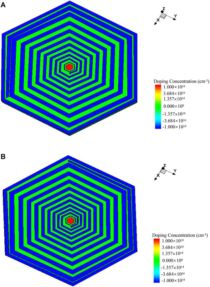
FIGURE 1. Front view of the detector. (A) First-order diagram; (B) second-order diagram.
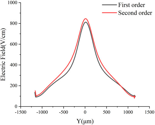
FIGURE 2. Electric field distribution of the one-dimensional cross-section of the detector (Z = −240 μm).
For a spiral at the radius as a function of the polar angle φ with a pitch p(r), we have
That is, as the polar angle increases by one full circle, the radius r increases by one pitch. The Taylor expansion is carried out to obtain the expansion formula to the second order:
First-order approximation:
where r (1) is the first-order radius and r(1)'(φ) is the first-order derivative of the relationship between the first-order radius and angle. Combining Eqs 1, 3, we obtain
By solving Eq. 4, we get
where r1 is the starting radius of the spiral ring, which is assumed to be 100 μm.
The second-order approximation is derived from Eqs 1, 2, and the first-order solution obtained from Eq. 5 is used to approximate the second derivative of r:
or
where r (2) is the second-order radius solution.
From Eq. 4, we have
By using Eq. 4, we have
or
By separating r and φ, we can get
Then, we can obtain
By replacing r(1) and r(2) on the right-hand side of Eq. 13 with r, we get
Finally, we get
We use a pitch function of the following form:
Hence,
where p1 is the initial pitch of the spiral rings, which is assumed 53 μm in this paper. We can rewrite Eq. 15 as follows:
We define, here,
Hence,
By taking derivatives from both sides, we get
By simplifying Eq. 21, we get
By combining Eqs 18, 19 and Eq. 22, we have
Further simplifying Eq. 23, we get
By carrying out integration, we obtain
By using Eq. 19, we have
Then, the first-order formula is deduced as follows:
Eq. 27 is further derived as follows:
Hence,
From Eq. 29, we can get the first-order radius formula as follows:
Similarly, the second-order radius formula can be derived from Eq. 26 as follows:
It should be noted here that on the right-hand side of Eq. 30, we used the known first-order solution value of radius. Then, we can use the iteration method to place the current solution value of radius on the right-hand side of Eq. 31 to get the next solution value of radius until the precision is to our satisfaction.
To further analyze the electrical performance of the first-order structure and the second-order structure of the spiral SDD, we used TCAD to simulate the first-order structure and the second-order structure of the detector, respectively. In order to analyze the internal characteristics of the detector, the following are further described from the aspects of electric field, potential, and electron concentration.
In this paper, the cross-sections of the first-order structure and the second-order structure of the detector are intercepted and compared to see the electric field distribution inside the detector and the difference between them more clearly. Figure 2 shows the cross-section of the detector (Z = −240 μm). It can be seen that the electric field distribution of the first- and second-order structures of the detector is relatively stable, but the electric field curve of the second-order structure is smoother and more uniform compared to the electric field curve of the first-order structure, and the electrical performance is more stable.
In order to more clearly highlight the first-order structure and the second-order structure of the detector, this paper is also presented in (Z = −240 μm) and compares and analyzes their potential diagrams. From Figure 3, we can see that the anode potential is the highest, then the potential gradually decreases with the increase in the radius. It is not difficult to see that the potential inside the second-order detector is more uniform and symmetrical than that of the first-order detector.
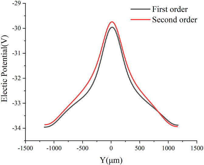
FIGURE 3. Potential distribution of the one-dimensional cross-section of the detector (Z = −240 μm).
Figure 4 shows the comparison of electron concentrations between the first order and the second order. The red area is the area with the highest concentration of electrons. This area is the drift orbit of electrons, and electrons will flow to the collecting anode along the drift channel. Although the concentration of electrons in this region is large, its concentration is always less than the doping concentration of the substrate itself, which indicates that the substrate has been fully depleted and this region is the drift channel for electrons with a finite drift field. The electrons outside the drift channel will first drift to the channel and then drift to the collection anode located in the center of the detector along this drift channel. It can be seen from the figure that the internal electron concentration distribution of the second-order structure detector is more uniform, and the channel is better defined and uniform.
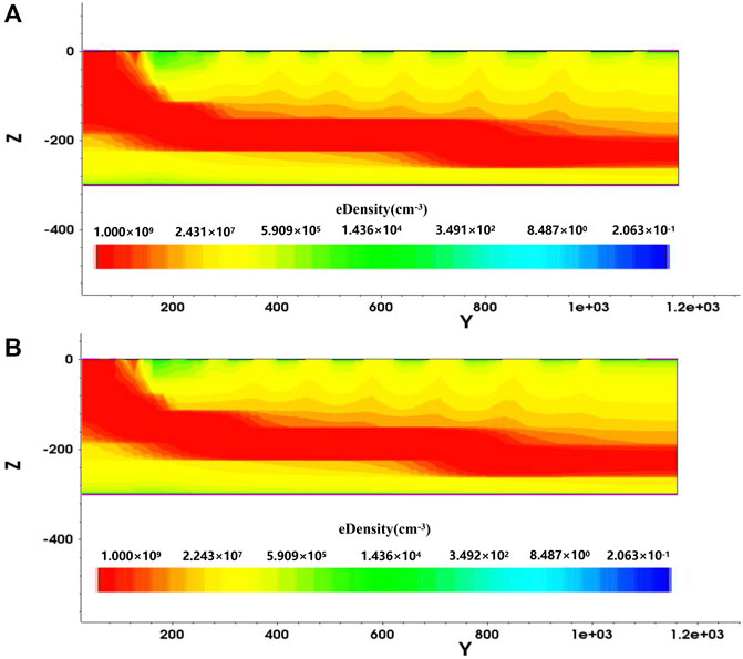
FIGURE 4. Distribution of the electron concentration of (A) first order and (B) second order inside the detector.
In this paper, we propose a calculation method for the spiral SDD with higher accuracy. The proposed new structure is more accurate than the previous one; the electric field distribution is more uniform, and the electronic drift channel inside the detector is clearer and more uniform. In this paper, we use TCAD to simulate the structure of the first- and second-order accuracy of the detector and compare the difference between the two detectors in terms of electric field, potential, and electron concentration. We determined that the second-order structure is more optimized and accurate than the original first-order structure. This research provides strong theoretical support for the production of detectors in the future.
The original contributions presented in the study are included in the article/supplementary material, further inquiries can be directed to the corresponding author.
XiaL and ZL contributed to conception and design of the study. JS, ZT, XC, and XinL organized the database. ML and HW performed the statistical analysis. XiaL wrote the first draft of the manuscript.
This study was supported by the Key Scientific and Technological Innovation Project of Shandong Province (Grant No. 2019TSLH0316) and Yantai City-University Integration Development Project (No. 2020XDRHXMP11).
The authors declare that the research was conducted in the absence of any commercial or financial relationships that could be construed as a potential conflict of interest.
All claims expressed in this article are solely those of the authors and do not necessarily represent those of their affiliated organizations, or those of the publisher, the editors, and the reviewers. Any product that may be evaluated in this article, or claim that may be made by its manufacturer, is not guaranteed or endorsed by the publisher.
Fiorini, C., Gola, A., Longoni, A., Zanchi, M., Restelli, A., Perotti, F., et al. (2006). A large-area monolithic array of silicon drift detectors for medical imaging. Nucl. Instrum. Methods Phys. Res. Sect. A Accel. Spectrom. Detect. Assoc. Equip. 568 (1), 96–100. doi:10.1016/j.nima.2006.07.025
Gatti, E., and Rehak, P. (1984). Semiconductor drift chamber — an application of a novel charge transport scheme. Nucl. Instrum. Methods Phys. Res. 225 (3), 608–614. doi:10.1016/0167-5087(84)90113-3
Guazzoni, C. (2010). The first 25 years of silicon drift detectors: A personal view. Nucl. Instrum. Methods Phys. Res. Sect. A Accel. Spectrom. Detect. Assoc. Equip. 624 (2), 247–254. doi:10.1016/j.nima.2010.06.005
Kalender, W. A., Kolditz, D., Steiding, C., Ruth, V., Luck, F., Rossler, A. C., et al. (2017). Technical feasibility proof for high-resolution low-dose photon-counting CT of the breast. Eur. Radiol. 27 (3), 1081–1086. doi:10.1007/s00330-016-4459-3
Li, X., Liu, M., and Li, Z. (2021). Design and simulation of silicon detector cells with spiral ring electrode structures. AIP Adv. 11 (4), 045127. doi:10.1063/5.0049765
Li, Z. (2013). Generalization of the modeling and design considerations of concentric and spiral Si drift detectors. Nucl. Instrum. Methods Phys. Res. Sect. A Accel. Spectrom. Detect. Assoc. Equip. 730, 73–78. doi:10.1016/j.nima.2013.06.066
Lindström, G., Moll, M., and Fretwurst, E. (1999). Radiation hardness of silicon detectors – A challenge from high-energy physics. Nucl. Instrum. Methods Phys. Res. Sect. A Accel. Spectrom. Detect. Assoc. Equip. 426 (1), 1–15. doi:10.1016/s0168-9002(98)01462-4
Liu, M., Li, Z., Deng, Z., He, L., Xiong, B., Li, Y., et al. (2021). 314 mm2 hexagonal double-sided spiral silicon drift detector for soft X-ray detection based on ultra-pure high resistance silicon. Front. Mater. 8. doi:10.3389/fmats.2021.700137
Lutz, G. (2003). Novel semiconductor detectors for X-ray astronomy and spectroscopy. Nucl. Instrum. Methods Phys. Res. Sect. A Accel. Spectrom. Detect. Assoc. Equip. 501 (1), 288–297. doi:10.1016/s0168-9002(02)02048-x
Moser, H.-G. (2009). Silicon detector systems in high energy physics. Prog. Part. Nucl. Phys. 63 (1), 186–237. doi:10.1016/j.ppnp.2008.12.002
Pourmorteza, A., Symons, R., Sandfort, V., Mallek, M., Fuld, M. K., Henderson, G., et al. (2016). Abdominal imaging with contrast-enhanced photon-counting CT: First human experience. Radiology 279 (1), 239–245. doi:10.1148/radiol.2016152601
Sun, J., Li, Z., Li, X., Li, X., Cai, X., Tan, Z., et al. (2022). Novel spiral silicon drift detector with equal cathode ring gap and given surface electric fields. Micromachines (Basel) 13 (10), 1682. doi:10.3390/mi13101682
Virdee, T. S. (2004). Detectors at LHC. Phys. Rep. 403-404, 401–434. doi:10.1016/j.physrep.2004.08.026
Witze, A. (2018). NASA test proves pulsars can function as a celestial GPS. Nature 553 (7688), 261–262. doi:10.1038/d41586-018-00478-8
Keywords: spiral silicon drift detector, second-order approximation, electric field distribution, potential distribution, electron concentration
Citation: Li X, Li Z, Sun J, Tan Z, Cai X, Li X, Liu M and Wang H (2023) Electrical properties of a high-precision hexagonal spiral silicon drift detector. Front. Mater. 10:1186668. doi: 10.3389/fmats.2023.1186668
Received: 15 March 2023; Accepted: 17 April 2023;
Published: 05 May 2023.
Edited by:
Ke Cao, Xidian University, ChinaCopyright © 2023 Li, Li, Sun, Tan, Cai, Li, Liu and Wang. This is an open-access article distributed under the terms of the Creative Commons Attribution License (CC BY). The use, distribution or reproduction in other forums is permitted, provided the original author(s) and the copyright owner(s) are credited and that the original publication in this journal is cited, in accordance with accepted academic practice. No use, distribution or reproduction is permitted which does not comply with these terms.
*Correspondence: Zheng Li, MzYzNkBsZHUuZWR1LmNu
Disclaimer: All claims expressed in this article are solely those of the authors and do not necessarily represent those of their affiliated organizations, or those of the publisher, the editors and the reviewers. Any product that may be evaluated in this article or claim that may be made by its manufacturer is not guaranteed or endorsed by the publisher.
Research integrity at Frontiers
Learn more about the work of our research integrity team to safeguard the quality of each article we publish.