 Carmen Rizzuto
 Riccardo C. Barberi
 Marco Castriota
94% of researchers rate our articles as excellent or good
Learn more about the work of our research integrity team to safeguard the quality of each article we publish.
Find out more
ORIGINAL RESEARCH article
Front. Mater., 18 July 2022
Sec. Smart Materials
Volume 9 - 2022 | https://doi.org/10.3389/fmats.2022.912013
In this work, WO3 and TiO2 thin films have been obtained by the sol-gel spin coating method. The as-deposited samples were annealed at different annealing temperatures in the range between 100°C and 500°C. Micro-Raman spectroscopy confirmed that WO3 thin films annealed at 100°C and 300°C are amorphous while the crystallization process occurred at 500°C as established by the typical Raman modes of γ-WO3. Amorphous thin films of TiO2 have been obtained using annealing at 100°C and 300°C. The crystalline phase of the anatase-TiO2 has been obtained after the thermal treatment conducted at 500°C. The electrochromic devices were characterized by cyclic voltammetry and UV–Vis–NIR spectroscopy and it has been shown that the best configurations of the electrochromic devices studied in this work can be obtained by using the WO3 thin films amorphous, which means annealed at 100°C and 300°C, and TiO2 thin films crystalline, that is annealed at 500°C. The higher coloration efficiency values in the visible region (λ = 550 nm) and in the near-infrared region (λ = 1020 nm) support the idea that such devices could be used in order to control the light flux but also heat flux. It means that such electrochromic devices can be usefully employed as smart windows promoting energy and economic savings.
Tungsten trioxide (WO3) and titanium dioxide (TiO2) thin films are promising layers to be used as electrodes in electrochromic devices and also in photochromic devices, chemical sensors, superconductors, and photocatalysts (Palgrave and Parkin, 2004; Wang et al., 2016; Yuksel et al., 2016; Tang et al., 1995; Karunagaran et al., 2007; Yu et al., 2001). Such layers can be obtained by different techniques such as sputtering, chemical or physics vapor deposition, sol-gel synthesis, and others. Among the different techniques, to obtain large-area electrodes, the sol-gel process results to be the best one because it can be done in a large tub, whereas the other techniques required that the substrates have to fit in a box chamber, usually with a controlled atmosphere. Moreover, the sol-gel synthesis allows obtaining transparent metal oxide thin films, with good homogeneity and optical properties also on different substrates including glass (Kim et al., 2002). Electrochromic devices exhibit low power consumption (Wen-Cheun Au et al., 2020; Wen-Cheun Au et al., 2019).
Amorphous-WO3, the working electrode in the electrochromic device, is a cathodic electrochemical material and it has specific optical properties that switch from transparent state to blue state (OFF/ON states) under double injection of ions and electrons under an applied voltage (Leftheriotis et al., 2007; Castriota et al., 2005; Patel et al., 2017). From a chemical point of view, the electrochromic coloring of tungsten trioxide is a synchronous uptake of electrons and ions into the film.
During this work, the counter electrode of the electrochromic device is made of titanium dioxide. Titanium dioxide (TiO2), the electrode is high transparent, with a high refractive index and chemical durability and is suitable in both visible and near-infrared regions. Various methods can be used for its synthesis including sol-gel, sputtering, chemical vapor deposition, e-beam evaporation processes application (Kim et al., 2002). The main phases of TiO2 are anatase (tetragonal), rutile (tetragonal), and brookite (orthorhombic) (Chrysicopoulou et al., 1998; Bakri et al., 2017). Titanium dioxide in anatase phase, for its physical-chemical properties, is generally favored when it is obtained by sol-gel process. Among the different metal oxide which can be used as a counter electrode, the titanium oxide electrode seems to increase the contrast of the electrochromic device.
The main aim of this work is to find the best thermal process to which to subject the metal oxide electrodes to make the electrochromic device with the best performance in terms of electro-optical properties and energy-saving promotion. Such aspects together with the use of the sol-gel synthesis could allow the scale-up of such technology and could have reals fallouts in the industrial environment with energy and economic benefits.
In this work, the sol-gel method has been used to obtain WO3 and TiO2 thin films which have been subjected to the annealing process at three temperatures (100°C, 300°C, and 500°C) for 1 h. After the annealing process, the working electrode (WO3) and the counter electrode (TiO2) have been assembled to obtain electrochromic devices made with electrodes annealed at different temperatures. The structural order and the thermodynamic phases, the electrochemical and optical properties of electrodes and devices have been studied by Raman spectroscopy, cyclic voltammetry, and UV–Vis–NIR spectroscopy, respectively. The physical chemistry properties shown by electrodes and electrochromic devices have been related to the annealing temperatures to which the metal oxide thin film has been subjected.
Tungsten (VI) oxychloride (WOCl4, 98% purity Aldrich), isopropanol anhydrous (99.5% purity), titanium (IV) isopropoxide (99,999% purity), and glacial acid acetic (99,99% purity) were purchased from Sigma-Aldrich Company. All the above-listed compounds were preserved inside the glove box, in an argon atmosphere, to avoid any reaction with moisture or oxygen present in the air. The other reagents such as polymethylmethacrylate, or PMMA (Mw = 120,000), lithium perchlorate (LiClO4), and propylene carbonate (PC), bisphenol-A glycerolate diacrylate (BA), and 2, 2-dimethoxy-2-phenyl acetophenone (Irgacure 651) were supplied by Sigma-Aldrich Company, too. BA was kept refrigerated. The used spacers of 200 μm of diameter were made by silica.
The tungsten trioxide mother solution was prepared in Ar atmosphere in a glove box (MBRAUN-Unilab) by dissolving tungsten (VI) oxychloride (WOCl4, 98% purity) in isopropanol anhydrous (99,5% purity). The WO3 mother solution was left to stir for 24 h and, then, deposited on indium tin oxide (ITO)-coated glass with spin coater (SC10 CaLCTec S.r.l.) at 1200 rpm for 30 s.
The titanium dioxide mother solution was prepared in an Ar atmosphere in a glove box (MBRAUN-Unilab) by dissolving titanium (IV) isopropoxide (Ti[OCH(CH3)2]4), 99,999% purity) in isopropanol anhydrous (99,5% purity Aldrich) and glacial acid acetic (99,99% purity, Aldrich). The TiO2 mother solution was stirred for 24 h and then deposited on indium tin oxide (ITO)-coated glass with spin coater (SC10 CaLCTec S.r.l.) at 1200 rpm for 30 s. The WO3 and TiO2 thin films obtained as said above have been annealed at 100°C, 300°C and 500°C for 1 h in air.
Electrochromic devices have been assembled by using the combination of WO3 and TiO2 electrodes annealed at 100°C, 300°C, and 500°C, in the followed sandwich configuration:
where glass-ITO is the transparent electrodes (TEs) used to apply the external voltage. The gel electrolyte has been made by dissolving polymethylmethacrylate, PMMA (Mw = 120,000, Sigma Aldrich), and LiClO4 (1M) in propylene carbonate (PC). Such gel has been injected by capillarity between the two electrodes. To prevent the short circuit of the systems, silica spacers of 200 μm diameter were introduced inside each device. All devices were sealed using an epoxydic resin composed of bisphenol-A glycerolate diacrylate and 2, 2-dimethoxy-2-phenyl acetophenone (Irgacure 651) as photo-initiator.
Raman spectra of WO3 and TiO2 thin films were collected by using a Jobin Yvon micro-Raman LABRAM equipped with a CCD (256 × 1,024 pixels) detector cooled at −70°C, an Nd:YAG (λ = 532 nm emission, 50 mW power) and a 50 X Olympus objective long working distance. The spectral resolution was 2 cm−1. All the Raman spectra have been collected at room temperature. WO3 representative Raman spectra have been collected range between 300 and 1400 cm−1 while the representative Raman spectra of TiO2 thin films have been collected in the range between 100 and 1,000 cm−1.
Cyclic voltammetry measurements were carried out on the electrochromic devices with a potentiostat/galvanostat, model 2059 low instrument interfaced with an Amel instrument-model 7800 interface (Amel Instruments). The tungsten trioxide electrode has been used as a working electrode in the electrochromic devices.
UV–Vis–NIR spectra have been collected by UV–Vis–NIR Spectrophotometer AvaSpec-2048-Avantes, in the range between 400 and 1200 nm. The equipment included also, a Deuterium-Halogen light source (DH-2000 UV–Vis–NIR Light source Avantes) and Agilent E3632A DC Power Supply (0–15 V, 7 A). Analyses were conducted at room temperature.
Raman spectroscopy has been used to study the effect of the annealing temperatures on the structural phases of the WO3 and TiO2 thin films. Figure 1 shows the representative Raman spectra collected on the tungsten trioxide thin films subjected, for 1 h, to three different annealing temperatures which are 100°C, 300°C, and 500°C. The as-deposited films contain some organic residues that are removed by the thermal treatments and, therefore, the metal oxide network is not completely done before the annealing process.
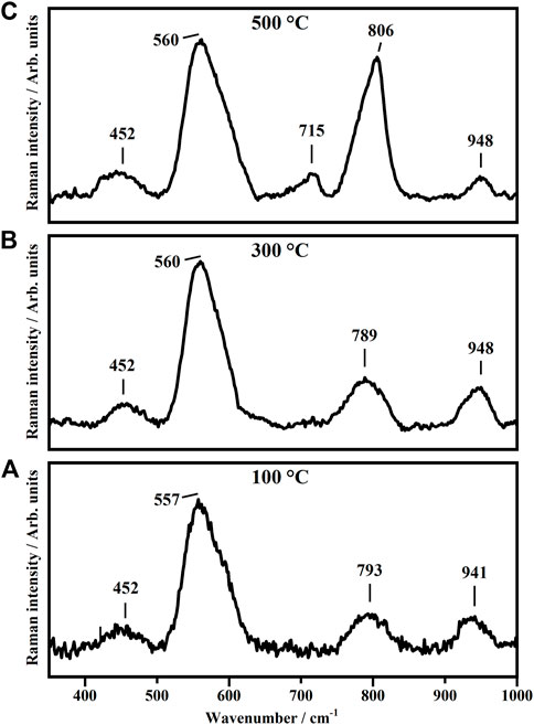
FIGURE 1. Representative Raman Spectra collected on WO3 thin films annealed, for 1 h, at 100°C (A), 300°C (B) and 500°C (C).
The Raman spectra collected on the tungsten trioxide thin film annealed for 1 h at 100°C (Figure 1A) show broad bands at about 793 and 941 cm−1 ascribed to the stretching modes W-O and terminal W=O bonds. The presence of such modes indicates that such films are in amorphous state (a-WO3) (Caruso et al., 2014). As it is possible to see in Figure 1B, the annealing treatment at 300°C does not change the structural phase of the tungsten trioxide thin film. In fact, the bands at 789 and 948 cm−1 (Figure 1B) are still due to the stretching modes W-O and terminal W=O bonds confirming that such films are in amorphous state (a-WO3) (Caruso et al., 2014). A great effect on the structural phase of the tungsten trioxide thin films has been obtained when the as-deposited thin films were subjected to the highest annealing temperature, 500°C (Figure 1C). The two bands at 715 and 806 cm−1 shown in the representative Raman spectra of Figure 1C are due to the presence of crystalline tungsten trioxide and in particular of γ-monoclinic phase (γ-WO3) (Cazzanelli et al., 1999a; Kuzmin et al., 1998). In this case, the band at 788 cm−1 above assigned to the stretching mode of W-O bonds results to be split into two components at 715 and 806 cm−1 ascribed to the O-W-O stretching modes of the bridging oxygen in WO3. The other Raman modes that fall at about 452 cm−1 and 560 cm−1 detected on all the samples have been ascribed to the ITO-glass substrates, where the tungsten trioxide thin films have been deposited.
The representative Raman spectra collected on TiO2 thin films annealed, for 1 h, at 100°C, 300°C and 500°C are shown in Figure 2.
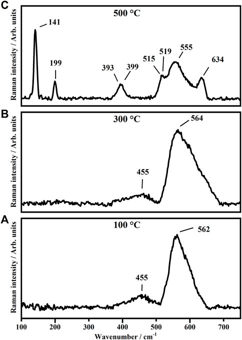
FIGURE 2. Representative Raman Spectra collected on TiO2 thin films annealed, for 1 h, at 100°C (A), 300°C (B) and 500°C (C).
As shown in Figure 2, the Raman spectra collected on the titanium dioxide thin films annealed at 100°C and 300°C do not show any detectable Raman features ascribable to the titanium dioxide thin films. The only modes at about 455, 562, and 564 are assigned to the glass substrates. The no detectability of Raman features of the TiO2 is due to the very low Raman cross-section of the amorphous phases with respect to the crystalline ones. In fact, the as-deposited samples annealed at 500°C, as shown in Figure 2C , show Raman peaks, some of them quite sharp representative of the crystalline phases. The Raman peaks at 141, 199, 393, 399, 515, 519, and 634 cm−1 are assigned to TiO2 in the anatase phase in its tetragonal coordination with space group D19 (An-TiO2). In particular, the peaks at 141 and 199 cm−1 are due to the Eg modes, the peaks at 393 and 399 cm−1 are representative of the B1g mode. The Raman bands at 515 and 519 cm−1 are attributed to the A1g and B1g vibrational modes and the peak at 634 cm−1 is assigned to the Eg vibrational mode (Karunagaran et al., 2005). The peak at 555cm−1 is ascribed to the glass substrate (Djaoued et al., 2012; Daniel et al., 1987; Gotić et al., 2000; Cazzanelli et al., 1999b; Ohsaka et al., 1978; Balaji et al., 2009; Balachandran and Eror, 1982; Rezaee et al., 2011; Yazid et al., 2018; Alam and Cameron, 2002; Dinh et al., 2003; Judeinstein et al., 1992; Huang et al., 1997).
Cyclic voltammetry has been performed to investigate the reversibility of the electrochromic behavior, the cathodic and anodic current peaks and how those could be related to the annealing temperature of the WO3 and TiO2 electrodes used to build the electrochromic devices. (The electrochromic device studied will be indicated as WxTiy where W and Ti indicate the WO3 and TiO2 electrodes, respectively; indeed, the subscripts x and y indicate the annealing temperature expressed in hundreds of the WO3 and TiO2 electrodes, respectively.) Of course, since the WO3 and TiO2 electrodes have been annealed at three different temperatures each, then the possible combinations of them to make electrochromic devices are nine. The voltammograms acquired on the nine kinds of electrochromic devices with scan rate of 50 mV/s and after five cycles are shown in Figure 3.
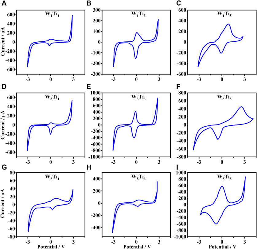
FIGURE 3. Cyclic voltammetry from −3.5 to 3.5 V (scan rate of 50 mV/s) of the nine following electrochromic devices: (A) W1Ti1, (B) W1Ti3, (C) W1Ti5, (D) W3Ti1, (E) W3Ti3, (F) W3Ti5, (G) W5Ti1, (H) W5Ti3 and (I) W5Ti5. (WxTiy where W and Ti indicate the WO3 and TiO2 electrodes, respectively and the subscripts x and y indicate their annealing temperature expressed in hundreds, respectively.)
As shown in Figure 3, the nine kinds of electrochromic devices assembled show similar electrochemical behavior during cyclic voltammetry investigation. Both the electrodes, WO3 and TiO2, are cathodic electrochromic materials: become colored for negative applied voltage when the lithium ions dissolved in the polymeric gel are inserted in the metal oxide layer. This insertion is associated with a reduction reaction of the oxidation state of the metal. In Eqs 1 and 2 are reported the reactions of the WO3 and TiO2, electrodes used in the studied electrochromic devices (Granqvist, 1995):
In the beginning, each system was colorless and the devices become blue during the negative potential cycle and bleaching during the positive potential cycle. As described in Eq. 1, the coloration is associated with the simultaneous and reversible injection of lithium cations and electrons inside the oxide network and it is due to the reduction process which promotes the formation of tungsten atoms in a reduced oxidation state (W(V)) which are responsible for the blue color of the films. In this electrochromic device, the titanium dioxide works as described in Eq. 2 but since its change of color it is not appreciable its function is of the ions storage. In such a way, when the electrochromic devices are blue, it means that Eq. 1 it is shifted on the right while Eq. 2 it is shifted on the left: state ON. When the devices are transparent then Eq. 1 it is shifted on the left while Eq. 2 it is shifted on the right: state OFF.
As shown in Figure 3, not all voltammograms show the same profile and some of the results are deformed and shifted with respect to the center. Such differences in cyclic voltammetry curves could be due to different ion migrations and electron trapping/de-trapping, at the interface of the metal-oxide thin film and gel electrolyte, in the redox process (Heckner and Kraft, 2002), the possible degradation of gel electrolyte subjected to an external applied voltage and the probable presence of some impurities as, for example, water. Nevertheless, the specific cathodic potentials which turn ON the electrochromic devices have been collected and are summarized in Table 1.

TABLE 1. Cathodic potentials which turn ON the following electrochromic devices: a) W1Ti1, b) W1Ti3, c) W1Ti5, d) W3Ti1, e) W3Ti3, f) W3Ti5, g) W5Ti1, h) W5Ti3 and i) W5Ti5. (WxTiy where W and Ti indicate the WO3 and TiO2 electrodes, respectively and the subscripts x and y indicate their annealing temperature expressed in hundreds, respectively) (see Figure 3).
The different values of potentials observed are ascribed to the different order degree (phase), due to the different annealing processes, which the working electrode (WO3) and counter electrode (TiO2) used to build the nine electrochromic devices studied were subjected.
As it is possible to see from Table 1, the highest absolute value of the cathodic potentials which turn ON the electrochromic device is that of the W5Ti5 electrochromic device which is made by using WO3 and TiO2 electrodes annealed at the highest temperature (500°C) which induces the transformation of the amorphous films in crystalline films, which show a prevalent electronic conduction with respect to the ionic conduction. It means that the ionic conductivity responsible for the insertion reaction at the basis of the electrochromic effect is disadvantaged and for this reason, it is needed a higher potential for switching ON the working electrode.
It fit very well with the coloring process described above where the WO3 layer becomes blue after the insertion of the lithium ions which is favored in systems with prevalent ionic conductivity as the amorphous state with respect to the crystalline ones.
UV–Vis–NIR spectroscopy has been performed on the electrochromic devices made, as mentioned above, with WO3 and TiO2 thin films annealed at different temperatures (100°C, 300°C and 500°C) to study the optical properties of such devices and their energy-saving applications on buildings.
The transmittance modulation (%) of each electrochromic device was monitored at fixed potential values equal to 0 V, −1.6 V, −1.8 V, −2 V and −2.8 V in the wavelength region from 400 to 1200 nm when the systems are put in the condition of bleached state (state OFF) and in the colored state (state ON). The transmittance curves of all electrochromic devices are shown in Figure 4.
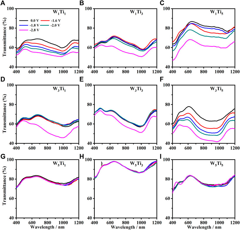
FIGURE 4. Optical transmittance curves, in the range between 400 and 1200 nm, of the nine following electrochromic devices: (A) W1Ti1, (B) W1Ti3, (C) W1Ti5, (D) W3Ti1, (E) W3Ti3, (F) W3Ti5, (G) W5Ti1, (H) W5Ti3 and (I) W5Ti5. (WxTiy where W and Ti indicate the WO3 and TiO2 electrodes, respectively and the subscripts x and y indicate their annealing temperature expressed in hundreds, respectively.) The black line corresponds to the 0.0 V (no voltage applied, state OFF). The red, blue, green and magenta lines correspond to the following states ON at −1.6 V, −1.8 V, −2.0 V and −2.8 V applied voltage, respectively.
As it is possible to see in Figure 4, not all nine kinds of the electrochromic devices show the same behavior of the optical transmittance. In particular, it is possible to see that the transmittance curves of the electrochromic devices made with WO3 films annealed at 500°C (W5Ti1, W5Ti3, and W5Ti5) seems do not change under the action of the applied voltage used during this work: all the optical transmittance curve, collected at a different voltage, are the same of the curve collected when no voltage is applied and are superposed (Figures 4G–I). This behavior is in agreement with the previous considerations about the nature of the WO3 annealed at 500°C, which results to be crystalline with a prevalent electronic conduction, which disadvantages the electrochromic effect due to the insertion of the small lithium ions in the WO3 lattice. The transmittance curves of the following electrochromic devices, W1Ti1, W1Ti3, W3Ti1, and W3Ti3 show a detectable change of the transmittance curve just when the devices are subjected to the highest (in absolute value) (−2.8 V) applied voltage (Figures 4B,D,E). It can be explained just considering that the amount of the lithium ions inserted in the WO3 layer for applied voltage lower than −2.8 V (in absolute value) is not enough to switch ON the electrochromic devices. A very interesting decrease of the transmittance curves as a function of the applied voltage has been seen for the following electrochromic devices: W1Ti1, W1Ti5, and W3Ti5. The transmittance curves of the W1Ti1 device are almost close to each other while the curves collected on the other two devices, W1Ti5 and W3Ti5, are quite far from each other and so they can offer a bigger change in the transmittance when the device is switched ON. Therefore, the devices which show the maximum change of the transmittance are those made with WO3 electrode annealed at lower temperatures (100°C and 300°C) which let the layer in amorphous state with prevalent ionic conduction, with respect to the electronic conduction, that promote the electrochromic effect and the TiO2 film annealed at 500°C that are quite crystalline with a prevalent electronic conduction with respect to the ionic conduction, that supports the electrochromic effect by the electrons injection in the WO3 films to balance the lithium ions inserted.
In order to give a quantitative estimation of the efficiency electrochromic devices made during this work, it has determined the coloration efficiency (CE) of each device. The CE is defined as the change in optical density ΔOD at a particular wavelength (λ) per unit area (S) of charge (Q) intercalated or extracted from the electrochromic film. It can be calculated according to the following (Eq. 3) (Monk et al., 1995; Patel et al., 2009; Ren et al., 2015):
where TOFF and TON represent the transmittance in the OFF state (bleached) and ON state (colored).
The state OFF corresponds to the absence of applied voltage whereas the state is ON when the electrochromic device is subjected to the applied voltage equal to −2.8 V.
In order to evaluate the response of the electrochromic device in the visible range and in the NIR range the CE have been calculated at two wavelengths: 550 and 1020 nm. All the data and the results are summarized in Table 2.
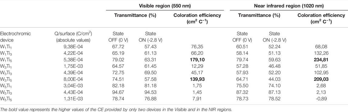
TABLE 2. Transmittances of the states Off (0.0 V) and On (−2.8 V) and coloration efficiency values in the visible region (λ = 550 nm) and Near Infrared region (λ = 1020 nm) of the following electrochromic devices: W1Ti1, W1Ti3, W1Ti5, W3Ti1, W3Ti3, W3Ti5, W5Ti1, W5Ti3, and W5Ti5 (WxTiy, where W and Ti indicate the WO3 and TiO2 electrodes, respectively and the subscripts x and y indicate their annealing temperature expressed in hundreds, respectively) (see Figure 4).
The CE values estimations confirm quantitatively what has been stated above qualitatively. In fact, as it is possible to see in Table 2, in the visible region the higher CE values, 179.10 and 139.93 cm2 C−1, are obtained for the W1Ti5 and W3Ti5 devices. Also in the near-infrared region the higher CE value, 234.81 and 209.03 cm2 C−1 are obtained for the W1Ti5 and W3Ti5 devices. Both the kinds of electrochromic devices are made by using amorphous WO3 and crystalline TiO2 electrodes, that as said above, represent the best device configurations studied during this work. The electrochromic devices made during this work, show values of CE quite competitive with respect to those obtained from systems described in the previous literature in which the optical properties are improved by common strategies such as metal oxide doping (Cai et al., 2013; Yun et al., 2019), composite formation (Prasad et al., 2022), and nanostructuring (Eyovge et al., 2021). Therefore, ours electrochromic devices are quite promising to be used as smart windows in saving energy applications.
In this work, electrochromic devices made by using as electrodes WO3 and TiO2 layers, obtained by sol-gel synthesis and annealed at three different temperatures (100°C, 300°C, and 500°C), have been studied. The WO3 and TiO2 thin films annealed at 100°C, 300°C, and 500°C have been investigated by Raman spectroscopy and it has been shown that both the metal oxide thin films are amorphous when subjected to the annealed temperatures at 100°C and 300°C whereas they become crystalline when treated at 500°C annealed temperature. The structural order of the metal oxide films is quite important because it is well known (Marino et al., 2005; Bruno et al., 2005; Castriota et al., 2014) that amorphous metal oxide thin films are better ionic conductors than electronic conductors while crystalline thin films show an opposite behavior; in fact, crystalline thin films are better electronics conductors than ionic conductor.
Such findings have been very useful to explain the voltammogram obtained on the nine kinds of electrochromic devices that are studied. The devices become colored when the lithium injection occurs in the WO3 lattice and this is favored in amorphous films where, the ionic conductivity is highest while, the highest cathodic potential (the potential at which the electrochromic devices begin to turn ON) has been obtained with WO3 and TiO2 thin films annealed at 500°C, which are both in crystalline states. The UV–Vis–NIR analysis has confirmed that the best configurations of the electrochromic devices studied in this work can be obtained by using the WO3 thin films amorphous, that means annealed at 100°C and 300°C, and TiO2 thin films crystalline, that is annealed at 500°C.
The higher CE values in the visible region (λ = 550 nm) and in the near-infrared region (λ = 1020 nm) support the idea that such devices could be used in order to control the light flux but also the heat flux and so, those devices could be used for energy-saving applications (Castriota et al., 2013).
In the near future, the chance to integrate the electrochromic device with photovoltaic technology seems to be quite promising for many different industrial applications, since, in this way, the voltage needed to turn ON/OFF the electrochromic device can be given by the photovoltaic device.
The original contributions presented in the study are included in the article/Supplementary Material, and further inquiries can be directed to the corresponding author.
CR developed the methodology preparation, collected the characterization data and dispose the draft of the article. RB supervised the main idea of the study, reviewed the manuscript and he is acknowledged for its financial contribution. MC conceived and supervised the main idea of the study, wrote, reviewed, and edited the manuscript. He is acknowledged for its financial contribution. All authors have read and agreed to the published version of the manuscript.
We thank POR CALABRIA FESR-FSE 2014-2020-ASSE I—PROMOZIONEDELLA RICERCA E DELL’INNOVAZIONE Obiettivo specifico 1.2 Azione 1.2.2′ Project: “MERAVIGLIE.” This work was supported by the following projects: PON ARS01_00401-DEMETRA, CUP: B24I20000080001.
The authors declare that the research was conducted in the absence of any commercial or financial relationships that could be construed as a potential conflict of interest.
All claims expressed in this article are solely those of the authors and do not necessarily represent those of their affiliated organizations, or those of the publisher, the editors and the reviewers. Any product that may be evaluated in this article, or claim that may be made by its manufacturer, is not guaranteed or endorsed by the publisher.
MC and CR.would like to thank Prof. Enzo Cazzanelli for useful discussions.
Alam, M. J., and Cameron, D. C. (2002). Preparation and Characterization of TiO2 Thin Films by Sol-Gel Method. J. Sol-Gel Sci. Technol. 25, 137–145. doi:10.1023/A:1019912312654
Bakri, A. S., Sahdan, M. Z., Adriyanto, F., Raship, N. A., Said, N. D. M., Abdullah, S. A., et al. (2017). Effect of Annealing Temperature of Titanium Dioxide Thin Films on Structural and Electrical Properties. AIP Conf. Proc. 1788, 030030. doi:10.1063/1.4968283
Balachandran, U., and Eror, N. G. (1982). Raman Spectra of Titanium Dioxide. J. Solid State Chem. 42, 276–282. doi:10.1016/0022-4596(82)90006-8
Balaji, S., Albert, A.-S., Djaoued, Y., and Brüning, R. (2009). Micro-Raman Spectroscopic Characterization of a Tunable Electrochromic Device for Application in Smart Windows. J. Raman Spectrosc. 40, 92–100. doi:10.1002/jrs.2086
Bruno, V., Castriota, M., Marino, S., Versace, C., Strangi, G., Cazzanelli, E., et al. (2005). Asymmetric Response to Electric Field in Nematic Liquid Crystal Cells Containing Vanadium Oxide Thin Films Prepared by Sol-Gel Synthesis. Mol. Cryst. Liq. Cryst. 441, 27–43. doi:10.1080/154214091009527
Cai, G. F., Wang, X. L., Zhou, D., Zhang, J. H., Xiong, Q. Q., Gu, C. D., et al. (2013). Hierarchical Structure Ti-Doped WO3 Film with Improved Electrochromism in Visible-Infrared Region. RSC Adv. 3, 6896. doi:10.1039/c3ra40675j
Caruso, T., Castriota, M., Policicchio, A., Fasanella, A., De Santo, M. P., Ciuchi, F., et al. (2014). Thermally Induced Evolution of Sol-Gel Grown WO3 Films on ITO/glass Substrates. Appl. Surf. Sci. 297, 195–204. doi:10.1016/j.apsusc.2014.01.154
Castriota, M., Cazzanelli, E., De Santo, G., La Deda, M., and Termine, R., 2013. 1. WO2013054367 - ELECTROCHROMIC DEVICE. PCT/IT2012/000309-WO2013054367.
Castriota, M., Cazzanelli, E., Fasanella, A., and Teeters, D. (2014). Electrical Conductivity and Raman Characterization of V2O5 Grown by Sol-Gel Technique inside Nanoscale Pores. Thin Solid Films 553, 127–131. doi:10.1016/j.tsf.2013.11.126
Castriota, M., Marino, S., Versace, C., Strangi, G., Scaramuzza, N., and Cazzanelli, E. (2005). Characterization of Tungsten Trioxide Thin Film Deposited by Spin Coating and the Effect on Their Insertion in Liquid Crystal Cells. Mol. Cryst. Liq. Cryst. 429, 237–253. doi:10.1080/15421400590930980
Cazzanelli, E., Vinegoni, C., Mariotto, G., Kuzmin, A., and Purans, J. (1999a). Low-Temperature Polymorphism in Tungsten Trioxide Powders and its Dependence on Mechanical Treatments. J. Solid State Chem. 143, 24–32. doi:10.1006/jssc.1998.8061
Cazzanelli, E., Vinegoni, C., Mariotto, G., Kuzmin, A., and Purans, J. (1999b). Raman Study of the Phase Transitions Sequence in Pure WO3 at High Temperature and in HxWO3 with Variable Hydrogen Content. Solid State Ion. 123, 67–74. doi:10.1016/S0167-2738(99)00101-0
Chrysicopoulou, P., Davazoglou, D., Trapalis, C., and Kordas, G. (1998). Optical Properties of Very Thin (. Thin Solid Films 323, 188–193. doi:10.1016/S0040-6090(97)01018-3
Daniel, M. F., Desbat, B., Lassegues, J. C., Gerand, B., and Figlarz, M. (1987). Infrared and Raman Study of WO3 Tungsten Trioxides and WO3, xH2O Tungsten Trioxide Tydrates. J. Solid State Chem. 67, 235–247. doi:10.1016/0022-4596(87)90359-8
Dinh, N. N., Oanh, N. T. T., Long, P. D., Bernard, M. C., and Hugot-Le Goff, A. (2003). Electrochromic Properties of TiO2 Anatase Thin Films Prepared by a Dipping Sol-Gel Method. Thin Solid Films 423, 70–76. doi:10.1016/S0040-6090(02)00948-3
Djaoued, Y., Balaji, S., and Brüning, R. (2012). Electrochromic Devices Based on Porous Tungsten Oxide Thin Films. J. Nanomater. 2012, 1–9. doi:10.1155/2012/674168
Eyovge, C., Deenen, C. S., Ruiz-Zepeda, F., Bartling, S., Smirnov, Y., Morales-Masis, M., et al. (2021). Color Tuning of Electrochromic TiO2 Nanofibrous Layers Loaded with Metal and Metal Oxide Nanoparticles for Smart Colored Windows. ACS Appl. Nano Mat. 4, 8600–8610. doi:10.1021/acsanm.1c02231
Gotić, M., Ivanda, M., Popović, S., and Musić, S. (2000). Synthesis of Tungsten Trioxide Hydrates and Their Structural Properties. Mat. Sci. Eng. B 77, 193–201. doi:10.1016/S0921-5107(00)00488-8
Heckner, K., and Kraft, A. (2002). Similarities between Electrochromic Windows and Thin Film Batteries. Solid State Ionics 152-153 (153), 899–905. doi:10.1016/S0167-2738(02)00446-0
Huang, P. J., Chang, H., Yeh, C. T., and Tsai, C. W. (1997). Phase Transformation of TiO2 Monitored by Thermo-Raman Spectroscopy with TGA/DTA. Thermochim. Acta 297, 85–92. doi:10.1016/S0040-6031(97)00168-8
Judeinstein, P., Morineau, R., and Livage, J. (1992). Electrochemical Degradation of WO3·nH2O Thin Films. Solid State Ionics 51, 239–247. doi:10.1016/0167-2738(92)90206-5
Karunagaran, B., Kim, K., Mangalaraj, D., Yi, J., and Velumani, S. (2005). Structural, Optical and Raman Scattering Studies on DC Magnetron Sputtered Titanium Dioxide Thin Films. Sol. Energy Mater. Sol. Cells 88, 199–208. doi:10.1016/j.solmat.2004.03.008
Karunagaran, B., Uthirakumar, P., Chung, S. J., Velumani, S., and Suh, E.-K. (2007). TiO2 Thin Film Gas Sensor for Monitoring Ammonia. Mater. Charact. 58, 680–684. doi:10.1016/j.matchar.2006.11.007
Kim, D. J., Hahn, S. H., Oh, S. H., and Kim, E. J. (2002). Influence of Calcination Temperature on Structural and Optical Properties of TiO2 Thin Films Prepared by Sol-Gel Dip Coating. Mater. Lett. 57, 355–360. doi:10.1016/S0167-577X(02)00790-5
Kuzmin, A., Purans, J., Cazzanelli, E., Vinegoni, C., and Mariotto, G. (1998). X-Ray Diffraction, Extended X-Ray Absorption Fine Structure and Raman Spectroscopy Studies of WO3 Powders and (1−x)WO3−y⋅xReO2 Mixtures. J. Appl. Phys. 84, 5515–5524. doi:10.1063/1.368596
Leftheriotis, G., Papaefthimiou, S., and Yianoulis, P. (2007). Dependence of the Estimated Diffusion Coefficient of LixWO3 Films on the Scan Rate of Cyclic Voltammetry Experiments. Solid State Ionics 178, 259–263. doi:10.1016/j.ssi.2006.12.019
Marino, S., Castriota, M., Bruno, V., Cazzanelli, E., Strangi, G., Versace, C., et al. (2005). Changes of the Electro-Optic Response of Nematic Liquid Crystal Cells Due to Inserted Titania-Vanadia Films. J. Appl. Phys. 97, 013523. doi:10.1063/1.1826218
Monk, P. M. S., Mortimer, R. J., and Rosseinsky, D. R. (1995). Electrochromism: Fundamentals and Applications. Weinheim New York: VCH.
Ohsaka, T., Izumi, F., and Fujiki, Y. (1978). Raman Spectrum of Anatase, TiO2. J. Raman Spectrosc. 7, 321–324. doi:10.1002/jrs.1250070606
Palgrave, R. G., and Parkin, I. P. (2004). Aerosol Assisted Chemical Vapour Deposition of Photochromic Tungsten Oxide and Doped Tungsten Oxide Thin Films. J. Mat. Chem. 14, 2864–2867. doi:10.1039/B406337F
Patel, K. J., Bhatt, G. G., Bhatt, G. G., Patel, S. S., Desai, R. R., Ray, J. R., et al. (2017). Thickness-dependent Electrochromic Properties of Amorphous Tungsten Trioxide Thin Films. J. Nano- Electron. Phys. 9, 03040–03041–03040–4. doi:10.21272/jnep.9(3).03040
Patel, K. J., Panchal, C. J., Kheraj, V. A., and Desai, M. S. (2009). Growth, Structural, Electrical and Optical Properties of the Thermally Evaporated Tungsten Trioxide (WO3) Thin Films. Mater. Chem. Phys. 114, 475–478. doi:10.1016/j.matchemphys.2008.09.071
Prasad, A. K., Park, J.-Y., Kang, S.-H., and Ahn, K.-S. (2022). Electrochemically Co-deposited WO3-V2o5 Composites for Electrochromic Energy Storage Applications. Electrochimica Acta 422, 140340. doi:10.1016/j.electacta.2022.140340
Ren, Y., Gao, Y., and Zhao, G. (2015). Facile Single-step Fabrications of Electrochromic WO3 Micro-patterned Films Using the Novel Photosensitive Sol-Gel Method. Ceram. Int. 41, 403–408. doi:10.1016/j.ceramint.2014.08.084
Rezaee, M., Mousavi Khoie, S. M., and Liu, K. H. (2011). The Role of Brookite in Mechanical Activation of Anatase-To-Rutile Transformation of Nanocrystalline TiO2: An XRD and Raman Spectroscopy Investigation. CrystEngComm 13, 5055–5061. doi:10.1039/C1CE05185G
Tang, H., Prasad, K., Sanjinés, R., and Lévy, F. (1995). TiO2 Anatase Thin Films as Gas Sensors. Sensors Actuators B Chem. 26, 71–75. doi:10.1016/0925-4005(94)01559-Z
Wang, Y., Cui, X., Yang, Q., Liu, J., Gao, Y., Sun, P., et al. (2016). Preparation of Ag-Loaded Mesoporous WO3 and its Enhanced NO2 Sensing Performance. Sensors Actuators B Chem. 225, 544–552. doi:10.1016/j.snb.2015.11.065
Wen-Cheun Au, B., Chan, K.-Y., and Knipp, D. (2019). Effect of Film Thickness on Electrochromic Performance of Sol-Gel Deposited Tungsten Oxide (WO3). Opt. Mater. 94, 387–392. doi:10.1016/j.optmat.2019.05.051
Wen-Cheun Au, B., Tamang, A., Knipp, D., and Chan, K.-Y. (2020). Post-annealing Effect on the Electrochromic Properties of WO3 Films. Opt. Mater. 108, 110426. doi:10.1016/j.optmat.2020.110426
Yazid, S. A., Rosli, Z. M., Juoi, J. M., and Johari, N. D. (2018). Raman Spectroscopy and XRD Investigation on TiO2 Sol-Gel Dip Coating Thin Films Synthesizes with and without Solvents. MATEC Web Conf. 150, 04007. doi:10.1051/matecconf/201815004007
Yu, J., Zhao, X., and Zhao, Q. (2001). Photocatalytic Activity of Nanometer TiO2 Thin Films Prepared by the Sol-Gel Method. Mater. Chem. Phys. 69, 25–29. doi:10.1016/S0254-0584(00)00291-1
Yuksel, R., Durucan, C., and Unalan, H. E. (2016). Ternary Nanocomposite SWNT/WO 3/PANI Thin Film Electrodes for Supercapacitors. J. Alloys Compd. 658, 183–189. doi:10.1016/j.jallcom.2015.10.216
Keywords: Tungsten oxide, titanium oxide, sol gel synthesis, thin films, electrochromic device, Raman spectroscopy, cyclic voltammetry, UV–Vis–NIR spectroscopy
Citation: Rizzuto C, Barberi RC and Castriota M (2022) Tungsten and Titanium Oxide Thin Films Obtained by the Sol-Gel Process as Electrodes in Electrochromic Devices. Front. Mater. 9:912013. doi: 10.3389/fmats.2022.912013
Received: 03 April 2022; Accepted: 03 June 2022;
Published: 18 July 2022.
Edited by:
Amerigo Beneduci, University of Calabria, ItalyReviewed by:
Yang Zhao, Western University, CanadaCopyright © 2022 Rizzuto, Barberi and Castriota. This is an open-access article distributed under the terms of the Creative Commons Attribution License (CC BY). The use, distribution or reproduction in other forums is permitted, provided the original author(s) and the copyright owner(s) are credited and that the original publication in this journal is cited, in accordance with accepted academic practice. No use, distribution or reproduction is permitted which does not comply with these terms.
*Correspondence: Marco Castriota, bWFyY28uY2FzdHJpb3RhQGZpcy51bmljYWwuaXQ=
Disclaimer: All claims expressed in this article are solely those of the authors and do not necessarily represent those of their affiliated organizations, or those of the publisher, the editors and the reviewers. Any product that may be evaluated in this article or claim that may be made by its manufacturer is not guaranteed or endorsed by the publisher.
Research integrity at Frontiers
Learn more about the work of our research integrity team to safeguard the quality of each article we publish.