 Zhang Lei1
 Pan Hongyu
- 1College of Energy Engineering, Xi’an University of Science and Technology, Xi’an, China
- 2School of Safety Science and Engineering, Xi’an University of Science and Technology, Xi’an, China
Herein, we report a novel solvent-induced fabrication method to synthesize a perovskite thin film on flexible substrates. The high-quality CH3NH3PbI3 (MAPbI3) thin film is successfully fabricated, which is applied to prepare the stable flexible photodetector (PD). Compared with the reported results, this method achieved a low-temperature and low-cost perovskite thin film fabrication process on a flexible substrate. The constructed MAPbI3 layer possesses the advantages of being highly crystalline, uniform, and compact in a large area. The flexible PD based on the as-prepared perovskite thin film exhibits excellent performance and long-term stability. The EQE and R of the flexible PDs reached 8 × 10²% and 3.6 A/W, respectively. At the same time, the flexible PDs still showed superior stability and high performance after 15 days of continuous working. The presented high-quality perovskite thin-film fabrication method and high-performance flexible perovskite PDs are expected for application in the development of novel optoelectronic devices.
1 Introduction
Opto-electronic devices constructed on flexible substrates are emerging in different areas, including industry, military, and research. Their applications, such as portable display, sensor, detector, and solar cell, have been extensively explored. The advantages of high mechanical, flexibility, lightweight, and low manufactured temperature are preferable for advanced portable and wearable electronic equipment (Hamers, 2001; Park et al., 2012; Zheng et al., 2017). A photodetector (PD) is an important opto-electronic device for detecting optical signals and converting them into electrical ones (Sze et al., 1971; Dou et al., 2014; Alwadai et al., 2017; Bai et al., 2018). For decades, flexible PDs have attracted considerable attention owing to their enormous commercial applications. Unfortunately, the poor device performance and high working voltage remain to be figured out in order to realize their practical application in low-cost and flexible opto-electronic systems (Park et al., 2012).
Recently, a new group of organic-inorganic halide perovskite (OIHP) materials are demonstrated to be a class of excellent semiconductors. The OIHPs own outstanding optical and electronic performance characteristics, such as direct bandgap, high light absorption coefficient, and excellent charge carrier transport properties (Kojima et al., 2009; Lee et al., 2012; Yamada et al., 2014; Zhou et al., 2014; Li et al., 2019). Obviously, the OIHP-based photovoltaic cells show advanced rapid power conversion efficiency and reach the highest value of over 25% so far (Dong et al., 2015; Saidaminov et al., 2016; Lin et al., 2017). The perovskite materials have also been investigated in other opto-electronic devices of light-emitting diodes, lasers, and PDs (Caldeira Filho and Mulato, 2011; Xia et al., 2014; Lian, 2015; Kang, 2016; Manser et al., 2016; Wang et al., 2016; Hu et al., 2017; Hu et al., 2019; Mujahid et al., 2020; Shao and Hu, 2020; Mei et al., 2021).
Based on the reported results so far, the flexible perovskite devices have relatively lower performance than the devices on rigid wafers. One of the key shortcomings is that a compact and large-area high-quality perovskite active layer cannot be effectively constructed on flexible substrates. In order to obtain a high-quality material, herein, solvent engineering is introduced in this work. The manufacturing process is performed on a bendable poly(ethylene terephthalate) (PET) substrate. The perovskite thin film, achieved by the novel solvent-induced method, shows combination properties, namely, highly compact and crystalline. Using the as-grown perovskite film, a metal–semiconductor–metal PD has also been successfully constructed. The resulting PD exhibits enhanced performance of higher performance and lower working voltage which achieves a maximum external quantum efficiency (EQE) of 8 × 10²% and a responsivity (R) of 3.7 A/W at a low bias of 1 V, respectively. The method shows a potential approach in the fabrication of a high-quality perovskite layer on a flexible substrate. The flexible perovskite PD demonstrates great potential applications in low-cost photo-detection and high-resolution imaging areas.
2 Experiment, Results, and Discussion
The PET substrate covered with the ITO electrode is first patterned by a photolithography technique. The ITO interdigital electrodes are formed with a space length of 0.02 mm, and the active area of the device is defined by about 1 mm2. The OIHP CH3NH3PbI3 (MAPbI3) precursor solution is made of methylammonium iodide (CH3NH3I) and lead iodide (PbI2) with a molar ratio of 1:1 being dissolved in anhydrous N,N-dimethylformamide (DMF) (concentrations of 650 mg ml−1). Then, the solution is vigorously stirred for about 12 h at 60°C. The perovskite thin film is constructed on a patterned ITO/PET substrate by a solvent-induced technology. First, a DMF solution of the perovskite precursor is spin-coated on the flexible wafer. After a 6 s delay, a small amount of chlorobenzene is added to the wet film in order to induce crystallization, and the formed sample is annealed at 100°C for 30 min on a hot plate. A dense perovskite film is synthesized, and a PD has also been constructed on the ITO/PET substrate. The active layer is characterized first below, and the solvent-induced perovskite film (SIPF) has also been compared with that of the spin-coated only perovskite film (SOPF). Figure 1A is the steady-state photoluminescence (PL) spectrum of the perovskite layers. The peak wavelength is located at 765 nm, and the intensity of the SIPF is much higher than that of an SOPF. The X-ray diffraction (XRD) pattern, as shown in Figure 1B, exhibits a preferential growth at the (110) crystal face with a tetragonal structure, indicating that SIPF shows higher crystallinity than the SOPF. As shown in Figure 1C, the absorption spectra of the perovskite thin film are characterized by an ultraviolet–visible spectrophotometer machine. It indicates that the active layer absorbs the photon's energy higher than 800 nm. The absorption ability of the SIPF is higher than that of an SOPF. The morphology of the solvent-induced perovskite film is investigated by scanning electron microscopy (SEM) as shown in Figure 1D, which exhibits a composed and pinhole-free surface with fine crystalline nature. The cross-sectional SEM images for the SOPF and SIPF are presented in Figures 1E and F, respectively. It also proves that the SIPF shows compact and uniform properties. However, there are many pinholes in the SOPF which is similar to those in the reported works.
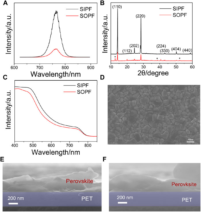
FIGURE 1. Characterization of the constructed perovskite thin film based on the solvent-induced method. (A) time-resolved PL, (B) XRD, and (C) absorption spectrum. (D) top-view SEM image of the SIPF (E) and (F) cross-section SEM images for the SOPF and SIPF films.
Current–voltage (I-V) curves of the flexible PD are analyzed by a digital source meter Keithley 2,400 in the atmosphere at room temperature. A set of light-emitting diodes with different wavelengths are used for the incident light source. As shown in Figure 2A, the SIPF-based device dark current (Idark) and photocurrents under illumination light changing from 405 to 880 nm are exhibited. The Idark, obtained from the data, is 4 × 10⁻⁷ A at 1 V bias. When the PD is illuminated, the photocurrents (Iph) are defined as the current difference between illumination and dark which increased dramatically and peaked under the wavelength of 630 nm. The highest Iph value is 2 × 10⁻⁵ A, which is two orders higher than the Idark. Figure 2B shows the I-V curves for the SOPF-based PD. Its highest Iph is about half of the SIPF-based device. The photo-to-dark current ratio (Iph/Idark), which is a very important parameter for a PD, becomes doubly higher based on the obtained data. It indicates the high-quality perovskite film–based flexible PD has an enhanced signal-to-noise ratio. The Iph comparison results for the two devices are presented in Figure 2C in detail. To further evaluate the performance of the flexible PDs, the critical parameters, EQE and R, are obtained and discussed in detail below.
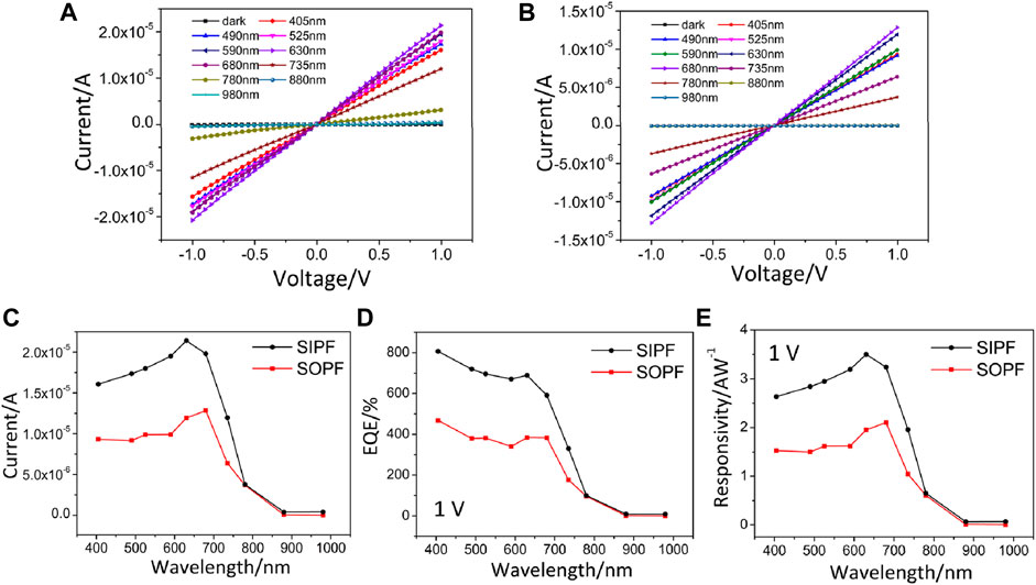
FIGURE 2. Properties of the perovskite MAPbI3 thin-film PD. (A) I–V curves for the SIPF device. (B) I–V curves for the SOPF device. (C) Iph, (D) EQE, and (E) R comparison for the SIPF- and SOPF-based PDs.
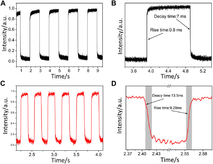
FIGURE 3. Photo-response speed of the flexible device. (A) Multi-cycle for SIPF, (B) Single cycle for SIPF, (C) Multi-cycle for SOPF, (D) Single cycle for SOPF.
Stability is an important factor affecting device suitability for practical applications in portable electronic devices. The long-term stability tests are then performed while being encapsulated by a PMMA film. Figures 4A and B show the device performance changing with the working time. The SIPF-based flexible PD shows a high stable Iph, EQE, and R after working, lasting over 15 days. This suggests that the obtained high-quality perovskite film is characterized by excellent long-term stability.
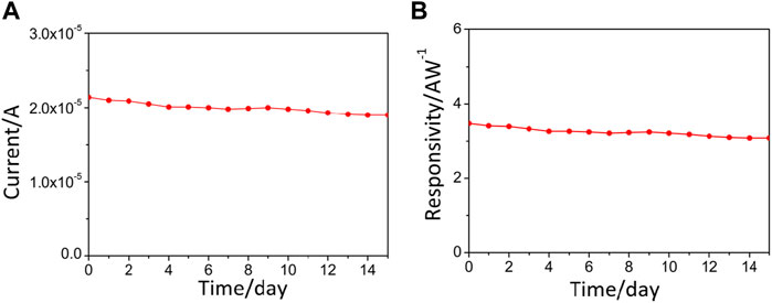
FIGURE 4. Long-term stability of the SIPF-based PD. (A) photocurrent and (B) responsivity changing with time.
3 Conclusion
In summary, a novel solvent-induced fabrication method has been used to synthesize perovskite thin films on flexible substrates. The high-quality MAPbI3 thin film is successfully fabricated and further applied to the flexible PD. Compared with the reported results, this method achieves a low-temperature and low-cost perovskite thin film fabrication process on a flexible substrate. The constructed MAPbI3 layer possesses the advantages of being highly crystalline, uniform, and compact in a large area. The flexible PD based on the as-prepared perovskite thin film exhibits excellent performance and long-term stability. The EQE and R of the flexible PDs reached 8 × 10²% and 3.6 A/W, respectively. At the same time, the flexible PDs still showed superior stability and high performance after 15 days of continuous working. The presented high-quality perovskite thin-film fabrication method and high-performance flexible perovskite PDs are expected to be applied in developing novel opto-electronic devices.
Data Availability Statement
The raw data supporting the conclusions of this article will be made available by the authors, without undue reservation.
Author Contributions
ZL and SS performed the experiments and measurements. PH supervised this work. TZ and SL reviewed and edited this manuscript.
Funding
The authors are grateful to the National Natural Science Foundation of China (51874234, 52104215, 52104216, 51774234, and 51734007).
Conflict of Interest
The authors declare that the research was conducted in the absence of any commercial or financial relationships that could be construed as a potential conflict of interest.
Publisher’s Note
All claims expressed in this article are solely those of the authors and do not necessarily represent those of their affiliated organizations, or those of the publisher, the editors, and the reviewers. Any product that may be evaluated in this article, or claim that may be made by its manufacturer, is not guaranteed or endorsed by the publisher.
References
Alwadai, N., Haque, M. A., Mitra, S., Flemban, T., Pak, Y., Wu, T., et al. (2017). High-Performance Ultraviolet-To-Infrared Broadband Perovskite Photodetectors Achieved via Inter-/Intraband Transitions. ACS Appl. Mat. Interfaces 9, 37832–37838. doi:10.1021/acsami.7b09705
Bai, F., Qi, J., Li, F., Fang, Y., Han, W., Wu, H., et al. (2018). A High-Performance Self-Powered Photodetector Based on Monolayer MoS2/Perovskite Heterostructures. Adv. Mat. Interfaces 5, 1701275. doi:10.1002/admi.201701275
Caldeira Filho, A. M., and Mulato, M. (2011). Characterization of Thermally Evaporated Lead Iodide Films Aimed for the Detection of X-Rays. Nucl. Instrum. Methods Phys. Res. Sect. A Accel. Spectrom. Detect. Assoc. Equip. 636, 82–86. doi:10.1016/j.nima.2011.01.093
Dong, R., Fang, Y., Chae, J., Dai, J., Xiao, Z., Dong, Q., et al. (2015). High-Gain and Low-Driving-Voltage Photodetectors Based on Organolead Triiodide Perovskites. Adv. Mat. 27, 1912–1918. doi:10.1002/adma.201405116
Dou, L., Yang, Y., You, J., Hong, Z., Chang, W.-H., Li, G., et al. (2014). Solution-processed Hybrid Perovskite Photodetectors with High Detectivity. Nat. Commun. 5, 5404. doi:10.1038/ncomms6404
Hu, W., Cong, H., Huang, W., Huang, Y., Chen, L., Pan, A., et al. (2019). Germanium/Perovskite Heterostructure for High-Performance and Broadband Photodetector from Visible to Infrared Telecommunication Band. Light Sci. Appl. 8, 106. doi:10.1038/s41377-019-0218-y
Hu, W., Huang, W., Yang, S., Wang, X., Jiang, Z., Zhu, X., et al. (2017). High-Performance Flexible Photodetectors Based on High-Quality Perovskite Thin Films by a Vapor-Solution Method. Adv. Mat. 29, 1703256. doi:10.1002/adma.201703256
Kang, D. H. (2016). An Ultrahigh-Performance Photodetector Based on a Perovskite–Transition-Metal-Dichalcogenide Hybrid Structure. Adv. Mat. 28, 7799. doi:10.1002/adma.201600992
Kojima, A., Teshima, K., Shirai, Y., and Miyasaka, T. (2009). Organometal Halide Perovskites as Visible-Light Sensitizers for Photovoltaic Cells. J. Am. Chem. Soc. 131, 6050–6051. doi:10.1021/ja809598r
Lee, M. M., Teuscher, J., Miyasaka, T., Murakami, T. N., and Snaith, H. J. (2012). Efficient Hybrid Solar Cells Based on Meso-Superstructured Organometal Halide Perovskites. Science 338, 643–647. doi:10.1126/science.1228604
Li, N., Tao, S., Chen, Y., Niu, X., Onwudinanti, C. K., Hu, C., et al. (2019). Cation and Anion Immobilization through Chemical Bonding Enhancement with Fluorides for Stable Halide Perovskite Solar Cells. Nat. Energy 4, 408–415. doi:10.1038/s41560-019-0382-6
Lian, Z. (2015). High-Performance Planar-Type Photodetector on (100) Facet of MAPbI3 Single Crystal. Sci. Rep. 5, 16563. doi:10.1038/srep07723
Lin, Y. H., Pattanasattayavong, P., and Anthopoulos, T. D. (2017). Metal‐Halide Perovskite Transistors for Printed Electronics: Challenges and Opportunities. Adv. Mat. 29, 1702838. doi:10.1002/adma.201702838
Manser, J. S., Saidaminov, M. I., Christians, J. A., Bakr, O. M., and Kamat, P. V. (2016). Making and Breaking of Lead Halide Perovskites. Acc. Chem. Res. 49, 330–338. doi:10.1021/acs.accounts.5b00455
Mei, J., Liu, M., Vivo, P., and Pecunia, V. (2021). Two‐Dimensional Antimony‐Based Perovskite‐Inspired Materials for High‐Performance Self‐Powered Photodetectors. Adv. Funct. Mat. 31, 2106295. doi:10.1002/adfm.202106295
Mujahid, M., Chen, C., Hu, W., Wang, Z.-K., and Duan, Y. (2020). Progress of High‐Throughput and Low‐Cost Flexible Perovskite Solar Cells. Sol. RRL 4, 1900556. doi:10.1002/solr.201900556
Park, S., Wang, G., Cho, B., Kim, Y., Song, S., Ji, Y., et al. (2012). Flexible Molecular-Scale Electronic Devices. Nat. Nanotech 7, 438–442. doi:10.1038/nnano.2012.81
Saidaminov, M. I., Haque, M. A., Savoie, M., Abdelhady, A. L., Cho, N., Dursun, I., et al. (2016). Perovskite Photodetectors Operating in Both Narrowband and Broadband Regimes. Adv. Mat. 28, 8144–8149. doi:10.1002/adma.201601235
Shao, C.-R., and Hu, W. (2020). Lateral Epitaxial Grown of Two-Dimensional Halide Perovskite Heterostructures. Rare Met. 39 (8), 863–864. doi:10.1007/s12598-020-01458-6
Sze, S. M., Coleman, D. J., and Loya, A. (1971). Current Transport in Metal-Semiconductor-Metal (MSM) Structures. Solid-State Electron. 14, 1209–1218. doi:10.1016/0038-1101(71)90109-2
Wang, F., Mei, J., Wang, Y., Zhang, L., Zhao, H., and Zhao, D. (2016). Fast Photoconductive Responses in Organometal Halide Perovskite Photodetectors. ACS Appl. Mat. Interfaces 8, 2840–2846. doi:10.1021/acsami.5b11621
Xia, H.-R., Li, J., Sun, W.-T., and Peng, L.-M. (2014). Organohalide Lead Perovskite Based Photodetectors with Much Enhanced Performance. Chem. Commun. 50, 13695–13697. doi:10.1039/c4cc05960c
Yamada, Y., Nakamura, T., Endo, M., Wakamiya, A., and Kanemitsu, Y. (2014). Photocarrier Recombination Dynamics in Perovskite CH3NH3PbI3 for Solar Cell Applications. J. Am. Chem. Soc. 136, 11610–11613. doi:10.1021/ja506624n
Zheng, Z., Gan, L., Zhang, J., Zhuge, F., and Zhai, T. (2017). An Enhanced UV-Vis-NIR an D Flexible Photodetector Based on Electrospun ZnO Nanowire Array/PbS Quantum Dots Film Heterostructure. Adv. Sci. 4, 1600316. doi:10.1002/advs.201600316
Keywords: flexible photodetector, organometal halide perovskite, solvent-induced crystallization, photodetector, hybrid perovskite
Citation: Lei Z, Shugang L, Tianjun Z, Shuang S and Hongyu P (2022) Solvent-Induced Crystallization Method for High-Performance and Long-Term Stability Flexible Perovskite Photodetectors. Front. Mater. 9:903308. doi: 10.3389/fmats.2022.903308
Received: 24 March 2022; Accepted: 23 May 2022;
Published: 22 July 2022.
Edited by:
Jun Xi, Xi’an Jiaotong University, ChinaReviewed by:
Xiaobao Xu, Nanjing University of Science and Technology, ChinaManing Liu, Tampere University, Finland
Copyright © 2022 Lei, Shugang, Tianjun, Shuang and Hongyu. This is an open-access article distributed under the terms of the Creative Commons Attribution License (CC BY). The use, distribution or reproduction in other forums is permitted, provided the original author(s) and the copyright owner(s) are credited and that the original publication in this journal is cited, in accordance with accepted academic practice. No use, distribution or reproduction is permitted which does not comply with these terms.
*Correspondence: Pan Hongyu, cGFuMDUwMTZAMTI2LmNvbQ==