
94% of researchers rate our articles as excellent or good
Learn more about the work of our research integrity team to safeguard the quality of each article we publish.
Find out more
ORIGINAL RESEARCH article
Front. Mater., 08 June 2022
Sec. Quantum Materials
Volume 9 - 2022 | https://doi.org/10.3389/fmats.2022.887864
This article is part of the Research TopicInnovators in Quantum MaterialsView all 5 articles
Two-dimensional (2D) magnetic materials have recently attracted a great attention due to their potential applications in information processing and storage. It was observed in an experiment that the CrGeTe3/NiO heterostructure shows a higher Curie temperature and a stronger perpendicular anisotropy. This suggests that antiferromagnet NiO can be coupled with ferromagnetic CrGeTe3 by the proximity effect, which enhances ferromagnetism. However, the mechanism behind the coupling is unknown. In this work, we built a CrGeTe3/NiO heterostructure model and investigated the electronic structure and magnetic properties of the CrGeTe3/NiO interface by first-principles calculations. It is shown that the intralayer exchange interaction between the Cr atoms is ferromagnetic, and the interlayer exchange interaction between the Ni atoms and Cr atoms at the interface is antiferromagnetic. The interlayer interaction is equivalent to a magnetic field as strong as
Since the discovery of graphene (Novoselov et al., 2004; Geim and Novoselov, 2007; Geim, 2009), two-dimensional materials, such as hexagonal BN (Kubota et al., 2007) and transition metal dihalides (TMDs), have attracted considerable attention due to their novel properties and potential applications (Mak et al., 2010; Fang et al., 2012). Since a van der Waals heterostructure (Geim and Grigorieva, 2013) was proposed, the types of two-dimensional materials have been greatly enriched. The two-dimensional magnetic materials can be used in new spintronic devices with the advantages of high sensitivity and high storage density (Pesin and MacDonald, 2012; Han et al., 2014; Han, 2016). In the traditional isotropic Heisenberg model, any thermal fluctuation caused by finite temperature will destroy the long-range magnetic order in one- or two-dimensional systems, as stated in the so-called Mermin–Wagner theorem. However, recent studies have shown that magnetic anisotropy can bypass the Mermin–Wagner theorem and result in a long-range ferromagnetic order at finite temperature (Mermin and Wagner, 1966).
Both CrGeTe3 and CrSiTe3 monolayers are 2D ferromagnetic semiconductors, which makes them promising candidates for further applications in spintronics (Žutić et al., 2004; MacDonald et al., 2005; Geim and Grigorieva, 2013; Liu et al., 2016). The intrinsic ferromagnetism of CrGeTe3 and CrSiTe3 monolayers is due to the ferromagnetic superexchange interaction via the 90° Cr-Te-Cr path, which is mediated by the t2g orbital exchange interaction of adjacent high-spin Cr3+ (Casto et al., 2015; Chen et al., 2015; Williams et al., 2015; Liu et al., 2016; Gong et al., 2017). The bulk of CrGeTe3 belongs to the van der Waals crystal, and the layers are bonded together along the c-axis by van der Waals force. This structure makes it easy to peel off a monolayer and combines it with other materials to form a heterostructure. By stacking two-dimensional material layers, the properties of materials can be improved and enhanced. For example, the Curie temperature of the CrI3/MoTe2 heterostructure is higher than that of CrI3 alone (Chen et al., 2019). The Curie temperature of CrX3 can be boosted by the heterostructure of CrX3 and Mene (M = Si, Ge) (Li et al., 2019). Conversely, the band degeneracy at KK′ point of WSe2 can be eliminated by using the neighbor exchange of CrI3 (Zhong et al., 2017).
Recently, an experimental work found that CrGeTe3 on the NiO substrate showed higher Curie temperature and stronger perpendicular magnetic anisotropy (Idzuchi et al., 2019). A CrGeTe3/NiO heterojunction was prepared by depositing NiO on CrGeTe3 flakes. Compared with the free-standing CrGeTe3 flake, the hysteresis loop of the CrGeTe3/NiO heterojunction became a square with a larger coercivity field (Idzuchi et al., 2019). When the thickness of NiO was 50 nm, the Curie temperature of CrGeTe3/NiO heterojunction was as high as 115 K, while the maximum Curie temperature of CrGeTe3 alone is only about 60K. In the experiment, CrGeTe3 with a thickness of 5–200 nm was selected, and the Curie temperature of CrGeTe3/NiO increased. Even if the thickness of the CrGeTe3 flake reached 200 nm, the Curie temperature of CrGeTe3/NiO was higher than that of bulk CrGeTe3. It can be speculated that the antiferromagnet NiO is coupled with CrGeTe3 through the proximity effect, which enhances the ferromagnetism of CrGeTe3. However, the experiment neither gave further analysis nor clarified the micro mechanism of this phenomenon. Therefore, it is necessary to carry out theoretical calculation to explore the microcosmic mechanism behind the experimental phenomena.
In this study, we investigated the electronic structure and magnetism of the CrGeTe3/NiO (111) interface atomistic model by the first-principles calculations and analyzed the interfacial exchange interaction of the CrGeTe3/NiO (111) heterojunction.
The structure and electronic properties of the CrGeTe3/NiO heterojunction are calculated by the density functional theory (DFT) and the projector-augmented wave (PAW) method implemented in the VASP code (Kresse and Furthmüller, 1996a; Kresse and Furthmüller, 1996b; Kresse and Joubert, 1999; Yu et al., 2009). The Perdew–Burke–Ernzerhof (PBE) parameterization of generalized gradient approximation (GGA) (Perdew et al., 1996) is applied as the exchange correlation functional. The on-site Coulomb interaction of 3d electrons in transition metalions strongly impacts the calculated electronic properties. In order to consider the strong localization effect of the d electrons in Cr and Ni atoms, the GGA + U method (Liechtenstein et al., 1995; Dudarev et al., 1998; Han and van Veenendaal, 2012) is applied to tune the spin properties of Cr and Ni atoms. The Hubbard U of Cr and Ni atoms are set to be 3.0 and 5.0 eV, respectively. In order to reduce the interference of the periodic interaction in the perpendicular direction, a vacuum region of 15 Å is added along the c-axis. The atomic positions are completely relaxed until the error of total energy and the residual force within 10–5 eV and 0.05 eV/Å, respectively. The energy cutoff of the plane wave basis is 520 eV. The Brillouin zone integral is performed on a Monkhorst–Pack k-mesh of 2 × 2 × 1 size (Monkhorst and Pack, 1976). Along the high symmetry line Γ (0, 0, 0) → M (1/2, 0, 0) → K (1/3, 1/3, 0) → Γ (0, 0, 0), the band structure is calculated.
According to the experimental results (Idzuchi et al., 2019), the thickness of CrGeTe3 is 5.5–8 nm, while the thickness of NiO is 20–100 nm. Therefore, when building the model, the thickness of the NiO layer should be relatively large, while the thickness of the CrGeTe3 layer is relatively small. In this work, four layers of NiO are used to simulate the substrate. For simplicity, a single layer of CrGeTe3 is put on the NiO layers. In order to make the lattice match better, we selected the NiO (111) plane. In order to have stronger exchange at the interface, we set the Ni layer right at the interface. The optimized lattice constants of NiO (111) and CrGeTe3 (001) surfaces are 5.895 Å and 6.913 Å, respectively. In the CrGeTe3/NiO heterostructure model, CrGeTe3 (001) (
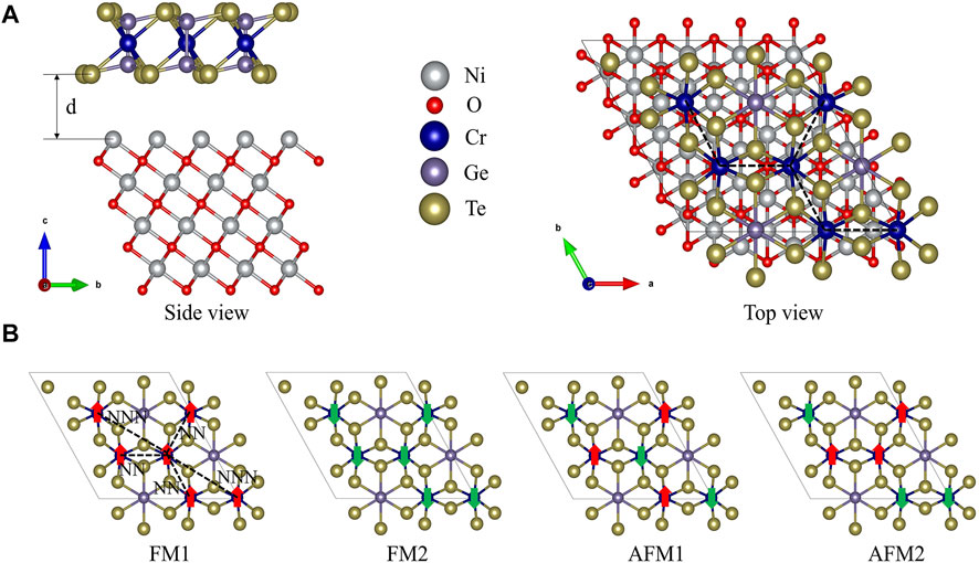
FIGURE 1. (A) Top and side views of the CrGeTe3/NiO heterostructure. (B) Four possible magnetic states of CrGeTe3: FM1, FM2, AFM1, and AFM2.
The total energies of FM1, FM2, AFM1, and AFM2 are −744.05, −744.26, −743.97, and −744.14 eV, respectively. It is obvious that the total energy of FM2 state is the lowest. Its total magnetic moment is −18 μB. Therefore, the ground state of CrGeTe3/NiO heterojunction is the FM2 state, where the exchange interaction in the CrGeTe3 monolayer is ferromagnetic and that between the CrGeTe3 monolayer and the NiO layers is antiferromagnetic. In order to investigate the stability of the FM2 interface system, we further calculated the binding energy, which is defined as
In order to obtain the detailed charge transfer information of the interface, the charge density difference and Bader charge of the CrGeTe3/NiO heterojunction in the FM2 state are calculated. Charge density difference is the redistribution of charge as the CrGeTe3 monolayer is bound to the NiO substrate. In the interface calculation, the bonding of each atom at the interface can be intuitively shown by the charge density difference. The charge density difference can be expressed as
Figure 2A shows the charge density difference of the CrGeTe3/NiO interface in the FM2 state, and Figure 2B zooms in the details of Figure 2A. The cyan area in Figure 2 indicates that the charge density difference is negative, and the yellow region indicates the charge density difference is positive. In Figure 2, the charge transfer results in Ni and Te weak covalent bonds across the interface. In order to further analyze the mechanism of charge transfer, Bader charge analysis is carried out for the system. The results showed that about 1.166 electron is transferred from NiO to CrGeTe3. The charge transfer mainly occurs between the Ni, Te, and Cr atoms near the interface. In the binding process, a Te atom near the interface gets 0.098 electron in average, a Cr atom gets 0.060 electron in average, and the charge change of each Ge atom is negligible. However, the charge redistribution of the atoms away from the interface is negligible as they do not participate in the binding process.
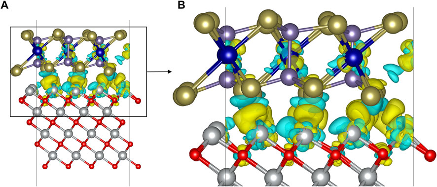
FIGURE 2. Differential charge density (A) and its local enlarged view (B) of the CrGeTe3/NiO interface in the FM2 state. The isosurface is set to 0.021 e/Å3.
In order to study the electronic properties of the CrGeTe3/NiO interface in the FM2 state, the band structure and density of states of the model are calculated. The band structure of the CrGeTe3/NiO heterojunction in the FM2 state is shown in Figure 3. The spin-up and spin-down band gaps are 0.578 and 0 eV, respectively. The total band gap is 0 eV. As a comparison, the band gaps of NiO and CrGeTe3 bulk are calculated to be 2.026 and 0.236 eV, respectively, and those of the NiO (111) surface and CrGeTe3 (001) monolayer are 0.003 and 0.256 eV, respectively. It is obvious that the band gap of the NiO (111) surface is much smaller than that of NiO bulk, and the band gap of the CrGeTe3 (001) monolayer is very close to that of CrGeTe3 bulk. The band gap of the CrGeTe3/NiO heterojunction in the FM2 state is 0 eV, which is smaller than the NiO (111) surface band gap and CrGeTe3 (001) monolayer.
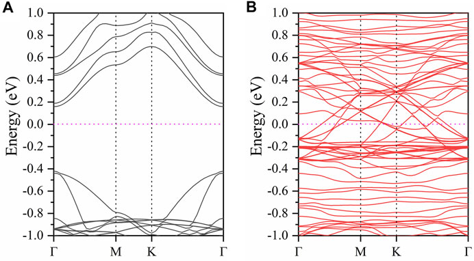
FIGURE 3. Band structure of the CrGeTe3/NiO heterojunction in the FM2 state. (A) and (B) represent the spin-up and spin-down channels, respectively. The Fermi level is set to zero.
The projected density of states of Ni, Te, and Cr atoms near the interface of the CrGeTe3/NiO heterojunction in the FM2 state is shown in Figure 4A. The projected density of states of Te and Cr atoms of the CrGeTe3 alone is shown in Figure 4B. From Figure 4A, it is clear that the state near Fermi level is mainly contributed by the orbitals of Ni, Te, and Cr atoms. Among them, the contribution of the Cr-3d orbital is the largest. The Cr 3d state, the Ni 3d state, and the Te 5p state all pass through the Fermi level. From Figure 4B, it is clear that the state near Fermi level is mainly contributed by the orbitals of Te and Cr atoms. The band gap of CrGeTe3 alone is 0.236 eV, which is significantly larger than that of CrGeTe3/NiO heterojunction.
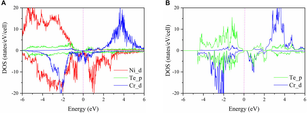
FIGURE 4. (A) Projected density of states (PDOS) for the CrGeTe3/NiO interface in the FM2 state. (B) Projected density of states (PDOS) for CrGeTe3 alone. The Fermi level is set to zero.
By comparing the PDOS in Figures 4A,B, for the spin-up state, it is seen that some new electronic states appear on the CrGeTe3/NiO interface from 0.104 to 0.774 eV nearby the Fermi level. Some electronic states disappear from −0.394 to −0.114 eV nearby the Fermi level. These new electronic states lead to the downward movement of the top of the valence band and the bottom of the conduction band. The final result is that the band gap of the spin-up state of the CrGeTe3/NiO heterojunction becomes smaller. For the spin-down state, it is seen that some new electronic states appear on the CrGeTe3/NiO interface from −0.002 to 0.236 eV nearby the Fermi level. The appearance of these new electronic states leads to the upward movement of the top of the valence band and the downward movement of the bottom of the conduction band. The end result is that the band gap of the spin-down state of the CrGeTe3/NiO heterojunction is reduced to zero.
The occupied Cr-3d orbital cannot appear in both spin-up and spin-down directions. For example, when it is found in the spin-down direction, the spin-up Cr-3d orbital is completely unoccupied. These results can be understood by crystal field theory. Cr3+ ions are located in an octahedral environment coordinated by six Te anions. The Cr-3d orbital splits into three low energy t2g orbitals and two high energy eg orbitals. According to Pauli’s exclusion principle and Hund’s rule, Cr3+ ions will present a high-spin t2g3eg0 electronic configuration, which means that all occupied 3d orbits must be in one spin direction. Among them, the Cr 3d state also contributes to the spin-down state. Also, higher than the Fermi level, the spin-up state is almost occupied by the Cr 3d state, and the spin-down state is almost occupied by the Ni 3d state.
In order to estimate the magnetic couplings in the CrGeTe3/NiO heterojunction, we started from the Heisenberg model:
and it can be rewritten for our specific model:
where
In the CrGeTe3 layer, there are three NN and six NNN Cr atoms for a Cr atom. In FM1 and FM2 structures, there are three NN spin parallel Cr atoms and six NNN spin parallel Cr atoms for a Cr atom. For the interlayer exchange interaction with the NiO substrate, the exchange interaction between a Cr atom and three nearest neighbor Ni atoms is considered. Because the spin directions of Cr and Ni atoms are the same, the interlayer coupling in the FM1 structure is ferromagnetic. Because the spin direction of Cr atom and Ni atom is opposite, the interlayer coupling in the FM2 structure is antiferromagnetic. For an AFM1 structure, there are three NN antiparallel spin Cr atoms and six NNN parallel spin Cr atoms for each Cr atom. In addition, because the sum of the spin of Cr atoms is zero, the summation of the exchange interaction between Cr and Ni atoms is also zero. For the AFM2 structure, the situation is complicated. The interlayer magnetic coupling is the same as AFM1, which is zero. For intralayer magnetic coupling, there are four Cr atoms with one NN parallel spin and two NN antiparallel spin Cr atoms. At the same time, these four Cr atoms also have three NNN parallel spin and three NNN antiparallel spin Cr atoms. The other two Cr atoms have two NN parallel spin and one NN antiparallel spin Cr atoms. At the same time, these two Cr atoms also have six NNN antiparallel spin Cr atoms. Therefore, the total energies of the CrGeTe3/NiO heterojunction in four magnetic states can be written as follows:
where
Substituting the calculated total energies of the four magnetic states into Eq. 4, we can get the following exchange interaction parameters:
Magnets with large magnetic anisotropy energy (MAE) have potential applications in magnetic storage. Magnetic anisotropy can avoid the Mermin–Wagner theorem and make a detour to long-range magnetic order in two-dimensional magnets at a non-zero temperature (Mermin and Wagner, 1966; Torelli et al., 2019). MAE is defined as the energy difference when magnetization is in-plane and out-of-plane, respectively (
The previous experimental result indicates that the CrGeTe3/NiO heterostructure shows a higher Curie temperature than the free-standing CrGeTe3 monolayer (Idzuchi et al., 2019). Therefore, we showed that the Ni–Cr interlayer exchange leads to the increase in Curie temperature of CrGeTe3.
The total exchange energy (Zhong et al., 2017) between the Cr and Ni atoms is
In the Zeeman effect, it is written as follows:
where
Brillouin function is defined by Yosida (1996) as follows:
where
where
where
At thermo equilibrium, the following equation can be obtained as follows:
The left and right sides of Eq. 9 are two functions, respectively, as follows:
At fixed temperature
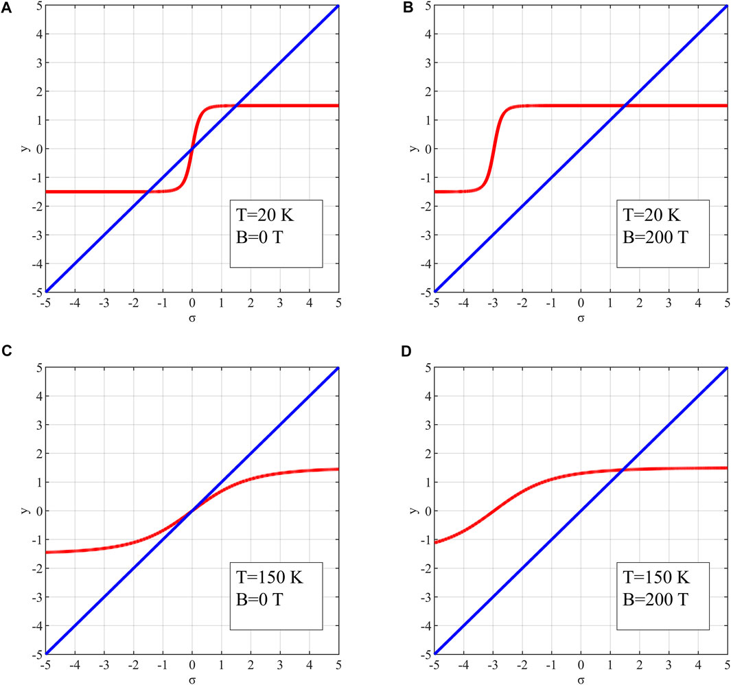
FIGURE 5. Two functions in Eq. 10 with different parameter sets: (A)
In Figures 5A,C, there is no equivalent external field, while there is in Figures 5B,D. In Figure 5A, two functions crossover in the first quadrant, indicating that Eq. 9 has a non-zero solution of
By taking different
It is noticeable that the decrease of
In summary, we built the CrGeTe3/NiO heterojunction model and discovered that the interlayer exchange interaction between the Cr atoms and Ni atoms is antiferromagnetic using the first-principles calculations. We further calculated the electrical and magnetic properties of the CrGeTe3/NiO interface. We inferred that the NiO substrate is equivalent to applying a strong magnetic field of
The raw data supporting the conclusion of this article will be made available by the authors, without undue reservation.
XuL and XZ conceived and implemented the review process. XuL was responsible for the main writing of the manuscript. XZ was responsible for the modification of the manuscript. ZL helped process and check the data part. WZ and HZ helped to build the structure model and provide ideas on magnetic calculation. PY and XiL provided ideas on electronic structure calculation. All authors contributed to the manuscript and approved the submitted version.
This research is supported by the Science Challenge Project (Grant No. TZ2016003-1-105), the Tianjin Natural Science Foundation (Grant No. 20JCZDJC00750), and the Fundamental Research Funds for the Central Universities-Nankai University (Grant No 63211107 and 63201182).
The authors declare that the research was conducted in the absence of any commercial or financial relationships that could be construed as a potential conflict of interest.
All claims expressed in this article are solely those of the authors and do not necessarily represent those of their affiliated organizations, or those of the publisher, the editors, and the reviewers. Any product that may be evaluated in this article, or claim that may be made by its manufacturer, is not guaranteed or endorsed by the publisher.
Casto, L. D., Clune, A. J., Yokosuk, M. O., Musfeldt, J. L., Williams, T. J., Zhuang, H. L., et al. (2015). Strong Spin-Lattice Coupling in CrSiTe3. Apl. Mater. 3, 041515. doi:10.1063/1.4914134
Chen, S., Huang, C., Sun, H., Ding, J., Jena, P., and Kan, E. (2019). Boosting the Curie Temperature of Two-Dimensional Semiconducting CrI3 Monolayer through van der Waals Heterostructures. J. Phys. Chem. C 123, 17987–17993. doi:10.1021/acs.jpcc.9b04631
Chen, X., Qi, J., and Shi, D. (2015). Strain-engineering of Magnetic Coupling in Two-Dimensional Magnetic Semiconductor CrSiTe3: Competition of Direct Exchange Interaction and Superexchange Interaction. Phys. Lett. A 379, 60–63. doi:10.1016/j.physleta.2014.10.042
Dudarev, S. L., Botton, G. A., Savrasov, S. Y., Humphreys, C. J., and Sutton, A. P. (1998). Electron-Energy-Loss Spectra and the Structural Stability of Nickel Oxide: An LSDA+U Study. Phys. Rev. B 57, 1505–1509. doi:10.1103/PhysRevB.57.1505
Fang, H., Chuang, S., Chang, T. C., Takei, K., Takahashi, T., and Javey, A. (2012). High-Performance Single Layered WSe2 P-FETs with Chemically Doped Contacts. Nano Lett. 12, 3788–3792. doi:10.1021/nl301702r
Geim, A. K. (2009). Graphene: Status and Prospects. Science 324, 1530–1534. doi:10.1126/science.1158877
Geim, A. K., and Grigorieva, I. V. (2013). Van der Waals heterostructures. Nature 499, 419–425. doi:10.1038/nature12385
Geim, A. K., and Novoselov, K. S. (2007). The Rise of Graphene. Nat. Mater 6, 183–191. doi:10.1038/nmat1849
Gong, C., Li, L., Li, Z., Ji, H., Stern, A., Xia, Y., et al. (2017). Discovery of intrinsic ferromagnetism in two-dimensional van der Waals crystals. Nature 546, 265–269. doi:10.1038/nature22060
Han, M. J., and van Veenendaal, M. (2012). Spin-moment Formation and Reduced Orbital Polarization in LaNiO3/LaAlO3superlattice:LDA+Ustudy. Phys. Rev. B 85, 195102. doi:10.1103/PhysRevB.85.195102
Han, W., Kawakami, R. K., Gmitra, M., and Fabian, J. (2014). Graphene Spintronics. Nat. Nanotech 9, 794–807. doi:10.1038/nnano.2014.214
Han, W. (2016). Perspectives for Spintronics in 2D Materials. Apl. Mater. 4, 032401. doi:10.1063/1.4941712
Idzuchi, H., Llacsahuanga Allcca, A. E., Pan, X. C., Tanigaki, K., and Chen, Y. P. (2019). Increased Curie Temperature and Enhanced Perpendicular Magneto Anisotropy of Cr2Ge2Te6/NiO Heterostructures. Appl. Phys. Lett. 115, 232403. doi:10.1063/1.5130930
Kresse, G., and Furthmüller, J. (1996). Efficiency of Ab-Initio Total Energy Calculations for Metals and Semiconductors Using a Plane-Wave Basis Set. Comput. Mater. Sci. 6, 15–50. doi:10.1016/0927-0256(96)00008-0
Kresse, G., and Furthmüller, J. (1996). Efficient Iterative Schemes Forab Initiototal-Energy Calculations Using a Plane-Wave Basis Set. Phys. Rev. B 54, 11169–11186. doi:10.1103/PhysRevB.54.11169
Kresse, G., and Joubert, D. (1999). From Ultrasoft Pseudopotentials to the Projector Augmented-Wave Method. Phys. Rev. B 59, 1758–1775. doi:10.1103/PhysRevB.59.1758
Kubota, Y., Watanabe, K., Tsuda, O., and Taniguchi, T. (2007). Deep Ultraviolet Light-Emitting Hexagonal Boron Nitride Synthesized at Atmospheric Pressure. Science 317, 932–934. doi:10.1126/science.1144216
Li, H., Xu, Y.-K., Lai, K., and Zhang, W.-B. (2019). The enhanced ferromagnetism of single-layer CrX3 (X = Br and I) via van der Waals engineering. Phys. Chem. Chem. Phys. 21, 11949–11955. doi:10.1039/C9CP01837A
Liechtenstein, A. I., Anisimov, V. I., and Zaanen, J. (1995). Density-functional Theory and Strong Interactions: Orbital Ordering in Mott-Hubbard Insulators. Phys. Rev. B 52, R5467–R5470. doi:10.1103/PhysRevB.52.R5467
Liu, B., Zou, Y., Zhang, L., Zhou, S., Wang, Z., Wang, W., et al. (2016). Critical Behavior of the Quasi-Two-Dimensional Semiconducting Ferromagnet CrSiTe3. Sci. Rep. 6, 33873. doi:10.1038/srep33873
MacDonald, A. H., Schiffer, P., and Samarth, N. (2005). Ferromagnetic Semiconductors: Moving beyond (Ga,Mn)As. Nat. Mater 4, 195–202. doi:10.1038/nmat1325
Mak, K. F., Lee, C., Hone, J., Shan, J., and Heinz, T. F. (2010). Atomically ThinMoS2: A New Direct-Gap Semiconductor. Phys. Rev. Lett. 105, 136805. doi:10.1103/PhysRevLett.105.136805
Mermin, N. D., and Wagner, H. (1966). Absence of Ferromagnetism or Antiferromagnetism in One- or Two-Dimensional Isotropic Heisenberg Models. Phys. Rev. Lett. 17, 1133–1136. doi:10.1103/physrevlett.17.1133
Monkhorst, H. J., and Pack, J. D. (1976). Special Points for Brillouin-Zone Integrations. Phys. Rev. B 13, 5188–5192. doi:10.1103/physrevb.13.5188
Novoselov, K. S., Geim, A. K., Morozov, S. V., Jiang, D., Zhang, Y., Dubonos, S. V., et al. (2004). Electric Field Effect in Atomically Thin Carbon Films. Science 306, 666–669. doi:10.1126/science.1102896
Perdew, J. P., Burke, K., and Ernzerhof, M. (1996). Generalized Gradient Approximation Made Simple. Phys. Rev. Lett. 77, 3865–3868. doi:10.1103/physrevlett.77.3865
Pesin, D., and MacDonald, A. H. (2012). Spintronics and Pseudospintronics in Graphene and Topological Insulators. Nat. Mater 11, 409–416. doi:10.1038/nmat3305
Torelli, D., Thygesen, K. S., and Olsen, T. (2019). High Throughput Computational Screening for 2D Ferromagnetic Materials: the Critical Role of Anisotropy and Local Correlations. 2D Mat. 6, 045018. doi:10.1088/2053-1583/ab2c43
Williams, T. J., Aczel, A. A., Lumsden, M. D., Nagler, S. E., Stone, M. B., Yan, J.-Q., et al. (2015). Magnetic Correlations in the Quasi-Two-Dimensional Semiconducting ferromagnetCrSiTe3. Phys. Rev. B 92, 144404. doi:10.1103/physrevb.92.144404
Xie, C., Liu, Y., Zhang, Z., Zhou, F., Yang, T., Kuang, M., et al. (2021). Sixfold Degenerate Nodal-point Phonons: Symmetry Analysis and Materials Realization. Phys. Rev. B 104, 045148. doi:10.1103/PhysRevB.104.045148
Yu, J., Lin, X., Wang, J., Chen, J., and Huang, W. (2009). First-principles Study of the Relaxation and Energy of Bcc-Fe, Fcc-Fe and AISI-304 Stainless Steel Surfaces. Appl. Surf. Sci. 255, 9032–9039. doi:10.1016/j.apsusc.2009.06.087
Zhong, D., Seyler, K. L., Linpeng, X., Cheng, R., Sivadas, N., Huang, B., et al. (2017). Van der Waals engineering of ferromagnetic semiconductor heterostructures for spin and valleytronics. Sci. Adv. 3, e1603113. doi:10.1126/sciadv.1603113
Keywords: 2D materials, first-principles calculation, CrGeTe3/NiO interface, exchange interaction, heterostructure
Citation: Liu X, Li Z, Zhang W, Yao P, Zhu H, Liu X and Zuo X (2022) First-Principles Calculations of the Exchange Interaction of the CrGeTe3/NiO Interface. Front. Mater. 9:887864. doi: 10.3389/fmats.2022.887864
Received: 02 March 2022; Accepted: 02 May 2022;
Published: 08 June 2022.
Edited by:
Vincent G. Harris, Northeastern University, United StatesReviewed by:
Xiaotian Wang, Southwest University, ChinaCopyright © 2022 Liu, Li, Zhang, Yao, Zhu, Liu and Zuo. This is an open-access article distributed under the terms of the Creative Commons Attribution License (CC BY). The use, distribution or reproduction in other forums is permitted, provided the original author(s) and the copyright owner(s) are credited and that the original publication in this journal is cited, in accordance with accepted academic practice. No use, distribution or reproduction is permitted which does not comply with these terms.
*Correspondence: Xu Zuo, eHp1b0BuYW5rYWkuZWR1LmNu
Disclaimer: All claims expressed in this article are solely those of the authors and do not necessarily represent those of their affiliated organizations, or those of the publisher, the editors and the reviewers. Any product that may be evaluated in this article or claim that may be made by its manufacturer is not guaranteed or endorsed by the publisher.
Research integrity at Frontiers

Learn more about the work of our research integrity team to safeguard the quality of each article we publish.