
95% of researchers rate our articles as excellent or good
Learn more about the work of our research integrity team to safeguard the quality of each article we publish.
Find out more
ORIGINAL RESEARCH article
Front. Mater. , 28 April 2022
Sec. Quantum Materials
Volume 9 - 2022 | https://doi.org/10.3389/fmats.2022.882008
 A. N. Mihalyuk1,2*
 Y. E. Vekovshinin2L. V. Bondarenko2A. Y. Tupchaya2T. V. Utas2D. V. Gruznev2
 S. V. Eremeev3A. V. Zotov2A. A. Saranin2
Co-adsorption of Pb and Bi onto Si(111) and Ge(111) surfaces has been found to result in formation of atomic-layer PbBi compounds having similar structures. These are two co-existing crystalline PbBi phases with
Reducing crystalline materials from the bulk phase to the two dimensions (2D) creates a rich playground for different exotic electronic phases (Li et al., 2021). Discovery, characterization and control of electronic properties in the 2D materials is a central task of the surface science, where the quantum phenomena emerging in the ultimate two-dimensional case, when the thickness of the film is reduced down to the atomic-scale limit, are of especial interest.
Spin-orbit coupling (SOC) very often plays a key role in many electronic effects observed in the 2D materials. Among other heavy elements, lead and bismuth appear to be the very promising candidates for realizing exotic electronic states, since they have the largest atomic spin-orbit-coupling values and are known to realise unique quantum phenomena in a variety of perspective 1D and 2D materials, such as Pb atomic chains (Mihalyuk et al., 2020) and nanowires (Kopciuszyński et al., 2020) promising for realizing spin-polarized electron transport, plumbene (Zhao et al., 2016; Yuhara et al., 2019) and bismuthene (Luo and Xiang, 2015; Reis et al., 2017) are known to be topological materials, superconducting ultrathin Pb atomic films (Zhang et al., 2010) and ultrathin Bi films (Hirahara et al., 2011) demonstrating 1D topological spin-polarized edge states (Drozdov et al., 2014). There are various bismuth and lead compounds, which are found to be superconductors (Özer et al., 2007) or topological semimetals (Di Bernardo et al., 2021).
The substrate supporting 2D atomic layer plays a crucial role, since it shapes the geometry of the synthesized material and affects its electronic properties. The semiconductor materials became a focus of substantial efforts to the surface engineering, especially silicon- and germanium-based systems (Pillarisetty, 2011). Recently it was found that PbBi compound of atomic thickness grown on silicon surface was found to demonstrate one-dimensional metallic spin-polarized electron states (Mihalyuk et al., 2021) a promising quantum effect relevant for spintronic applications. Remarkably that Pb-Bi films with a nominal thickness of about 4.8 nm grown on silicon demonstrate a superconducting transition at 6.13 K (Tian et al., 2021; Wang et al., 2022). In this regard there is an interest for engineering Pb and Bi containing materials on other semiconducting surfaces.
Among all of the known semiconductor materials, germanium has the highest hole mobility at room temperature (Sammak et al., 2019) (up to 106 cm2 (Vs.)−1), which is about two times larger than the best group III–V p-type semiconductors and silicon. The high hole mobility in the germanium promotes the confinement of spins in the low-disorder Ge quantum dots by uniform potential landscapes (Hendrickx et al., 2018). Another milestone of Ge technology is that virtually every metal on Ge, including superconductors with high critical fields, demonstrate a Fermi level pinned close to the valence band (Dimoulas et al., 2006), which facilitates the injection of holes and, thus, the formation of ohmic superconductor/semiconductor contacts with low Schottky barrier, a key building block in hybrid quantum devices. These advantages make Ge a promising material for quantum technology, as it contains important parameters for semiconducting, superconducting, and topological quantum electronic devices (Scappucci et al., 2021); on the other hand, Ge emerges as an alternative for silicon replacement in future low-power logic applications (Swaminathan et al., 2010), and a key material for boosting the performance of nanodevices (Gomez et al., 2010).
Additional challenge for studying the PbBi layers on Ge(111) is associated with the recent theoretical predictions that Pb3Bi compound with 1.0 ML of Pb and 0.33 ML of Bi possesses a number of fascinating properties, in particular the emergence of van Hove singularity and chiral topological superconducting state (Qin et al., 2019; Li et al., 2020; Sun et al., 2021). These attracting prospects have motivated us to probe the Ge(111) as a platform for synthesizing PbBi compound and studying emergent electronic states. In the present work, we have undertaken combined experimental and theoretical efforts to get insight into the properties of the new material, paying attention to the electronic band structure and impact of the supporting substrate through comparison of the properties of the parent PbBi/Ge(111) and PbBi/Si(111) systems.
Experiments were performed in the ultrahigh-vacuum Omicron MULTIPROBE system (base pressure ≤2.0 × 10⁻¹⁰ Torr) by means of scanning tunneling microscopy (STM) and low-energy electron diffraction (LEED) methods. Ge(111) substrates were cleaned in situ by ion sputtering (0.6 keV for 20 min) followed by direct-current annealing at about 800°C. In order to achieve a well-ordered c (8 × 2) reconstruction, after three such cycles the samples were additionally annealed at 600°C for 3 min. Atomically-clean Si(111)7 ×7 surfaces were prepared in situ by flashing to 1280°C after the samples were first outgassed at 600°C for several hours. Pb and Bi were deposited from the heated tantalum tubes and deposition rates were calibrated using STM observation of corresponding Pb and Bi reconstructions of Ge(111) surface. During the Pb deposition onto the Ge surface the sample temperature was held in the range from 100 to 200°C by indirect heating. In this temperature range, the temperature was measured by a K-type thermocouple installed into the sample stage. STM images were acquired using Omicron variable-temperature STM-XA operating in a constant-current mode. Mechanically cut PtIr tips were used as STM probes after annealing in vacuum.
Density functional theory (DFT) calculations were performed using Vienna Ab initio Simulation Package (VASP) (Kresse and Hafner, 1993; Kresse and Furthmüller, 1996), with core electrons represented by projector augmented wave (PAW) potentials (Blöchl, 1994). The generalized gradient approximation of Perdew, Burke, and Ernzerhof (GGA-PBE) (Perdew et al., 1996) to the exchange-correlation functional was employed for structure relaxation. To simulate the PbBi structure on Ge(111) surface we used a slab consisting of 5 bi-layers (BL) of the substrate with the PBE-optimized bulk Ge lattice constant. Hydrogen atoms were used to passivate the Ge dangling bonds at the bottom of the slab. The atomic positions of PbBi atoms and atoms of Ge layers within the two topmost BLs of the slab were optimized. The geometry optimization was performed until the residual forces on atoms became smaller than 10 meV/Å. The 7 × 7 × 1 and 5 × 5 × 1 k-point mesh was used to sample the (Pb,Bi)/Ge(111)-2 × 2 and (Pb,Bi)/Ge(111)
For more detailed analysis of the interactions of the Pb and Bi atoms with Ge/Si substrates and each other, we performed projected crystal orbital Hamilton population (pCOHP) analysis, (Dronskowski and Bloechl, 1993; Deringer et al., 2011), which is a partitioning scheme of the Kohn–Sham band structure energy in the plane-wave DFT calculations in terms of orbital-pair contributions. For this, we used the Local-Orbital Basis Suite Towards Electronic-Structure Reconstruction (LOBSTER) code (Maintz et al., 2016). The bond-analytical pCOHP provides quantitative information on the bonding, nonbonding, and antibonding contributions in the plane-wave DFT calculations.
In the present STM and LEED experiments, we explored co-adsorption of Pb and Bi onto the Ge(111) and Si(111) surfaces in a wide range of adsorbate coverages, namely in the Ge(111) case we varied the concentration of Bi adsorption onto the β-
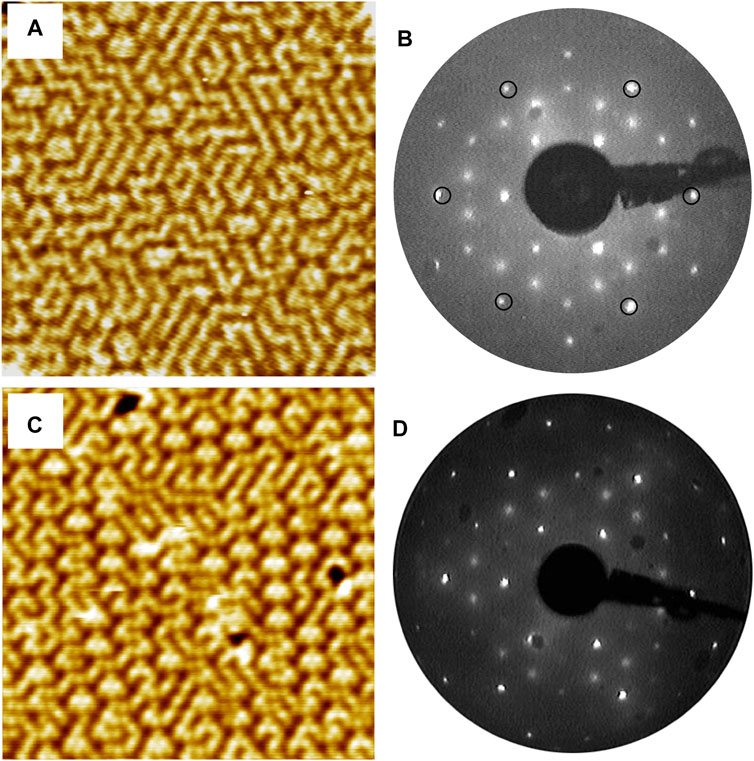
FIGURE 1. Morphology and arrangement of the PbBi atomic layer adsorbed on different substrates. The Ge(111)-based system is characterised by (A) 25 × 29 nm2 (−1.5 V, 0.9 nA) STM image; (B) 79 eV LEED pattern. The Si(111)-based system is characterised by (C) 15 × 15 nm2 (−0.002 V, 200 pA) STM image; (D) 54 eV LEED pattern, recorded at 78 K
Among other varied parameters of Pb and Bi co-adsorption onto the Ge(111) and Si(111) surfaces, there were the growth temperature, typically between room-temperature (RT) and 350°C, and the order of the adsorbed elements, i.e., the PbBi phases can be built either by simultaneous deposition of Pb and Bi elements (followed by annealing) or using successive depositions with intermediate annealing after the deposition of the first adsorbate. General behavior of the PbBi/Ge(111) and PbBi/Si(111) systems was found to be very similar.
Based on experimental data (the surface concentration of each element and periodicity parameters) we conducted the comprehensive ab initio total-energy calculations to find the ground-state atomic models for the both phases, applying AIRSS method. The top views of the obtained lowest-energy models are displayed in Figures 2A,B, where one can see the presence of the distinct rhombus-like motif serving as a building block in both phases. The motif includes pair of Bi atoms and pair of Pb atoms, which all are located in the vicinities of the on-top (T1) sites on the bulk-truncated Ge(111) surface. In the rhombus, Bi dimer forms a short diagonal, while the two separated Pb atoms form a long rhombus diagonal, each being bonded to the bismuth atoms. One can see that in the 2 × 2-PbBi phase motifs are oriented in a single direction (Figure 2A), while in the
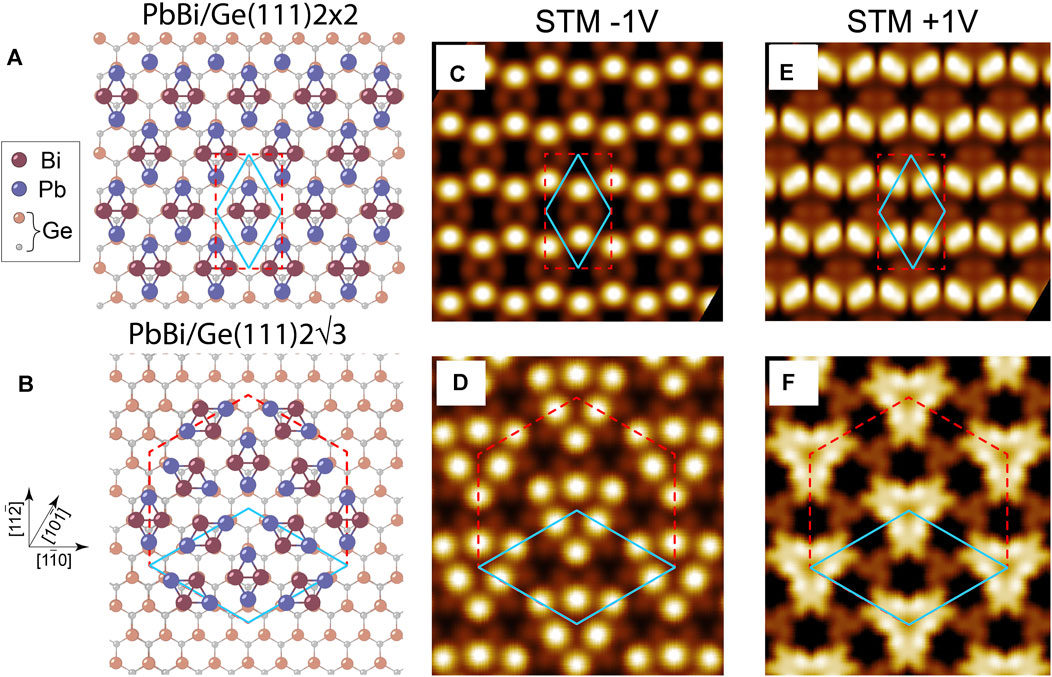
FIGURE 2. Top view atomic models for (A) 2 × 2-PbBi and (B)
Simulated STM images of the 2×2-PbBi phase at the negative bias (or filled states) show the general honeycomb-like appearance (Figure 2C) (as it was also observed in experimental measurements (Figure 1A), although the detailed consideration reveals the 1D nature of STM pattern where bright protrusions are associated with Pb atoms forming a zig-zag charge chain. The positive bias (or empty states) STM simulation produces the very similar one-dimensional appearance of the pattern with bright protrusions associated with Pb-Pb bonds. The STM simulation of the
It is worth noting that established PbBi-Ge(111) ground-state atomic models for two coexisting phases are akin to the recently discovered PbBi-Si(111) phases (Mihalyuk et al., 2021). For this reason, below we give a detailed comparison between the electronic structures of the 2 × 2-PbBi and
Before we start the inspection of electronic properties of the considered systems, let us address the lattice symmetry issue, since it is indispensable for the proper understanding of the emerging electronic effects. The underlying Ge(111) substrate has a C3v symmetry (plane-group p3m), while the rhombus-like motif has a C1h symmetry (plane-group p1), arising from a particular arrangement of the constituent Pb and Bi atoms. So the presence of the PbBi rhombus on the Ge(111) substrate reduces the total symmetry of the system down to C1h for the 2 × 2 case since it contains only one rhombus element bringing the structural anisotropy, but this does not happen in the case of the
Let us start our consideration with the electronic band structure of (Pb,Bi)/Ge(111)-
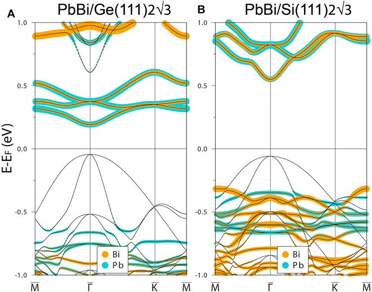
FIGURE 3. The electronic band structure of
One can trace the electronic character of the system from the structural considerations. Note that the geometry itself of the
Interesting that the
Now let us move to the (Pb,Bi)/Ge(111)-2 × 2 phase, which electronic spectrum is presented in Figure 4A along with analogous dispersions calculated for Si(111)-based system (Figure 4B); such a comparison allows us to trace the role of the supporting substrate on the resultant electronic properties. From the element-projected non-relativistic spectrum shown in Figure 4A one can see the highly dispersing S1 metallic surface band propagating within the germanium bulk gap and mainly filled by Pb states denoted in spectrum by blue colored circles. Intersection of the Fermi level gives rise to electron pocket around the
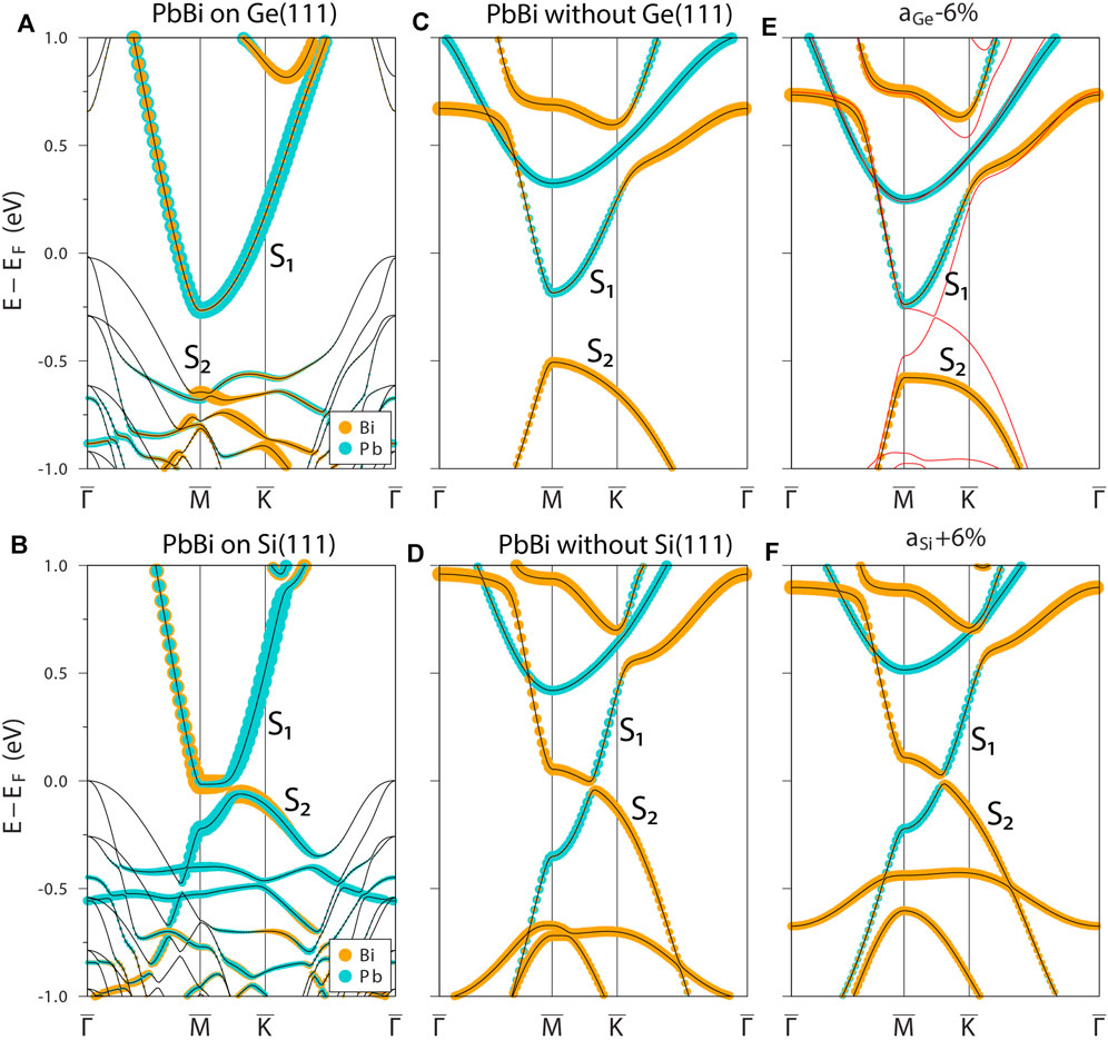
FIGURE 4. Electronic band structure of 2 × 2-PbBi phase supported by germanium (A) and silicon (B) substrates. Panels (C,D) show the spectra for free-standing PbBi layer with germanium and silicon lattice constants, respectfully. Panels (E,F) display the impact of compressive/tensile strain on electronic structure of pristine free-standing PbBi layer. All spectra are calculated in elements-projected non-relativistic form along high-symmetry directions of the 2 × 2 SBZ shown in the inset at the panel (C). The elemental characters of the bands are shown by colored circles.
The last point that remains to be explored is the geometry of the rhombus itself, which is apparently expected to determine the principal features of the electronic spectrum. Figure 5 give the comprehensive comparison between silicon- and germanium-based models of the 2 × 2 phase. It is worth to note that PbBi rhombi on both substrates are not equilateral and have the buckling geometry, i.e., the heights of Pb1 and Pb2 atoms with respect to the position of Bi atoms are slightly different due to the different relief of the underlying substrates. In spite of ≈6% difference between Ge(111) and Si(111) surface unit cell parameters one may see that rhombus parameters such as Bi-Bi, Pb-Bi bondlengths and inside obtuse angle denoted as α are changed insignificantly, while Pb-Pb bondlength and angle of the zig-zag Pb chain denoted as β are changed crucially and, thus, deserve special consideration.
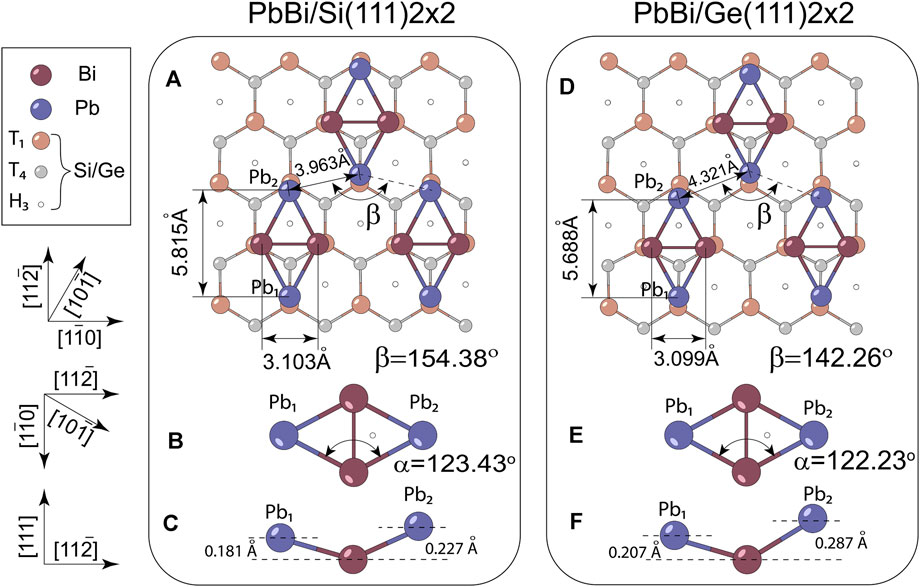
FIGURE 5. The details of 2 × 2-Pb,Bi atomic structure adsorbed on (A–C) Si(111), and (D,E,F) Ge(111) substrates in top and the side views with indication of bond lengths, heights and angles of the rhombi itself (α) and zig-zag Pb chain (β).
In order to scrutinize the bond strengths within rhombi and between rhombi and Ge (Si) substrates, we conducted a chemical-bonding analysis using Crystal Orbital Hamilton Populations method, which results are summarised in Table 1. One can see that among various bonds in the system the strongest are those between Pb (Bi) atoms and nearest substrate atoms, wherein the strength of Pb-Si and Bi-Si interactions is a bit larger than Pb-Ge and Bi-Ge interactions, which is consistent with the shorter bond lengths in the Si case, and longer in the Ge case. However, as we showed above in Figure 4, the interaction of the PbBi atomic layer with underlying substrate does not qualitatively affect the dispersion of the PbBi bands near the Fermi level. Within the distorted rhombus, the Bi-Bi bond is a bit weaker in the Ge-supported structure, whereas the bonds between Bi atoms and two differently located Pb atoms are stronger in this structure in comparison with the Si case. The weakest bond in the PbBi atomic layer is the Pb-Pb one and its length defines the proximity of neighboring rhombi or density of motifs packing. Remarkably, among all other bonds that one has almost the double difference in energy values between Ge and Si cases (see Table 1).
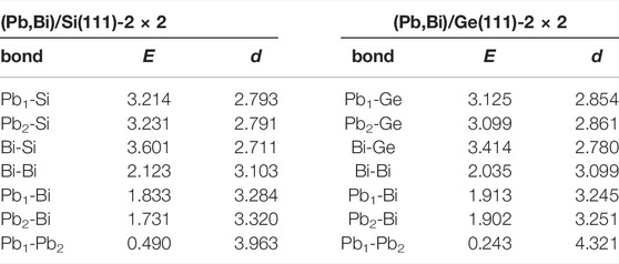
TABLE 1. Bond energies, E (eV), as obtained from integrated pCOHP and corresponding bond lengths, d (Å), between neighboring atoms in the 2 × 2 phases on Si(111) and Ge(111).
With motivation to estimate the impact of Pb-Pb interaction on principal characteristics of electronic spectrum of free-standing PbBi layer we applied a 6% compressive strain to the lattice vectors of Ge-derived unit cell but keeping all parameters of PbBi rhombus unchanged (unlike to the previous strain test, where the uniform changing of all rhombus parameters also took the place). In the result the Pb-Pb distances and angle in the Pb-Pb “zig-zag chain” became almost the same (dPb-Pb = 3.993 Å and β = 150.73°) as in the Si-derived cell. This structural transformation dramatically changed the electronic spectrum (see the red dispersion curves in Figure 4E) shaping it to the character very similar to the Si-derived case (Figure 4D). However, under the uniform 6% compression the Pb-Pb bond length is almost the same, dPb-Pb = 4.084 Å like in the former structure, while the β angle is equal to that the undeformed structure, 142.26°. Thus, one can conclude that change in the β angle of the Pb-Pb zig-zag chain is a key factor responsible for a significant decrease in hybridization between the rhombi (decrease in the Pb-Pb bond strength) and, as a result, an increase in hybridization within PbBi rhombi leading to the modification of the electronic band structure near the Fermi level.
Let us finally examine the impact of spin-orbit coupling effect on the electronic properties of
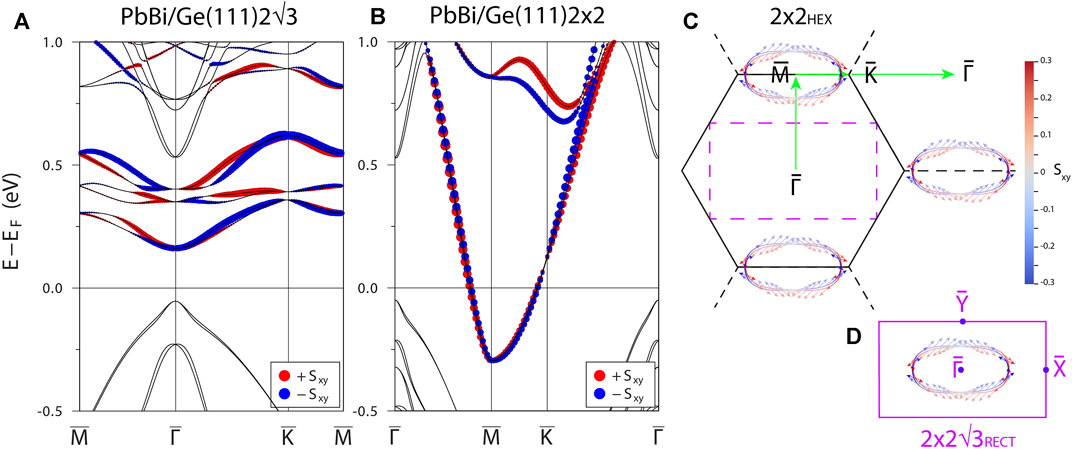
FIGURE 6. Spin-projected relativistic spectra calculated for (A)
We have successfully grown and investigated the structural and electronic characteristics of PbBi atomic layers on Ge(111) and Si(111) surfaces. According to the STM and LEED observations, simultaneous formation of the two crystalline phases with the
The raw data supporting the conclusion of this article will be made available by the authors, without undue reservation.
AM and SE wrote the manuscript and performed the theoretical calculation and analysis, AM and TU produced the figures, LB did the fabrication of materials, AT performed the material characterization, TU analyzed the data, YV performed STM measurements under the guidance of DG, SE contributed to the developing of main concept of the study, AZ contributed to the review and editing of the paper, AS supervised the work and contributed with constructive discussions. All authors discussed the results and implications and commented extensively on the manuscript at all stages.
The experimental work and calculations of germanium-based systems were supported by the RSF Grant No. 21-72-00127. The calculations of silicon-based systems were supported by the Government research assignment for ISPMS SB RAS, project FWRW-2022-0001. The calculations were conducted using the equipment of Shared Resource Center “Far Eastern Computing Resource” IACP FEB RAS (https://cc.dvo.ru).
The authors declare that the research was conducted in the absence of any commercial or financial relationships that could be construed as a potential conflict of interest.
All claims expressed in this article are solely those of the authors and do not necessarily represent those of their affiliated organizations, or those of the publisher, the editors and the reviewers. Any product that may be evaluated in this article, or claim that may be made by its manufacturer, is not guaranteed or endorsed by the publisher.
The Supplementary Material for this article can be found online at: https://www.frontiersin.org/articles/10.3389/fmats.2022.882008/full#supplementary-material
Anisimov, V. I., Zaanen, J., and Andersen, O. K. (1991). Band Theory and Mott Insulators: Hubbard U Instead of Stoner I. Phys. Rev. B 44, 943–954. doi:10.1103/physrevb.44.943
Blöchl, P. E. (1994). Projector Augmented-Wave Method. Phys. Rev. B 50, 17953–17979. doi:10.1103/physrevb.50.17953
Deringer, V. L., Tchougréeff, A. L., and Dronskowski, R. (2011). Crystal Orbital Hamilton Population (COHP) Analysis as Projected from Plane-Wave Basis Sets. J. Phys. Chem. A 115, 5461–5466. doi:10.1021/jp202489s
Di Bernardo, I., Hellerstedt, J., Liu, C., Akhgar, G., Wu, W., Yang, S. A., et al. (2021). Progress in Epitaxial Thin-Film Na3Bi as a Topological Electronic Material. Adv. Mat. 33, 2005897. doi:10.1002/adma.202005897
Dimoulas, A., Tsipas, P., Sotiropoulos, A., and Evangelou, E. K. (2006). Fermi-level Pinning and Charge Neutrality Level in Germanium. Appl. Phys. Lett. 89, 252110. doi:10.1063/1.2410241
Dronskowski, R., and Bloechl, P. E. (1993). Crystal Orbital Hamilton Populations (COHP): Energy-Resolved Visualization of Chemical Bonding in Solids Based on Density-Functional Calculations. J. Phys. Chem. 97, 8617–8624. doi:10.1021/j100135a014
Drozdov, I. K., Alexandradinata, A., Jeon, S., Nadj-Perge, S., Ji, H., Cava, R. J., et al. (2014). One-dimensional Topological Edge States of Bismuth Bilayers. Nat. Phys. 10, 664–669. doi:10.1038/nphys3048
Dudarev, S. L., Botton, G. A., Savrasov, S. Y., Humphreys, C. J., and Sutton, A. P. (1998). Electron-energy-loss Spectra and the Structural Stability of Nickel Oxide: An LSDA+U Study. Phys. Rev. B 57, 1505–1509. doi:10.1103/physrevb.57.1505
Gomez, L., Ni Chlairigh, C., Hashemi, P., and Hoyt, J. L. (2010). Enhanced Hole Mobility in High Ge Content Asymmetrically Strained-SiGe P-MOSFETs. IEEE Electron Device Lett. 31, 782–784. doi:10.1109/led.2010.2050574
Hendrickx, N. W., Franke, D. P., Sammak, A., Kouwenhoven, M., Sabbagh, D., Yeoh, L., et al. (2018). Gate-controlled Quantum Dots and Superconductivity in Planar Germanium. Nat. Commun. 9, 2835. doi:10.1038/s41467-018-05299-x
Hirahara, T., Bihlmayer, G., Sakamoto, Y., Yamada, M., Miyazaki, H., Kimura, S.-i., et al. (2011). Interfacing 2D and 3D Topological Insulators: Bi(111) Bilayer on Bi2Te3. Phys. Rev. Lett. 107, 166801. doi:10.1103/PhysRevLett.107.166801
Kopciuszyński, M., Stepniak-Dybala, A., Dachniewicz, M., Żurawek, L., Krawiec, M., and Zdyb, R. (2020). Hut-shaped Lead Nanowires with One-Dimensional Electronic Properties. Phys. Rev. B 102, 125415. doi:10.1103/PhysRevB.102.125415
Kresse, G., and Furthmüller, J. (1996). Efficient Iterative Schemes Forab Initiototal-Energy Calculations Using a Plane-Wave Basis Set. Phys. Rev. B 54, 11169–11186. doi:10.1103/physrevb.54.11169
Kresse, G., and Hafner, J. (1993). Ab Initiomolecular Dynamics for Liquid Metals. Phys. Rev. B 47, 558–561. doi:10.1103/physrevb.47.558
Li, L., Ren, S., Qin, W., Zhang, S., Wan, X., Jia, Y., et al. (2020). Emergence of Van Hove Singularity and Topological States in Pb3Bi/Ge(111) Rashba Systems. Phys. Rev. B 102, 035150. doi:10.1103/PhysRevB.102.035150
Li, W., Qian, X., and Li, J. (2021). Phase Transitions in 2D Materials. Nat. Rev. Mater 6, 829–846. doi:10.1038/s41578-021-00304-0
Luo, W., and Xiang, H. (2015). Room Temperature Quantum Spin Hall Insulators with a Buckled Square Lattice. Nano Lett. 15, 3230–3235. doi:10.1021/acs.nanolett.5b00418
Maintz, S., Deringer, V. L., Tchougréeff, A. L., and Dronskowski, R. (2016). LOBSTER: A Tool to Extract Chemical Bonding from Plane-Wave Based DFT. J. Comput. Chem. 37, 1030–1035. doi:10.1002/jcc.24300
Mihalyuk, A. N., Bondarenko, L. V., Tupchaya, A. Y., Utas, T. V., Vekovshinin, Y. E., Gruznev, D. V., et al. (2021). One-dimensional Spin-Polarized Electron Channel in the Two-Dimensional PbBi Compound on Silicon. Phys. Rev. B 104, 125413. doi:10.1103/PhysRevB.104.125413
Mihalyuk, A. N., Chou, J. P., Eremeev, S. V., Zotov, A. V., and Saranin, A. A. (2020). One-dimensional Rashba States in Pb Atomic Chains on a Semiconductor Surface. Phys. Rev. B 102, 035442. doi:10.1103/PhysRevB.102.035442
Özer, M. M., Jia, Y., Zhang, Z., Thompson, J. R., and Weitering, H. H. (2007). Tuning the Quantum Stability and Superconductivity of Ultrathin Metal Alloys. Science 316, 1594–1597. doi:10.1126/science.1142159
Perdew, J. P., Burke, K., and Ernzerhof, M. (1996). Generalized Gradient Approximation Made Simple. Phys. Rev. Lett. 77, 3865–3868. doi:10.1103/PhysRevLett.77.3865
Pickard, C. J., and Needs, R. J. (2011). Ab Initiorandom Structure Searching. J. Phys. Condens. Matter 23, 053201. doi:10.1088/0953-8984/23/5/053201
Pillarisetty, R. (2011). Academic and Industry Research Progress in Germanium Nanodevices. Nature 479, 324–328. doi:10.1038/nature10678
Qin, W., Li, L., and Zhang, Z. (2019). Chiral Topological Superconductivity Arising from the Interplay of Geometric Phase and Electron Correlation. Nat. Phys. 15, 796–802. doi:10.1038/s41567-019-0517-5
Reis, F., Li, G., Dudy, L., Bauernfeind, M., Glass, S., Hanke, W., et al. (2017). Bismuthene on a SiC Substrate: A Candidate for a High-Temperature Quantum Spin Hall Material. Science 357, 287–290. doi:10.1126/science.aai8142
Sammak, A., Sabbagh, D., Hendrickx, N. W., Lodari, M., Paquelet Wuetz, B., Tosato, A., et al. (2019). Shallow and Undoped Germanium Quantum Wells: A Playground for Spin and Hybrid Quantum Technology. Adv. Funct. Mat. 29, 1807613. doi:10.1002/adfm.201807613
Scappucci, G., Kloeffel, C., Zwanenburg, F. A., Loss, D., Myronov, M., Zhang, J.-J., et al. (2021). The Germanium Quantum Information Route. Nat. Rev. Mater 6, 926–943. doi:10.1038/s41578-020-00262-z
Sun, S., Qin, W., Li, L., and Zhang, Z. (2021). Chiral Topological Superconducting State with Chern Number C = −2 in pb3Bi/Ge(111). Phys. Rev. B 103, 235149. doi:10.1103/PhysRevB.103.235149
Swaminathan, S., Shandalov, M., Oshima, Y., and McIntyre, P. C. (2010). Bilayer Metal Oxide Gate Insulators for Scaled Ge-Channel Metal-Oxide-Semiconductor Devices. Appl. Phys. Lett. 96, 082904. doi:10.1063/1.3313946
Tian, M.-Y., Wang, J.-F., Du, H.-J., Ma, C.-X., and Wang, B. (2021). Characterization of Structure and Superconducting Properties of Low-Temperature Phase of Pb-Bi Alloy Films. Acta Phys. Sin. 70, 170703. doi:10.7498/aps.70.20210482
Wang, J. F., Tian, M. Y., Du, H. J., Ma, C. X., and Wang, B. (2022). Structural and Superconducting Properties of Ultrathin Pbbi3 Films Fabricated at Low Temperature. Acta Phys. Sin. doi:10.7498/aps.71.20220050
Yuhara, J., He, B., Matsunami, N., Nakatake, M., and Le Lay, G. (2019). Graphene's Latest Cousin: Plumbene Epitaxial Growth on a "Nano WaterCube". Adv. Mat. 31, 1901017. doi:10.1002/adma.201901017
Zhang, T., Cheng, P., Li, W.-J., Sun, Y.-J., Wang, G., Zhu, X.-G., et al. (2010). Superconductivity in One-Atomic-Layer Metal Films Grown on Si(111). Nat. Phys. 6, 104–108. doi:10.1038/nphys1499
Keywords: 2D materials, germanium, silicon, bismuth, lead
Citation: Mihalyuk AN, Vekovshinin YE, Bondarenko LV, Tupchaya AY, Utas TV, Gruznev DV, Eremeev SV, Zotov AV and Saranin AA (2022) Insights Into the Electronic Properties of PbBi Atomic Layers on Ge(111) and Si(111) Surfaces. Front. Mater. 9:882008. doi: 10.3389/fmats.2022.882008
Received: 23 February 2022; Accepted: 13 April 2022;
Published: 28 April 2022.
Edited by:
Ryan Requist, Hebrew University of Jerusalem, IsraelReviewed by:
Xiaotian Wang, Southwest University, ChinaCopyright © 2022 Mihalyuk, Vekovshinin, Bondarenko, Tupchaya, Utas, Gruznev, Eremeev, Zotov and Saranin. This is an open-access article distributed under the terms of the Creative Commons Attribution License (CC BY). The use, distribution or reproduction in other forums is permitted, provided the original author(s) and the copyright owner(s) are credited and that the original publication in this journal is cited, in accordance with accepted academic practice. No use, distribution or reproduction is permitted which does not comply with these terms.
*Correspondence: A. N. Mihalyuk, bWloLWFsZXhleUB5YW5kZXgucnU=
Disclaimer: All claims expressed in this article are solely those of the authors and do not necessarily represent those of their affiliated organizations, or those of the publisher, the editors and the reviewers. Any product that may be evaluated in this article or claim that may be made by its manufacturer is not guaranteed or endorsed by the publisher.
Research integrity at Frontiers
Learn more about the work of our research integrity team to safeguard the quality of each article we publish.