
94% of researchers rate our articles as excellent or good
Learn more about the work of our research integrity team to safeguard the quality of each article we publish.
Find out more
ORIGINAL RESEARCH article
Front. Mater., 22 March 2022
Sec. Quantum Materials
Volume 9 - 2022 | https://doi.org/10.3389/fmats.2022.866468
This article is part of the Research Topic2022 Retrospective: Quantum MaterialsView all 5 articles
 Yichao Liu1†
 Cangmin Wang1†Wenyu Huang1Shaoting Wang2Huaili Qiu1Weifeng Ge1
 Meixia Chen1Hui Zhang3*Yueliang Gu4Xingmin Zhang4Xiaolong Li4Xingyu Gao4
 Yuanjun Yang1*
As a prototype of a strongly correlated electron system, bulk vanadium dioxide (VO2) exhibits a large and reversible metal–insulator transition (MIT) near 340 K, concomitantly accompanied by a monoclinic–rutile structural phase transformation (SPT). In this study, we systematically investigated the SPT across the MIT in a (010)-VO2/(0001)-Al2O3 epitaxial thin film by simultaneously determining three lattice constants (a, b, and c) and the mismatch angle (Δβ) using high-resolution X-ray diffraction. The lattice constants a, b, and c were approximately 5.723, 4.521, and 5.393 Å, respectively, at room temperature, and the mismatch angle was approximately 122.02°. As the temperature increased, the lattice constants and mismatch angle did not change significantly until the temperature reached the MIT point. Then, a, b, and c suddenly increased to approximately 5.689 Å, 4.538 Å, and 5.411 Å, respectively, and retained this value up to nearly 90°C. However, the mismatch angle first slightly increased and then sharply decreased to 122.00°. Additionally, the lattice constants and mismatch angle were almost reproducible with decreasing temperature, except for hysteresis in the MIT region. These results verify that VO2 undergoes an MIT, simultaneously accompanied by SPT, in thicker films with small strain and weak substrate constraints, analogous to bulk VO2. This was further confirmed by in-situ varying-temperature Raman characterization. These findings provide insights into the SPT and reveal an angular parameter for judging the SPT in VO2 systems.
Since Morin first discovered the metal–insulator transition (MIT) behavior in 1959, vanadium oxide (VO2) has attracted great attention owing to its implications in the fundamental sciences and potential technological applications (Morin, 1959; Mott, 1990; Stefanovich et al., 2000; Lysenko et al., 2006; Park et al., 2007; Nakajima et al., 2008; Kevin Wang et al., 2013; Lee et al., 2017; Shi and Chen, 2018; Wall et al., 2018). Bulk VO2 undergoes a thermally-induced MIT with a critical temperature near 340 K, accompanied by a structural phase transformation (SPT) from a low-temperature insulating phase to a high-temperature metallic phase (Mott, 1990; Lee et al., 2017; Shi and Chen, 2018; Wall et al., 2018). Simultaneously, large and reversible changes in electrical (Stefanovich et al., 2000), optical (Lysenko et al., 2006; Nakajima et al., 2008), magnetic (Park et al., 2007), and thermal (Kevin Wang et al., 2013) properties can be achieved in the vicinity of the MIT. In addition, the MIT behavior of VO2 is easily modulated by external stimuli, such as temperature (Liu et al., 2015), strain (Cao et al., 2009; Hu et al., 2010; Aetukuri et al., 2013; Lee et al., 2015), light (Morrison et al., 2014), and electric fields (Nakano et al., 2012; Jeong et al., 2013; Sharma et al., 2018), enabling broad applications in energy saving (Imada et al., 1998), photoelectric switching (Huang et al., 2010), smart windows (Ning Wang et al., 2013; Zhou et al., 2013), infrared devices (Chen et al., 2004), and information storage media (Driscoll et al., 2009; Pellegrino et al., 2012). However, the mechanism of the MIT in VO2 remains unclear; to date, there are three main perspectives. First, strong electron–electron correlation dominantly drives the Mott transition in the VO2 system (Jeong et al., 2013). Second, the electron–phonon mechanism is structurally driven by the Peierls transition (Baum et al., 2007). The third involves the combined action of electron correlation and structural instability (Yao et al., 2010; Cocker et al., 2012). Regardless of the specific mechanism behind different VO2 systems [for example, strained, relaxed in the film state (Lee et al., 2018), or nanostructured samples (Cao et al., 2009)], the SPT is the key link to uncovering the MIT mechanism in VO2.
Extensive studies have been conducted on the SPT and crystal structure of VO2 films, with recent advances in their preparation and growth (Fan et al., 2012; Yu et al., 2017; Lee et al., 2018; Sharma et al., 2018; Zhang et al., 2020). Fan et al. analyzed the structural domain-matching epitaxy relationship between VO2 and a sapphire substrate (Fan et al., 2012), which may be important for understanding the MIT mechanism. Yu et al. obtained VO2 thin films using an oxygen annealing treatment and achieved an insulating monoclinic phase. Moreover, the oxidation conditions affect the microstructure of VO2 films and further modulate its MIT performance (Yu et al., 2017). Lee et al. demonstrated an isostructural, purely electronically driven MIT in VO2-δ/VO2 bilayers on (001)-TiO2 substrates (Lee et al., 2018). Sharma et al. observed the crucial role of oxygen vacancies in controlling the MIT in epitaxial VO2 thin films on Nb-doped TiO2 substrates (Sharma et al., 2018). Zhang et al. compared the crystal structure and optical properties of VO2 thin films on silicon, quartz, and sapphire substrates, revealing their distinct behaviors (Zhang et al., 2020). Despite the aforementioned research, SPT across the MIT in VO2 thin films is insufficiently understood. To date, in thin-film VO2 systems, the structural unit cell parameters a, b, c and β have not been simultaneously determined to directly reveal SPT behaviors across the MIT.
In this study, we deposited a VO2 thin film on a c-plane sapphire substrate using radio-frequency (RF) magnetron sputtering. The epitaxial relationship between VO2 and the Al2O3 substrate, and temperature-dependent crystal structure evolution were revealed using high-resolution X-ray diffraction (XRD). The lattice constants and mismatch angle of the VO2 film were simultaneously determined to reveal the SPT across the MIT, indicating a distinct phase transition compared to the bulk VO2 system (single crystal or polycrystal).
We deposited VO2 thin films on (0001)-Al2O3 single-crystal substrates with dimensions of 5 × 5 × 0.5 mm using a reactive RF magnetron sputtering technique. A circular vanadium metal target with a purity of 99.99% was sputtered. The RF power was set to 65 W, and the gas pressure was approximately 0.33 Pa. The argon (Ar) and oxygen (O2) flow ratio was set to 50:1.5, and the substrate temperature was set to 520°C. The sputtering distance was approximately 12 cm, and the background pressure was pumped to a value greater than 2.5 × 10⁻⁴ Pa. The film thickness was determined to be approximately 90 nm by controlling the deposition time (Yang et al., 2015a). The orientation, structure, and epitaxial quality of the VO2 thin films were characterized using high-resolution XRD in house with Cu Kα1 and partially on the 14B beamline of the Shanghai Synchrotron Radiation Facility (SSRF) with an X-ray wavelength of ∼1.2395 Å. The HORIBA LabRAM HR Evolution microscope confocal laser Raman spectrometer was used to detect in-situ temperature-varying Raman modes in the VO2 epitaxial films. A laser with a wavelength of 532 nm was selected, and the laser power was set to approximately 0.25 mW. The objective lens was a magnification of ×50, and the unit data acquisition time was 20 s. The rate of temperature change was approximately 10°C/min during the heating process, and the cooling process naturally decreased to room temperature. The temperature was maintained for 4 min after it reached a fixed point to maintain stability and consistency.
Figures 1A,B show the crystal structure of VO2. In general, the SPT in VO2 refers to the process of the monoclinic phase (M1) transforming into the tetragonal phase (R) (Mott, 1990; Shi and Chen, 2018). When the temperature is below the phase transition temperature, VO2 is in a monoclinic phase. In this state, the V atoms in the crystal spontaneously dimerize along the aM-axis, forming a twisted zig-zag chain, as shown in Figure 1A. Because the V–V atoms have two different distances, resulting in the localization of the d-orbital electrons in the V–V dimer, they exhibit the properties of an insulating state (Shimizu et al., 2020). In contrast, in the R phase, as shown in Figure 1B, the V–V atom chain along the cR-axis direction is not paired, leading to the disappearance of V–V dimerization and the emergence of a linear chain (Morrison et al., 2014). As a consequence, the MIT occurs with a resistivity change of nearly three to four orders of magnitude as shown in Figure 1D. Moreover, the resistance vs. temperature curve shows a reversible hysteresis with a critical temperature of approximately 62.9 and 73.6°C in the heating and cooling process (see details in Supplementary Figure S1 in Supplementary Materials).
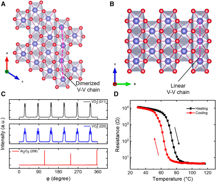
FIGURE 1. Schematic crystal structures of (A) monoclinic VO2 (M1) and (B) rutile VO2 (R), where the blue and red spheres represent vanadium and oxygen atoms, respectively. (C) Full-range X-ray diffraction (XRD) φ-scans of the (011) and (220) planes of the VO2 (M1) thin film relative to the (208) peak of the substrate at room temperature. (D) Resistance (R) of a typical VO2 thin film grown on c-plane Al2O3 substrate as a function of temperature (T).
To verify the growth direction of the VO2 thin film on the (0001) surface of the Al2O3 substrate, we first performed a normal θ-2θ line scan of XRD at room temperature and determined the VO2 [010] along the out-of-plane direction (see the following results), which is consistent with previous reports (Yang et al., 2015a; Muramoto et al., 2020). Second, we confirmed the in-plane growth orientation of the VO2/Al2O3 thin film using high-resolution XRD at room temperature. Figure 1C shows the φ-scan results for the VO2 (011) and (220) and Al2O3 (208) reflections. The positions of the VO2 (011) and (220) peaks were at the same azimuthal position and separated by 60° (Nag et al., 2011). Furthermore, three-fold symmetry of the Al2O3 (208) reflection was also observed owing to the triple symmetry of the (0001) surface with respect to the c-axis of Al2O3 (Zhang et al., 1999; Yang et al., 2011). In addition to a two-fold symmetry with respect to the b-axis in monoclinic VO2, six peaks in both the VO2 (011) and (220) φ-scans were observed, indicating an emergence of the structural twinned domain. Upon close inspection, the individual VO2 (011) peak was found to split into two peaks, that is, a doublet, which was caused by a β-angle mismatch between VO2 and the Al2O3 substrate. Moreover, the individual VO2 (220) peak revealed that each of the main peaks was surrounded by two smaller satellite peaks with a triplet feature, which may be caused by the V–V zig-zag chain deviating from the monoclinic aM-axis (Zhao et al., 2012; Fan et al., 2013; Yang et al., 2018a).
To explore the SPT of VO2 thin films across the MIT, we employed in-situ variable-temperature high-resolution XRD at the BL14B1 beamline of the SSRF. Figures 2A,B show the local θ-2θ scans of epitaxial VO2 films on sapphire substrates during the heating and cooling processes, respectively, in the temperature range 30–90°C. Overall, the Al2O3 (0006) peak barely moved during the entire heating and cooling processes, strongly indicating that thermal effect during heating and cooling process can be ignored in discussing SPT of the VO2 thin films. Whereas the VO2 (020) reflection moved to a lower angle during the heating process and back to a higher angle during the cooling process, indicating a reversible SPT across the MIT. The diffraction peak of VO2 (020) was located at approximately 31.83° at 30°C during the heating and cooling processes. In particular, the 2θ shift of the VO2 (020) reflection was more obvious in the temperature range of approximately 60–70°C, as indicated by the ellipse in Figures 2A,B, then reached approximately 31.72 at 90°C, resulting in elongating of the lattice space of the VO2 (020) plane. Because the b-axis is perpendicular to the VO2 (020) plane, the plane space directly reflects the lattice constant b (Yang et al., 2018b). Consequently, the lattice constant b should be increased upon heating, which is consistent with the occurrence of SPT, as reported in previous studies (Park et al., 2013).
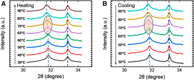
FIGURE 2. Local XRD θ-2θ scan patterns of VO2/Al2O3 during the (A) heating and (B) cooling processes.
By combining the above structural information, we can infer the possible structural domain configuration of the VO2 thin film on the (0001)-Al2O3 substrate, as shown in Figure 3A. The Al2O3 (0001) surface exhibited a hexagonal structure, and the VO2 film was epitaxially grown on it with the b-axis along the out-of-plane direction. Therefore, the a-axis and c-axis of the VO2 film matched the (0001) plane of the Al2O3 substrate. Based on Figures 1C, 2A,B, two types of domain configurations were derived, as shown in Figure 3A. The cM-axis was determined along the Al2O3 [21
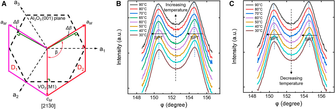
FIGURE 3. (A) Schematic diagram of one typical domain structure pattern of the VO2 (M1) epitaxial thin film on the Al2O3 (0001) interface. Local φ scans of the VO2 (011) reflection under the (B) heating and (C) cooling processes.
Next, we quantitatively determined the other two lattice parameters a and c. The remaining two nonsymmetric reflections, that is, the VO2 (011) and (220) diffraction peaks, were selected. θ-2θ line scans were performed to obtain the temperature-dependent reflection shift using in-house high-resolution XRD with Cu Kα1 radiation. In the XRD line scans of the VO2 (011) reflection, as shown in Figures 4A,B, when the VO2 thin film was in the low-temperature monoclinic phase during the heating process, 2θ was 27.87°; with an increase in temperature, the peak position of 2θ gradually shifted to a lower angle position. Moreover, the change was more obvious in the temperature range 65–70°C; the peak position changed to 27.67° at 90°C. The VO2 (011) reflection shifted back during the cooling process. It is worth mentioning that the monoclinic M2 phase should exist near the interface at relatively lower temperature due to the substrate constraints (Hu et al., 2010). Similarly, in the XRD line scans of the VO2 (220) crystal plane, as shown in Figures 4C,D, the peak position of VO2 (220) shifted to a higher angle position in the heating process and back in the cooling process. Note that, regardless of the heating or cooling process, the peak position of the Al2O3 (116) reflection at 2θ = 57.56° remained unchanged, which is a good indicator for the SPT in VO2 thin films.
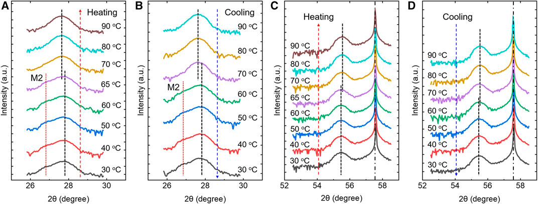
FIGURE 4. XRD line scans of the VO2 (011) reflections under the (A) heating and (B) cooling processes. The M2 phase at lower temperature disappears with the increase of temperature over the MIT temperature. XRD line scans of VO2 (220) reflections under the (C) heating and (D) cooling processes.
Using local θ-2θ scans of the (020) peaks of VO2, the out-of-plane lattice parameter b can be obtained using the Bragg formula:
Where β is the mismatch angle between the a- and c-axis in the VO2 crystal structure. This can be obtained from Figures 3B,C, as mentioned above (Longo et al., 1970). Next, we can simultaneously calculate the lattice parameters a and c during the heating and cooling processes.
The lattice constants a, b, and c, and the β angle during the heating and cooling processes are summarized in Figure 5. Overall, the lattice parameters of the monoclinic VO2 film at a low temperature (∼30°C) were a = 5.723 Å, b = 4.521 Å, c = 5.393 Å, and the included angle β = 122.01°. Comparing with the bulk lattice constants a, b, and c approximately 5.755, 4.525, and 5.383 Å (Rakotoniaina et al., 1993), the out-of-plane strain seems relaxed. Moreover, the tensile strain along the cM-axis indeed establishes, which should be due to the thermal expansion mismatch between the VO2 thin film and Al2O3 subsstrate (Théry et al., 2016). However, the in-plane strain along the aM-axis is compressive, which may be responsible for the volume conservation of VO2 unit cell. Therefore, herein the biaxial anisotropic strain is developed and does not seem to affect the MIT temperature as shown Figure 1D. This case is different from the biaxial tensile strain in Ref. 49. As increasing temperature, the lattice parameters of the high-temperature tetragonal VO2 film were a = 5.689 Å, b = 4.538 Å, c = 5.411 Å, and β = 122.00°. It is mentionable that the determination of the lattice constant in the high-temperature rutile phase is still in the framework of the monoclinic symmetry for better illustrating the lattice change across the MIT, the same as the low-temperature monoclinic phase. Interestingly, the lattice parameter c in the (010)-VO2/(0001)-Al2O3 epitaxial thin films in this study increased during the heating process, whereas the lattice parameters a and c of bulk VO2 both decreased during the transition from the monoclinic to tetragonal phase (Rakotoniaina et al., 1993), Such a distinct change trend could be attributed to the substrate-induced thermal strain in the (010)-VO2/(0001)-Al2O3 epitaxial thin film (Yang et al., 2015a; Théry et al., 2016; Yang et al., 2018a), which will be further studied in the future. Moreover, as indicated in pale blue in Figure 5, sharp changes in the lattice constants a, b, and c, and angle β were observed, indicating the occurrence of the SPT in the heating and cooling processes (Park et al., 2013; McGee et al., 2018). Combined with the transport properties shown in Figure 1D and Supplementary Figure S1, the emergence of SPT is a natural concomitant of the MIT in VO2/Al2O3 thin films (Zhang et al., 2017). In particular, as shown in Figure 5D, a clear increase in the angle β was observed during the heating process, which could be related to the disappearance of the M2 phase in the vicinity of the MIT (Hu et al., 2010; Pellegrino et al., 2012). This conjecture is evidenced in Figures 4A,B.
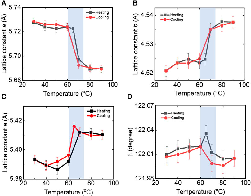
FIGURE 5. For epitaxial VO2 films on c-plane sapphire substrates, the lattice constants a (A), b (B), and c (C), and the included angle β (D) as a function of temperature. The solid square and circle represent the heating process and solid cooling process, respectively. The shaded area represents the structural phase transformation (SPT) region.
To confirm the above SPT, in-situ variable temperature Raman characterization was carried out, as shown in Figures 6A,B. First, overall, the temperature-variable Raman spectra were reversible in the heating and cooling processes. Additionally, there was significant hysteresis in the temperature range of approximately 65–70°C. Second, during the heating process, the characteristic Raman peak at 70°C, shown in Figure 6A, disappeared, indicating SPT from the M1 to R phase. The SPT temperature was close to the MIT temperature. As the temperature continued to increase, the peaks in the Raman spectrum gradually became weaker and eventually disappeared. This corresponds to the first-order phase transition of the crystal structure of VO2 from a low-symmetry monoclinic phase to a high-symmetry rutile phase. Conversely, as shown in Figure 6B, during the cooling process, the peaks in the Raman spectrum gradually recovered and finally agreed with the typical VO2 Raman spectrum of the low-temperature M1 phase. This corresponds to the SPT of VO2 thin films from a high-symmetry rutile phase to a low-symmetry monoclinic phase (Pan et al., 2004). Moreover, we investigated the three characteristic peaks in the Raman spectra of the VO2/Al2O3 epitaxial film in detail, which were located at 194, 226, and 616 cm−1 (Marini et al., 2008; Yu et al., 2013; Chang et al., 2014). These were assigned to the Ag vibrational modes associated with V–V dimerization, which are indicated by stars in Figures 6A,B. The other weaker Ag vibrational modes were located at approximately 145, 311, 390 and 500 cm−1. The peaks reflecting the V–O Bg vibrational mode were located at approximately 263, 342, 447 cm−1 (Ji et al., 2014). These distinct vibrational peaks indicate that the VO2 epitaxial film is essentially insulating with a monoclinic phase (M1). Moreover, the sharp and strong intensity of the Ag mode indicates that the VO2/Al2O3 epitaxial film has a good crystal quality, which is consistent with the above XRD characterization results.
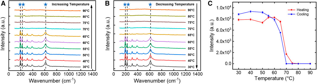
FIGURE 6. Raman spectra of the (A) heating process and (B) cooling process of VO2/Al2O3 epitaxial films. The stars in the figure represent Ag modes in the VO2 film. (C) The relative integrated intensity of the Raman characteristic peak of the Ag mode located at 194 cm−1 as a function of temperature. The error bars are propagated from the calculated integrated intensity.
Following this, we performed Gaussian fitting on the corresponding characteristic peak at 194 cm−1 and obtained the relationship between the relative integral intensity of this peak and the in-situ variable temperature, as shown in Figure 6C. The relative integral intensities of the characteristic peaks in the other two representative Ag modes as a function of temperature are shown in Supplementary Figure S2 of the Supplementary Material. The integral intensity of the characteristic Ag mode exhibited an abrupt change in the temperature region of approximately 65–70°C in both the heating and cooling processes, which verifies that SPT occurs near the MIT in VO2 thin films. Additionally, at high temperatures, the relative integrated intensity of the Ag mode almost decreased to zero, indicating that the monoclinic insulating phase no longer existed. It is mentionable that a slight enhancement of the relative integrated intensity as cycling back to room temperature was probably attributed to a reduction of light absorption, owing to decreasing pressure of the sample chamber. Moreover, at high temperatures, the Raman spectra exhibited almost no characteristic peaks, which is a typical feature of the tetragonal metallic phase (Ji et al., 2014). These results strongly demonstrate that reversible SPT occurs concomitantly across the MIT in (010)-VO2/(0001)-Al2O3 thin films from the perspective of temperature parameter space.
In summary, we successfully grew VO2 epitaxial films on Al2O3 (0001) substrates using reactive magnetron sputtering. The VO2 epitaxial thin films exhibited a clear MIT behavior in the temperature range of approximately 65–70°C. A remarkable feature is the sharp change in the lattice parameters a, b, and c from 5.723, 4.521, and 5.393 Å at low temperatures to 5.689, 4.538, and 5.411 Å, at high temperatures, respectively. Additionally, the included angle β increased from 122.01° at 30°C then sharply decreased at the MIT temperature, implying the occurrence of SPT. By combining quantitative structure characterizations and transport property measurements, the co-occurrence of the SPT and MIT was experimentally observed from the perspective of temperature parameter space in the (010)-VO2/(0001)-Al2O3 thin films, which was further confirmed by Raman spectroscopy. Moreover, the SPT in such thin-film systems is distinct from its bulk counterparts (for example, single-crystal, polycrystalline, or nanostructured samples). This study provides a general strategy for re-examining the SPT in different VO2 systems.
The raw data supporting the conclusions of this article will be made available by the authors, without undue reservation.
YY and HZ conceived this work and designed the experiments. CW and WH optimized the VO2 thin films growth conditions and performed transport property characterizations. YL and SW fabricated the thin films. YL, WG, and MC performed Raman characterization. YG, XZ, XL, XG, and YY carried out XRD characterization. CW performed experimental data analysis and gave a very valuable discussion. YL and YY wrote the paper. All the authors have revised it and gave a last approval to this work.
This research was mainly supported by the Open Foundation of the University of Science and Technology of China (KF2020002) and partially funded by the National Natural Science Foundation of China (52072102, 11804324, and 12074357) and the National Key Research and Development Program of China (2017YFA0205004).
The authors declare that the research was conducted in the absence of any commercial or financial relationships that could be construed as a potential conflict of interest.
All claims expressed in this article are solely those of the authors and do not necessarily represent those of their affiliated organizations, or those of the publisher, the editors and the reviewers. Any product that may be evaluated in this article, or claim that may be made by its manufacturer, is not guaranteed or endorsed by the publisher.
HZ is especially grateful for the support from the Chinese Academy of Sciences Pioneer Hundred Talents Program. The authors highly appreciate the beamlines BL07W, BL10B, BL11U, and BL12B-α at the National Synchrotron Radiation Laboratory (NSRL) for the preliminary characterization of the electronic structure.
The Supplementary Material for this article can be found online at: https://www.frontiersin.org/articles/10.3389/fmats.2022.866468/full#supplementary-material
Aetukuri, N. B., Gray, A. X., Drouard, M., Cossale, M., Gao, L., Reid, A. H., et al. (2013). Control of the Metal-Insulator Transition in Vanadium Dioxide by Modifying Orbital Occupancy. Nat. Phys. 9, 661–666. doi:10.1038/nphys2733
Baum, P., Yang, D.-S., and Zewail, A. H. (2007). 4D Visualization of Transitional Structures in Phase Transformations by Electron Diffraction. Science 318, 788–792. doi:10.1126/science.1147724
Cao, J., Ertekin, E., Srinivasan, V., Fan, W., Huang, S., Zheng, H., et al. (2009). Strain Engineering and One-Dimensional Organization of Metal-Insulator Domains in Single-crystal Vanadium Dioxide Beams. Nat. Nanotech 4, 732–737. doi:10.1038/nnano.2009.266
Chang, S.-J., Park, J. B., Lee, G., Kim, H. J., Lee, J.-B., Bae, T.-S., et al. (2014). In Situ probing of Doping- and Stress-Mediated Phase Transitions in a Single-Crystalline VO2 Nanobeam by Spatially Resolved Raman Spectroscopy. Nanoscale 6, 8068–8074. doi:10.1039/c4nr01118j
Chen, S., Ma, H., Yi, X., Xiong, T., Wang, H., and Ke, C. (2004). Smart VO2 Thin Film for protection of Sensitive Infrared Detectors from strong Laser Radiation. Sensors Actuators A: Phys. 115, 28–31. doi:10.1016/j.sna.2004.03.018
Chen, C., Zhu, Y., Zhao, Y., Lee, J. H., Wang, H., Bernussi, A., et al. (2010). VO2 Multidomain Heteroepitaxial Growth and Terahertz Transmission Modulation. Appl. Phys. Lett. 97, 211905. doi:10.1063/1.3519361
Cocker, T. L., Titova, L. V., Fourmaux, S., Holloway, G., Bandulet, H.-C., Brassard, D., et al. (2012). Phase Diagram of the Ultrafast Photoinduced Insulator-Metal Transition in Vanadium Dioxide. Phys. Rev. B 85, 155120. doi:10.1103/physrevb.85.155120
Driscoll, T., Kim, H.-T., Chae, B.-G., Kim, B.-J., Lee, Y.-W., Jokerst, N. M., et al. (2009). Memory Metamaterials. Science 325, 1518–1521. doi:10.1126/science.1176580
Fan, L. L., Wu, Y. F., Si, C., Zou, C. W., Qi, Z. M., Li, L. B., et al. (2012). Oxygen Pressure Dependent VO2 crystal Film Preparation and the Interfacial Epitaxial Growth Study. Thin Solid Films 520, 6124–6129. doi:10.1016/j.tsf.2012.05.086
Fan, L. L., Wu, Y. F., Si, C., Pan, G. Q., Zou, C. W., and Wu, Z. Y. (2013). Synchrotron Radiation Study of VO2 crystal Film Epitaxial Growth on Sapphire Substrate with Intrinsic Multi-Domains. Appl. Phys. Lett. 102, 011604. doi:10.1063/1.4775580
Hu, B., Ding, Y., Chen, W., Kulkarni, D., Shen, Y., Tsukruk, V. V., et al. (2010). External-Strain Induced Insulating Phase Transition in VO2 Nanobeam and its Application as Flexible Strain Sensor. Adv. Mater. 22, 5134–5139. doi:10.1002/adma.201002868
Huang, W.-x., Yin, X.-g., Huang, C.-p., Wang, Q.-j., Miao, T.-f., and Zhu, Y.-y. (2010). Optical Switching of a Metamaterial by Temperature Controlling. Appl. Phys. Lett. 96, 261908. doi:10.1063/1.3458706
Imada, M., Fujimori, A., and Tokura, Y. (1998). Metal-Insulator Transitions. Rev. Mod. Phys. 70, 1039–1263. doi:10.1103/revmodphys.70.1039
Jeong, J., Aetukuri, N., Graf, T., Schladt, T. D., Samant, M. G., and Parkin, S. S. P. (2013). Suppression of Metal-Insulator Transition in VO2 by Electric Field-Induced Oxygen Vacancy Formation. Science 339, 1402–1405. doi:10.1126/science.1230512
Ji, Y., Zhang, Y., Gao, M., Yuan, Z., Xia, Y., Jin, C., et al. (2014). Role of Microstructures on the M1-M2 Phase Transition in Epitaxial VO2 Thin Films. Sci. Rep. 4, 4854. doi:10.1038/srep04854
Wang, K., Cheng, C., Cardona, E., Guan, J., Liu, K., and Wu, J. (2013). Performance Limits of Microactuation with Vanadium Dioxide as a Solid Engine. ACS Nano 7, 2266–2272. doi:10.1021/nn305419e
Lee, S., Meyer, T. L., Sohn, C., Lee, D., Nichols, J., Lee, D., et al. (2015). Electronic Structure and Insulating gap in Epitaxial VO2 Polymorphs. APL Mater. 3 (12), 126109. doi:10.1063/1.4939004
Lee, S., Hippalgaonkar, K., Yang, F., Hong, J., Ko, C., Suh, J., et al. (2017). Anomalously Low Electronic thermal Conductivity in Metallic Vanadium Dioxide. Science 355, 371–374. doi:10.1126/science.aag0410
Lee, D., Chung, B., Shi, Y., Kim, G.-Y., Campbell, N., Xue, F., et al. (2018). Isostructural Metal-Insulator Transition in VO2. Science 362, 1037–1040. doi:10.1126/science.aam9189
Liu, M., Sternbach, A. J., Wagner, M., Slusar, T. V., Kong, T., Bud'ko, S. L., et al. (2015). Phase Transition in Bulk Single Crystals and Thin Films of VO2 by Nanoscale Infrared Spectroscopy and Imaging. Phys. Rev. B 91, 245155. doi:10.1103/physrevb.91.245155
Longo, J. M., Kierkegaard, P., Ballhausen, C. J., Ragnarsson, U., Rasmussen, S. E., Sunde, E., et al. (1970). A Refinement of the Structure of VO2. Acta Chem. Scand. 24, 420–426. doi:10.3891/acta.chem.scand.24-0420
Lysenko, S., Rua, A. J., Vikhnin, V., Jimenez, J., Fernandez, F., and Liu, H. (2006). Light-induced Ultrafast Phase Transitions in VO2 Thin Film. Appl. Surf. Sci. 252, 5512–5515. doi:10.1016/j.apsusc.2005.12.137
Marini, C., Arcangeletti, E., Di Castro, D., Baldassare, L., Perucchi, A., Lupi, S., et al. (2008). Optical Properties of V1−xCrxO2 Compounds under High Pressure. Phys. Rev. B 77, 235111. doi:10.1103/physrevb.77.235111
McGee, R., Goswami, A., Pal, S., Schofield, K., Bukhari, S. A. M., and Thundat, T. (2018). Sharpness and Intensity Modulation of the Metal-Insulator Transition in Ultrathin VO2 Films by Interfacial Structure Manipulation. Phys. Rev. Mater. 2, 034605. doi:10.1103/physrevmaterials.2.034605
Morin, F. J. (1959). Oxides Which Show a Metal-To-Insulator Transition at the Neel Temperature. Phys. Rev. Lett. 3, 34–36. doi:10.1103/physrevlett.3.34
Morrison, V. R., Chatelain, R. P., Tiwari, K. L., Hendaoui, A., Bruhács, A., Chaker, M., et al. (2014). A Photoinduced Metal-like Phase of Monoclinic VO2 Revealed by Ultrafast Electron Diffraction. Science 346, 445–448. doi:10.1126/science.1253779
Muramoto, K., Takahashi, Y., Terakado, N., Yamazaki, Y., Suzuki, S., and Fujiwara, T. (2020). Fabrication of VO2-Dispersed Glass in B2O3-P2O5-V2O5 System and its Thermal Property. Front. Mater. 7, 5. doi:10.3389/fmats.2020.00005
Nag, J., Payzant, E. A., More, K. L., and Haglund, R. F. (2011). Enhanced Performance of Room-Temperature-Grown Epitaxial Thin Films of Vanadium Dioxide. Appl. Phys. Lett. 98, 251916. doi:10.1063/1.3600333
Nakajima, M., Takubo, N., Hiroi, Z., Ueda, Y., and Suemoto, T. (2008). Photoinduced Metallic State in Proved by the Terahertz Pump-Probe Spectroscopy. Appl. Phys. Lett. 92, 011907. doi:10.1063/1.2830664
Nakano, M., Shibuya, K., Okuyama, D., Hatano, T., Ono, S., Kawasaki, M., et al. (2012). Collective Bulk Carrier Delocalization Driven by Electrostatic Surface Charge Accumulation. Nature 487, 459–462. doi:10.1038/nature11296
Wang, N., Huang, Y., Magdassi, S., Mandler, D., Liu, H., and Long, Y. (2013). Formation of VO2 Zero-Dimensional/nanoporous Layers with Large Supercooling Effects and Enhanced Thermochromic Properties. RSC Adv. 3, 7124. doi:10.1039/c3ra40370j
Pan, M., Liu, J., Zhong, H., Wang, S., Li, Z.-f., Chen, X., et al. (2004). Raman Study of the Phase Transition in VO2 Thin Films. J. Cryst. Growth 268, 178–183. doi:10.1016/j.jcrysgro.2004.05.005
Park, J., Oh, I. H., Lee, E., Lee, K. W., Lee, C. E., Song, K., et al. (2007). Structure and Magnetism in VO2 Nanorods. Appl. Phys. Lett. 91, 153112. doi:10.1063/1.2798587
Park, J. H., Coy, J. M., Kasirga, T. S., Huang, C., Fei, Z., Hunter, S., et al. (2013). Measurement of a Solid-State Triple point at the Metal-Insulator Transition in VO2. Nature 500, 431–434. doi:10.1038/nature12425
Pellegrino, L., Manca, N., Kanki, T., Tanaka, H., Biasotti, M., Bellingeri, E., et al. (2012). Multistate Memory Devices Based on Free-Standing VO2/TiO2 Microstructures Driven by Joule Self-Heating. Adv. Mater. 24, 2929–2934. doi:10.1002/adma.201104669
Rakotoniaina, J. C., Mokrani-Tamellin, R., Gavarri, J. R., Vacquier, G., Casalot, A., and Calvarin, G. (1993). The Thermochromic Vanadium Dioxide. I. Role of Stresses and Substitution on Switching Properties. J. Solid State. Chem. 103, 81–94. doi:10.1006/jssc.1993.1081
Sharma, Y., Balachandran, J., Sohn, C., Krogel, J. T., Ganesh, P., Collins, L., et al. (2018). Nanoscale Control of Oxygen Defects and Metal-Insulator Transition in Epitaxial Vanadium Dioxides. ACS Nano 12, 7159–7166. doi:10.1021/acsnano.8b03031
Shi, Y., and Chen, L. Q. (2018). Phase-field Model of Insulator-To-Metal Transition in VO2 under an Electric Field. Phys. Rev. Mater. 2, 053803. doi:10.1103/physrevmaterials.2.053803
Shimizu, Y., Jin-no, T., Iwase, F., Itoh, M., and Ueda, Y. (2020). Occupation Switching of D Orbitals in Vanadium Dioxide Probed via Hyperfine Interactions. Phys. Rev. B 101, 245123. doi:10.1103/physrevb.101.245123
Stefanovich, G., Pergament, A., and Stefanovich, D. (2000). Electrical Switching and Mott Transition in VO2. J. Phys. Condens. Matter 12, 8837–8845. doi:10.1088/0953-8984/12/41/310
Théry, V., Boulle, A., Crunteanu, A., Orlianges, J. C., Beaumont, A., Mayet, R., et al. (2016). Role of thermal Strain in the Metal-Insulator and Structural Phase Transition of Epitaxial VO2 Films. Phys. Rev. B 93, 184106. doi:10.1103/physrevb.93.184106
Wall, S., Yang, S., Vidas, L., Chollet, M., Glownia, J. M., Kozina, M., et al. (2018). Ultrafast Disordering of Vanadium Dimers in Photoexcited VO2. Science 362, 572–576. doi:10.1126/science.aau3873
Yang, T.-H., Jin, C., Aggarwal, R., Narayan, R. J., and Narayan, J. (2010). On Growth of Epitaxial Vanadium Oxide Thin Film on Sapphire (0001). J. Mater. Res. 25, 422–426. doi:10.1557/jmr.2010.0059
Yang, T.-H., Mal, S., Jin, C., Narayan, R. J., and Narayan, J. (2011). Epitaxial VO2/Cr2O3/sapphire Heterostructure for Multifunctional Applications. Appl. Phys. Lett. 98, 022105. doi:10.1063/1.3541649
Yang, M., Yang, Y., Hong, B., Wang, L., Luo, Z., Li, X., et al. (2015a). Surface-growth-mode-induced Strain Effects on the Metal-Insulator Transition in Epitaxial Vanadium Dioxide Thin Films. RSC Adv. 5, 80122–80128. doi:10.1039/c5ra13490k
Yang, M., Yang, Y., Hong, B., Huang, H., Hu, S., Dong, Y., et al. (2015b). Resistance Switching of Epitaxial VO2/Al2O3 Heterostructure at Room Temperature Induced by Organic Liquids. AIP Adv. 5, 037114. doi:10.1063/1.4914915
Yang, Y., Wang, L., Huang, H., Kang, C., Zong, H., Zou, C., et al. (2018a). Controlling Metal-Insulator Transition in (010)-VO2/(0001)-Al2O3 Epitaxial Thin Film through Surface Morphological Engineering. Ceramics Int. 44, 3348–3355. doi:10.1016/j.ceramint.2017.11.121
Yang, Y., Yao, Y., Zhang, B., Lin, H., Luo, Z., Gao, C., et al. (2018b). Investigating Metal-Insulator Transition and Structural Phase Transformation in the (010)-VO2/(001)-YSZ Epitaxial Thin Films. Materials 11, 1713. doi:10.3390/ma11091713
Yao, T., Zhang, X., Sun, Z., Liu, S., Huang, Y., Xie, Y., et al. (2010). Understanding the Nature of the Kinetic Process in a VO2 Metal-Insulator Transition. Phys. Rev. Lett. 105, 226405. doi:10.1103/physrevlett.105.226405
Yu, Q., Li, W., Liang, J., Duan, Z., Hu, Z., Liu, J., et al. (2013). Oxygen Pressure Manipulations on the Metal-Insulator Transition Characteristics of Highly (0 1 1)-oriented Vanadium Dioxide Films Grown by Magnetron Sputtering. J. Phys. D: Appl. Phys. 46, 055310. doi:10.1088/0022-3727/46/5/055310
Yu, S., Wang, S., Lu, M., and Zuo, L. (2017). A Metal-Insulator Transition Study of VO2 Thin Films Grown on Sapphire Substrates. J. Appl. Phys. 122, 235102. doi:10.1063/1.4997437
Zhang, Z. J., Narumi, K., Naramoto, H., Wu, Z. P., Yamamoto, S., Miyashita, A., et al. (1999). A Crystalline Hydrogenated Carbon Film Obtained by Plasma Enhanced Chemical Vapor Deposition. J. Appl. Phys. 86, 1317–1321. doi:10.1063/1.370888
Zhang, Z., Zuo, F., Wan, C., Dutta, A., Kim, J., Rensberg, J., et al. (2017). Evolution of Metallicity in Vanadium Dioxide by Creation of Oxygen Vacancies. Phys. Rev. Appl. 7, 034008. doi:10.1103/physrevapplied.7.034008
Zhang, C., Koughia, C., Güneş, O., Luo, J., Hossain, N., Li, Y., et al. (2020). Synthesis, Structure and Optical Properties of High-Quality VO2 Thin Films Grown on Silicon, Quartz and Sapphire Substrates by High Temperature Magnetron Sputtering: Properties through the Transition Temperature. J. Alloys Compd. 848, 156323. doi:10.1016/j.jallcom.2020.156323
Zhao, Y., Hwan Lee, J., Zhu, Y., Nazari, M., Chen, C., Wang, H., et al. (2012). Structural, Electrical, and Terahertz Transmission Properties of VO2 Thin Films Grown on C-, R-, and M-Plane Sapphire Substrates. J. Appl. Phys. 111, 053533. doi:10.1063/1.3692391
Keywords: metal-insulator transition, structural phase transformation, VO2 epitaxial film, lattice constants and mismatch angle, high-resolution X-ray diffraction
Citation: Liu Y, Wang C, Huang W, Wang S, Qiu H, Ge W, Chen M, Zhang H, Gu Y, Zhang X, Li X, Gao X and Yang Y (2022) Unraveling Structural Phase Transformation by Simultaneously Determining the Lattice Constants and Mismatch Angle in VO2/Al2O3 Epitaxial Thin Films. Front. Mater. 9:866468. doi: 10.3389/fmats.2022.866468
Received: 31 January 2022; Accepted: 07 March 2022;
Published: 22 March 2022.
Edited by:
Xiaoning Li, University of Wollongong, AustraliaReviewed by:
Hangwen Guo, Fudan University, ChinaCopyright © 2022 Liu, Wang, Huang, Wang, Qiu, Ge, Chen, Zhang, Gu, Zhang, Li, Gao and Yang. This is an open-access article distributed under the terms of the Creative Commons Attribution License (CC BY). The use, distribution or reproduction in other forums is permitted, provided the original author(s) and the copyright owner(s) are credited and that the original publication in this journal is cited, in accordance with accepted academic practice. No use, distribution or reproduction is permitted which does not comply with these terms.
*Correspondence: Hui Zhang, aHVpekB1c3RjLmVkdS5jbg==; Yuanjun Yang, eWFuZ3l1YW5qdW5AaGZ1dC5lZHUuY24=
†These authors have contributed equally to this work
Disclaimer: All claims expressed in this article are solely those of the authors and do not necessarily represent those of their affiliated organizations, or those of the publisher, the editors and the reviewers. Any product that may be evaluated in this article or claim that may be made by its manufacturer is not guaranteed or endorsed by the publisher.
Research integrity at Frontiers
Learn more about the work of our research integrity team to safeguard the quality of each article we publish.