 Guannan Yang
 Shaogen Luo
 Zhen Li1
- 1State Key Laboratory of Precision Electronic Manufacturing Technology and Equipment, Guangdong University of Technology, Guangzhou, China
- 2Jihua Laboratory, Foshan, China
Microvia filling is a core interconnection technique in electronic manufacturing. Electroplating is the primary method used in the industry for filling microvias but also has the drawbacks of cumbersome procedures and toxic by-products. New microvia filling technology through printing of metal particle–based conductive fillers was then developed, with the advantages of simpler process, higher efficiency, better compatibility, and eco-friendliness. Here, we review the up-to-date research findings on the microvia filling technology based on printed metal nano/microparticles from the perspectives of material development and filling performance. Some key questions about this technology are also discussed. We hope the outlook presented by this review could help the further studies on this topic. The review also identifies some key remaining issues to be resolved.
Introduction
Microvia filling is a core interconnection technique in electronic manufacturing, which has been widely applied in the fabrication of printed circuit boards (PCBs) and integrated circuits (ICs) and has great application prospects in complementary metal oxide semiconductor (CMOS) electronics, micro-electromechanical systems (MEMSs), and silicon photonics.
Currently, electroplating is the primary method used in the industry for filling microvias. The electroplating microvia filling technology has the advantages of high quality, high reliability, high efficiency in mass production, and low cost (Szałatkiewicz, 2016; Nothdurft et al., 2019; Tao et al., 2020). However, this technique also has some drawbacks. 1. The electroplating is a relatively complex multi-step process with exposing, developing, etching, and plating procedures. It has a high requirement on equipment, and the by-products are harmful to the environment. 2. For the microvias with large depth-to-diameter ratios, it is difficult to achieve the “bottom-up” filling mode, and void defects will form inside the microvias, which will influence the property and reliability. The electroplating filling efficiency of deep microvias is relatively low. 3. The microvias with different sizes should be plated under different electroplating parameters, making the manufacturing process of complex electronic circuits more cumbersome.
For these reasons, some alternative methods have emerged. In 1995, Panasonic took the lead in developing the Any Layer Interstitial Via Hole (ALIVH) technology for the interconnection of through-holes between arbitrary layers (Ochi et al., 2002). Conductive copper paste was used to fill the resin substrate, and the filled holes showed a resistivity below 10 μΩ·cm (Suzuki et al., 2001). The extended ALIVH technology has been applied to epoxy resin, polyimide, and glass–epoxy prepreg substrates in the manufacturing of radio frequency (RF) modules and chip packaging substrates (Andoh et al., 2002; Nakase et al., 2006). In 1997, Toshiba developed the Buried Bump Interconnection Technology (B2it) (Fukuoka et al., 1998; Goto et al., 1998). Mixed copper–silver conductive paste was scraped onto copper foils, and conical conductive bumps were formed after curing. Then, the bumps were penetrated through the laminated prepregs and interconnected with the copper foil on the upper layer. The resistance of the interconnection was only ∼1 mΩ.
Following these technologies, microvia filling technology through printing of metal particle–based conductive fillers has become a research hotpot in recent years. Compared with the electroplating microvia filling technology, the filling technology based on metal particle adhesives/inks shows the advantages of simpler process, higher efficiency, better compatibility for vias with different sizes, and eco-friendliness.
In this article, we attempt to summarize the up-to-date research findings on the microvia filling method via printed metal nano/microparticles from the perspectives of material development and filling performance. Some key questions about this technology are also discussed. We hope this review could help the researchers and engineers in the field of microvia filling in electronic manufacturing.
Development of Metal Nano/Microparticle Conductive Fillers
The conductive fillers can be divided into conductive adhesives and conductive inks. The conductive adhesives are usually composed of a non-conductive polymer matrix such as epoxy resin and phenolic resin and small metal particles/flakes such as Ag, Cu, and Au particles (Zhang et al., 2010). When the polymer is cured during heating, the single chain polymer molecules will crosslink with each other and form a network structure. It makes the metal particles contact each other, thereby forming the conductive paths (Timsit, 2013; Nedfors et al., 2015).
The advantage of conductive adhesives is that the polymers cure at a relatively low temperature (<180°C). There are no strict requirements on the size of the metal particles (<20 μm), so the production cost is relatively low. The cured polymers have good bonding force with different substrates and can provide good mechanical properties. By adjusting the composition, the thermal expansion coefficient of the conductive adhesives can be adjusted to match that of the substrate, and thereby to reduce the possibility of failure. However, at such a low curing temperature, the metal fillers in the conductive adhesives are not able to form metallurgical bonds, but only physical contact. Therefore, there is still a large contact resistance between the metal fillers, resulting in poor overall conductivity. Table 1 lists a summary of the filler, matrix, and electrical resistivity of some reported conductive adhesives and conductive inks. It can be seen that the conductivities of these adhesives are relatively poor.
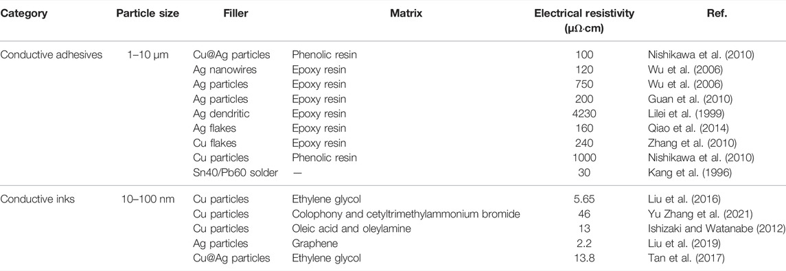
TABLE 1. Summary of some reported conductive adhesives/inks.
The conductive inks are composed of metal nanoparticles such as Cu and Ag nanoparticles and organic flux such as rosin, alcohol, and oleic acid. With low viscosity and low surface tension, the conductive inks are able to fill the microvias with large depth-to-diameter ratios (Das et al., 2008). Due to the size effect and large surface area ratio, metal nanoparticles and microparticles can form metallurgical bonds with each other at a temperature much below the melting point of bulk metals (Buffat and Borel, 1976; Yang et al., 2021a). Usually, these conductive inks are sintered at the temperature above 220°C. At this temperature, the organic fluxes in the conductive inks will decompose, and the metal particles could form sintering necks with each other, leading to a better conductivity.
In the research studies of metal particles in the fillers, Liu et al. (2016) prepared Cu nanoparticles with 30 nm diameter in a polyhydric alcohol solution and mixed them with ethylene glycol. After sintering at 260°C for 5 min, the as-prepared conductive ink obtained a resistivity of only 5.65 μΩ·cm. Tan et al. (2017) developed a conductive ink of Cu–Ag core–shell nanoparticles with 50 nm diameter. The ink obtained a resistivity of 13.8 μΩ·cm after sintering at 150°C for 60 min. Li et al. (2018) developed a Cu nanoparticle ink, which showed a resistivity of 4.37 μΩ·cm after sintering at 150°C for 60 min. Liu et al. (2019) developed a conductive ink of mixed graphene and Ag nanoparticles with a diameter of 10 nm. The ink obtained a conductivity as low as 2.2 μΩ·cm after sintering at 150°C for 60 min.
In the research studies of organic fluxes in the fillers, Zhang Y. et al. (2021) prepared a Cu nanoparticle ink with mixed fluxes of colophony and cetyltrimethylammonium bromide (CTAB). After sintering at 260°C for 30 min, the ink forms a conductive sheet with a resistivity of 46 μΩ·cm. Zhang Y. et al. (2021) found that the mixed flux of organic acid and surfactant could effectively promote the decomposition of cupric oxides during the sintering process. Ishizaki and Watanabe (2012) developed another mixed flux of oleic acid and oleylamine and found that the cupric oxides can be removed by annealing at 300°C, and the resistivity of the sintered sheet was only 13 μΩ·cm.
Microvia Filling Performance of Metal Nano/Microparticle Conductive Fillers
With the development of metal nano/microparticle conductive fillers, many research studies have been carried out to explore their performance in microvia filling.
In terms of hard substrates, the filling technique was mainly performed on through-glass vias (TGVs), through-silicon vias (TSVs), through-ceramic vias (TCVs), and through-resin vias (TRVs). Khorramdel and Mäntysalo (2016) tried to fill blind vias on silicon substrates with Ag nanoparticle paste. The resistivity of the filled vias was 2–4 orders of magnitude higher than that of bulk copper. Iwai et al. (2018a), Iwai et al. (2018b), and Iwai et al. (2019) in Fujitsu Laboratory filled TGVs in a multi-layer glass package substrate with copper paste and sintered them by a vacuum hot-pressing machine. The single hole resistance was 5.2 mΩ, and the resistivity was 0.26 μΩ·cm. Bach et al. (2018) tried to fill the vias and blind vias on ceramic substrates with Cu and Ag pastes. The compactness of the filled vias reached 95%, and the resistance of the sintered vias reached 30 μΩ. Yang T. H. et al. (2017) used silver nanoparticle paste to fill TSVs. By using the inkjet printing technology, the aspect ratio of the filled vias can be increased to 5:1, with a diameter of only 25 μm. The resistivity of the filled vias was less than 400 μΩ·cm.
In terms of flexible substrates such as polyimide (PI) and polyethylene terephthalate (PET), Falat et al. (2011) used inkjet printing technology to print Ag nanoparticle paste in 4–10 nm diameter into the vias on polyimide substrates. After sintering at 250°C for 30 min, the resistivity of the filled vias reached 4.5 μΩ·cm, which was very close to that of bulk silver (1.55 μΩ·cm). Chu et al. (2019) filled vias on polyimide substrates with a hybrid paste of mixed Cu microparticles and nanoparticles. After curing the paste with intense pulsed light, the filled vias reached a resistivity of 7.79 μΩ·cm, which was 4.45 times that of bulk copper. Quack et al. (2013) filled Ag nanoparticles into TSVs and aligned the vias toward each other under hot pressing to realize the bonding of two dies. The resistivity of a single via was less than 200 μΩ·cm. Das et al. (2008) used the pastes of Cu microparticles, low-melting-point alloy (LMPA) microparticles, and Ag microparticles to fill microvias with 75 μm diameter on a rosin substrate. The three pastes showed the resistivities of 500 μΩ·cm, 50 μΩ·cm, and 20 μΩ·cm, respectively. By mixing the Ag microparticles with Ag nanometers, the resistivity was further decreased to 10 μΩ·cm.
Table 2 shows a summary of the reported microvia filling performance of metal nano/microparticle conductive fillers. Compared with the conventional screen printing or scraping printing method, the inkjet printing method has a better filling capability for smaller and deeper vias and saves material.
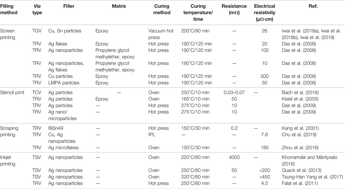
TABLE 2. Summary of the reported microvia filling performance of metal nano/microparticle conductive adhesives/inks.
It can be found that the reported resistivity of the filled microvias with metal nano/microparticles is still much higher than that of bulk metals. This is because there are still a large number of voids in the sintered structure of metal particles in the microvias. In a conventional hot-pressing process of metal particles, the gaps between the metal particles can be gradually reduced or closed under the external pressure, so that the sintered particles could form a compact structure to achieve the properties close to those of bulk metal. During the sintering process of microvias filled with metal particles, as the external pressure can hardly transfer to the particles inside the microvias, the voids between the particles can hardly be closed, resulting in a porous sintering structure with poor properties. The structure is similar to the sintered metal particles in the pressureless condition. How to achieve compact sintering of metal particles in microvias becomes a main obstacle for this technique.
This question might be solved by the design of particles with mixed sizes and densely prefill method. Through the design of particles with mixed sizes, the small particles could fill the gaps between large particles, which is an effective way to increase the overall density of sintered metal particles. By increasing the solid content in the conductive ink, and repeatedly compacting the inks in the vias several times before sintering, the metal particles in the via could also reach higher density. These dense filling methods could increase the feasibility of microvia filling with metal particles in electronics manufacturing.
Discussion
Although various research studies have been carried out to explore the synthesis and properties of metal nano/microparticle conductive adhesive/inks, their applications in microvia filling are still preliminary. For the traditional electroplating microvia filling technology, the organic additives including the accelerator, inhibitor, and leveling agent are essential components to control the diffusion and deposition processes of cupric ions at different positions of the vias. A higher bottom deposition rate than the surface deposition rate is required to realize the bottom-up filling mode and obtain a void-less filling structure (Tao et al., 2020). In comparison, the filling technology based on metal particle adhesives/inks directly injects the conductive fillers into the vias. This method shows the advantages of simpler process and higher efficiency. However, the gaps between the metal particles will leave many small cavities in the vias. The shrinkage, oxidation, and interface resistance of metal particle fillers will also influence the overall resistance of the filled vias. Therefore, the resistivity of the filled vias will be higher than that of bulk metals. Here, we would like to raise some representative research focuses of this technique, which to our knowledge have relatively high interest and importance.
Design of Filling Material
At present, Cu and Ag nanoparticle pastes are the most widely used fillers for microvia filling. Ag particle pastes have been widely used in die bond due to their high thermal conductivity (Zhang Z. et al., 2021). As fillers of microvias, the use of Ag particles is limited by their poor electromigration resistance (Kang et al., 2001). In comparison, Cu particles are more resistant to electromigration and cheaper. However, Cu particles are easily oxidized in air, and the cupric oxides are non-conductive and will hinder the sintering process of Cu particles. Some studies attempted to coat the Cu particles with organic protective agents such as polyvinyl pyrrolidone (Sampath et al., 2014), gelatin, ethanolamine, and oleylamine (Ben Aissa et al., 2015). Some researchers attempted to replace Ag/Cu particles with other conductive particles, such as Sn-coated Cu particles (Kang et al., 1998; Yoon et al., 2020) and Ag-coated Cu particles (Yu et al., 2017; Yang et al., 2021c). Due to the low melting point of Sn, the Sn-coated Cu particles can be sintered at lower temperature. The Ag-coated Cu particles have a silver protective layer to prevent the oxidation of Cu, and therefore, the particles could achieve better electrical performance and filling capability for deep vias. The development of metal particles with combined sintering property, oxidation resistance, electromigration resistance, economy, and facile preparation is still an important research topic.
Development of Filling Method
The filling method has a strong impact on the filling performance of the vias. The traditional screen-printing method provides an easy way to fill vias and grooves. However, the method shows relatively poor positioning accuracy and resolution (∼30 μm) and is not suitable for filling vias with small apertures. The suitable viscosity of the paste for screen printing is in a narrow range between 0.5 and 5 Pa·s, as the paste with higher viscosity is difficult to penetrate into the vias (Krzeminski et al., 2018). In comparison, the inkjet printing technology has a higher resolution and is more suitable for filling vias with small apertures. However, the method is prone to nozzle clogging and printing defects such as coffee rings or satellite dropping (Yang Q. et al., 2017). The inks for inkjet printing require a lower viscosity between 0.001 and 0.1 Pa·s, a surface tension between 15 and 25 mN/m, and a small particle size at nanometer scale (Cano-Raya et al., 2019). Some other advanced filling technologies have also been developed in recent years, such as aerosol jetting and extrusion printing. The aerosols for aerosol jetting technology are generated by pneumatic or ultrasonic atomization of inks, with particle sizes less than 0.2 µm. Carried by gas at high speed, the aerosols can be deposited into holes with a feature size below 10 µm and a standoff height up to 10 mm. Using the method, Renn et al. (2013) filled silver epoxy into TSVs with a depth of 300 μm and diameter of 50 μm, and a resistivity of only 5 μΩ·cm was obtained. The extrusion printing is another kind of pressure-assisted printing method, and the viscosity of the ink is relatively high (30–6 × 10⁷ mPa·s). The method is mostly used in additive manufacturing with poor resolution and is suitable for filling vias with large apertures (Yang and Fan, 2020). In addition to the above, other printing technologies such as dielectrophoretic printing, pyroelectrodynamic printing, and piezoelectric printing are expected to be used for microvia filling with metal particle inks (Mondal and McMurtrey, 2020), but relevant studies are rarely reported at present.
For microvias filled with metal particles, the density of the sintered structure is the key to its performance. As revealed by the permeation threshold theory (Aradhana et al., 2020), there is a critical concentration of conductive fillers. Above this concentration, the electrical conductivity will suddenly increase. Mixing the particles with different sizes and increasing the solid content in the particle paste are effective ways to increase the density. How to further improve the filling compactness is still of great importance for this technique.
Reducing the Sintering/Curing Temperature
As many organic substrates such as polyimide, polycarbonate (PC), and polyethylene terephthalate (PET) are sensitive to temperature, how to reduce the sintering/curing temperature of metal particle–based conductive adhesives/inks becomes an obstacle for their usage. New methods such as microwave flash sintering (Agrawal, 2006; Perelaer et al., 2009), intense pulsed light sintering (Jang et al., 2020), laser sintering (Yang et al., 2021b), electrical sintering (Allen et al., 2008), and chemical sintering (Magdassi et al., 2010) have been developed. Using nanosecond-pulsed ultraviolet laser sintering of Cu nanoparticles, Yang et al. (2021b) fabricated circuits on the polyimide substrate with a resistivity of 15 μΩ·cm. The microwave flash sintering utilizes the inductive coupling between conductive particles and microwave radiation to selectively sinter metal particles. Through microwave flash sintering of Ag nanoparticles, Perelaer et al. (2009) obtained silver circuits with a resistivity of 30 μΩ·cm. The pulsed light sintering technology utilizes the synergistic effect of opto-chemical and opto-thermal phenomena, which shortens the sintering time of metal particles to a few milliseconds and thereby reduces the oxidation of the metal particle and the damage to the substrates (Kim et al., 2009). Through multi-pulsed light sintering of the Cu nanoparticle ink, Ryu et al. (2016) prepared a conductive sheet with a conductivity of only 3.81 μΩ·cm.
On the contrary, for those temperature-insensitive substrates such as glass and ceramics substrates, the metal particle fillers could be sintered at higher temperature to obtain a more compact sintering structure with better properties. These new types of substrates may become the field where the metal particle microvia filling technology applies in the future.
Author Contributions
GY wrote the original draft. SL and ZL investigated the data. SL visualized the data. YZ and CC supervised the work and acquired the funding.
Conflict of Interest
The authors declare that the research was conducted in the absence of any commercial or financial relationships that could be construed as a potential conflict of interest.
Publisher’s Note
All claims expressed in this article are solely those of the authors and do not necessarily represent those of their affiliated organizations, or those of the publisher, the editors, and the reviewers. Any product that may be evaluated in this article, or claim that may be made by its manufacturer, is not guaranteed or endorsed by the publisher.
Acknowledgments
We acknowledge the support of the National Natural Science Foundation of China (Grant No. 61874155), National Key R&D Program of China (2018YFE0204601), Key Research and Development Program of Guangdong Province (2020B0101290001), Guangdong Basic and Applied Basic Research (2021A1515011642), and Open Project of the State Key Laboratory of Advanced Materials and Electronic Components (FHR-JS-202011005).
References
Agrawal, D. (2006). Microwave Sintering of Ceramics, Composites and Metallic Materials, and Melting of Glasses. Trans. Indian Ceram. Soc. 65 (3), 129–144. doi:10.1080/0371750X.2006.11012292
Allen, M. L., Aronniemi, M., Mattila, T., Alastalo, A., Ojanperä, K., Suhonen, M., et al. (2008). Electrical Sintering of Nanoparticle Structures. Nanotechnology 19 (17), 175201. doi:10.1088/0957-4484/19/17/175201
Andoh, D., Tomita, Y., Nakamura, T., and Echigo, F. (2022). “The Progress of the ALIVH Substrate,” in 52nd Electronic Components and Technology Conference 2002. (Cat. No.02CH37345), San Diego, CA, USA, 1419–1424.
Aradhana, R., Mohanty, S., and Nayak, S. K. (2020). A Review on Epoxy-Based Electrically Conductive Adhesives. Int. J. Adhes. Adhesives 99, 102596. doi:10.1016/j.ijadhadh.2020.102596
Bach, H. L., Yu, Z., Letz, S., Bayer, C. F., Waltrich, U., Schletz, A., et al. (2018). “Vias in DBC Substrates for Embedded Power Modules,” in CIPS 2018; 10th International Conference on Integrated Power Electronics Systems (Stuttgart, Germany: VDE), 1–5.
Ben Aissa, M. A., Tremblay, B., Andrieux-Ledier, A., Maisonhaute, E., Raouafi, N., and Courty, A. (2015). Copper Nanoparticles of Well-Controlled Size and Shape: a New advance in Synthesis and Self-Organization. Nanoscale 7 (7), 3189–3195. doi:10.1039/c4nr06893a
Buffat, P., and Borel, J.-P. (1976). Size Effect on the Melting Temperature of Gold Particles. Phys. Rev. A. 13 (6), 2287–2298. doi:10.1103/PhysRevA.13.2287
Cano-Raya, C., Denchev, Z. Z., Cruz, S. F., and Viana, J. C. (2019). Chemistry of Solid Metal-Based Inks and Pastes for Printed Electronics - A Review. Appl. Mater. Today 15, 416–430. doi:10.1016/j.apmt.2019.02.012
Chu, J.-H., Joo, S.-J., and Kim, H.-S. (2019). Development of a Via-Hole Connection Process via Intense Pulsed Light Sintering with Cu micro/Ag Nano-Hybrid Ink for a Multi-Layered Flexible Printed Circuit Board. Thin Solid Films 680, 1–11. doi:10.1016/j.tsf.2019.04.015
Das, R. N., Egitto, F. D., Lauffer, J. M., Poliks, M. D., and Markovich, V. R. (2009). “Influence of Carbon, Metal-Coated Polymer, and Nano Powders on Sintering and Electrical Performance of Nano-Micro-Filled Conducting Adhesives for Z-axis Interconnections,” in 2009 IEEE 59th Electronic Components and Technology Conference (Ectc 2009) (San Diego, CA: IEEE), 180–187. doi:10.1109/ectc.2009.5074013
Das, R. N., Egitto, F. D., and Markovich, V. R. (2008). Nano‐ and Micro‐filled Conducting Adhesives for Z‐axis Interconnections: New Direction for High‐speed, High‐density, Organic Microelectronics Packaging. Circuit World 34 (1), 3–12. doi:10.1108/03056120810848743
Falat, T., Felba, J., Moscicki, A., and Borecki, J. (2011). “Nano-silver Inkjet Printed Interconnections through the Microvias for Flexible Electronics,” in 2011 11th IEEE International Conference on Nanotechnology (Portland, OR: IEEE), 473–477.
Fukuoka, Y., Oguma, T., and Tahara, Y. (1998). “New High Density Substrates With Buried Bump Interconnection Technology (B(2)it (TM)) - Design Features of Electrical and Thermal Performance With the Actual Applications,” in Proceedings of 1998 International Symposium on Microelectronics (San Diego, Ca: SPIE-INT SOC Optical Engineering), 405–412.
Goto, K., Oguma, T., and Fukuoka, Y. (1998). “High Density Printed Circuit Board Using B/sup 2/it/sup TM/Technology,” in 2nd 1998 IEMT/IMC Symposium (IEEE Cat. No.98EX225), Sonic City-Omiya, Tokyo Japan, 15-17 April 1998, 316–320.
Guan, Y., Chen, X., Li, F., and Gao, H. (2010). Study on the curing process and shearing tests of die attachment by Ag-epoxy electrically conductive adhesive. Int. J. Adhes. Adhesives 30 (2), 80–88. doi:10.1016/j.ijadhadh.2009.09.003
Ishizaki, T., and Watanabe, R. (2012). A New One-Pot Method for the Synthesis of Cu Nanoparticles for Low Temperature Bonding. J. Mater. Chem. 22 (48), 25198–25206. doi:10.1039/C2JM34954J
Iwai, T., Sakai, T., Mizutani, D., Sakuyama, S., Iida, K., Inaba, T., et al. (2018a). “A Novel Inorganic Substrate by Three Dimensionally Stacked Glass Core Technology,” in 2018 IEEE 68th Electronic Components and Technology Conference (ECTC) (San Diego, CA: IEEE), 1987–1992. doi:10.1109/ectc.2018.00298
Iwai, T., Sakai, T., Mizutani, D., Sakuyama, S., Iida, K., Inaba, T., et al. (2018b). “Glass Multilayer Package Substrate Using Conductive Paste via Connection,” in 2018 IEEE CPMT Symposium Japan (ICSJ) (Kyoto, Japan: IEEE), 105–108.
Iwai, T., Sakai, T., Mizutani, D., Sakuyama, S., Iida, K., Inaba, T., et al. (2019). “Multilayer Glass Substrate with High Density via Structure for All Inorganic Multi-Chip Module,” in 2019 IEEE 69th Electronic Components and Technology Conference (ECTC) (Las Vegas, NV: IEEE), 1952–1957. doi:10.1109/ectc.2019.00301
Jang, Y.-R., Joo, S.-J., Chu, J.-H., Uhm, H.-J., Park, J.-W., Ryu, C.-H., et al. (2020). A Review on Intense Pulsed Light Sintering Technologies for Conductive Electrodes in Printed Electronics. Int. J. Precis. Eng. Manuf.-Green Tech. 8, 327–363. doi:10.1007/s40684-020-00193-8
Kang, S. K., Buchwalter, S. L., LaBianca, N. C., Gelorme, J., Purushothaman, S., Papathomas, K., et al. (2001). Development of Conductive Adhesive Materials for via Fill Applications. IEEE Trans. Comp. Packag. Technol. 24 (3), 431–435. doi:10.1109/6144.946490
Kang, S. K., Rai, R., and Purushothaman, S. (1996). “Development of High Conductivity lead (Pb)-free Conducting Adhesives,” in 1996 Proceedings 46th Electronic Components and Technology Conference (Orlando, FL: IEEE), 565–570.
Kang, S. K., Rai, R. S., and Purushothaman, S. (1998). Development of High Conductivity lead (Pb)-free Conducting Adhesives. IEEE Trans. Comp. Packag., Manufact. Technol. A. 21 (1), 18–22. doi:10.1109/95.679027
Khorramdel, B., and Mäntysalo, M. (2016). Fabrication and Electrical Characterization of Partially Metallized Vias Fabricated by Inkjet. J. Micromech. Microeng. 26 (4), 045017. doi:10.1088/0960-1317/26/4/045017
Kim, H.-S., Dhage, S. R., Shim, D.-E., and Hahn, H. T. (2009). Intense Pulsed Light Sintering of Copper Nanoink for Printed Electronics. Appl. Phys. A. 97 (4), 791–798. doi:10.1007/s00339-009-5360-6
Kisiel, R., Borecki, J., Kozioł, G., and Felba, J. (2005). Conductive Adhesives for through Holes and Blind Vias Metallization. Microelectronics Reliability 45 (12), 1935–1940. doi:10.1016/j.microrel.2005.03.005
Krzeminski, J., Kanthamneni, A., Wagner, D., Detert, M., Schmidt, B., and Jakubowska, M. (2018). Microscale Hybrid Flexible Circuit Printed with Aerosol Jet Technique. IEEE Trans. Nanotechnology 17 (5), 979–984. doi:10.1109/TNANO.2018.2841639
Li, J., Shi, T., Feng, C., Liang, Q., Yu, X., Fan, J., et al. (2018). The Novel Cu Nanoaggregates Formed by 5 Nm Cu Nanoparticles with High Sintering Performance at Low Temperature. Mater. Lett. 216, 20–23. doi:10.1016/j.matlet.2017.12.094
Lilei Ye, Y., Zonghe Lai, L., Johan Liu, L., and Tholen, A. (1999). Effect of Ag Particle Size on Electrical Conductivity of Isotropically Conductive Adhesives. IEEE Trans. Electron. Packag. Manufact. 22 (4), 299–302. doi:10.1109/6104.816098
Liu, J., Chen, H., Ji, H., and Li, M. (2016). Highly Conductive Cu-Cu Joint Formation by Low-Temperature Sintering of Formic Acid-Treated Cu Nanoparticles. ACS Appl. Mater. Inter. 8 (48), 33289–33298. doi:10.1021/acsami.6b10280
Liu, P., He, W.-q., and Lu, A.-x. (2019). Preparation of Low-Temperature Sintered High Conductivity Inks Based on Nanosilver Self-Assembled on Surface of Graphene. J. Cent. South. Univ. 26 (11), 2953–2960. doi:10.1007/s11771-019-4227-z
Magdassi, S., Grouchko, M., Berezin, O., and Kamyshny, A. (2010). Triggering the Sintering of Silver Nanoparticles at Room Temperature. ACS Nano 4 (4), 1943–1948. doi:10.1021/nn901868t
Mondal, K., and McMurtrey, M. D. (2020). Present Status of the Functional Advanced Micro-, Nano-Printings - a Mini Review. Mater. Today Chem. 17, 100328. doi:10.1016/j.mtchem.2020.100328
Nakase, H., Fujii, T., Oshima, S., Oguma, H., Kameda, S., Isota, Y., et al. (2008). “Evaluation of High Frequency Characteristics of ALIVH Substrate for 60 GHz RF Modules,” in 2006 8th Electronics Packaging Technology Conference (EPTC 2006) (Singapore: IEEE), 639–642. doi:10.1109/eptc.2006.342788
Nedfors, N., Primetzhofer, D., Wang, L., Lu, J., Hultman, L., and Jansson, U. (2015). Characterization of Magnetron Sputtered Cr-B and Cr-B-C Thin Films for Electrical Contact Applications. Surf. Coat. Techn. 266, 167–176. doi:10.1016/j.surfcoat.2015.02.037
Nishikawa, H., Mikami, S., Miyake, K., Aoki, A., and Takemoto, T. (2010). Effects of Silver Coating Covered with Copper Filler on Electrical Resistivity of Electrically Conductive Adhesives. Mater. Trans. 51, 1785–1789. doi:10.2320/matertrans.MJ201020
Nothdurft, P., Riess, G., and Kern, W. (2019). Copper/Epoxy Joints in Printed Circuit Boards: Manufacturing and Interfacial Failure Mechanisms. Materials 12, 550. doi:10.3390/ma12030550
Ochi, S., Echigo, F., Nakamura, T., Tomita, Y., and Andoh, D. (2002). “A Study of Advanced ALIVH(R) Interconnection Technology,” in 2002 Proceedings. 8th International Advanced Packaging Materials Symposium (Cat. No.02TH8617), Stone Mountain, GA, USA, 3-6 March 2002, 356–361.
Perelaer, J., Klokkenburg, M., Hendriks, C. E., and Schubert, U. S. (2009). Microwave Flash Sintering of Inkjet-Printed Silver Tracks on Polymer Substrates. Adv. Mater. 21 (47), 4830–4834. doi:10.1002/adma.200901081
Qiao, W., Bao, H., Li, X., Jin, S., and Gu, Z. (2014). Research on Electrical Conductive Adhesives Filled with Mixed Filler. Int. J. Adhes. Adhesives 48, 159–163. doi:10.1016/j.ijadhadh.2013.07.001
Quack, N., Sadie, J., Subramanian, V., and Wu, M. C. (2013). “Through Silicon Vias and Thermocompression Bonding Using Inkjet-Printed Gold Nanoparticles for Heterogeneous MEMS Integration,” in 2013 Transducers & Eurosensors XXVII: The 17th International Conference on Solid-State Sensors, Actuators and Microsystems (TRANSDUCERS & EUROSENSORS XXVII), Barcelona, Spain, 16-20 June 2013, 834–837.
Renn, M. J., Christenson, K. K., Giroux, D., and Blazej, D. (2013). “Aerosol Jet® Printing of Conductive Epoxy for 3D Packaging,” in Pan Pacific Microelectronics Symposium, 1–7.
Ryu, C.-H., Joo, S.-J., and Kim, H.-S. (2016). Two-step Flash Light Sintering of Copper Nanoparticle Ink to Remove Substrate Warping. Appl. Surf. Sci. 384, 182–191. doi:10.1016/j.apsusc.2016.05.025
Sampath, M., Vijayan, R., Tamilarasu, E., Tamilselvan, A., and Sengottuvelan, B. (2014). Green Synthesis of Novel Jasmine Bud-Shaped Copper Nanoparticles. J. Nanotechnology 2014, 1–7. doi:10.1155/2014/626523
Suzuki, T., Tomekawa, S., Ogawa, T., Andoh, D., Tanahashi, M., and Ishida, T. (2001). “Interconnection Technique of ALIVH/sup (R)/Substrate,” in Proceedings International Symposium on Advanced Packaging Materials Processes, Properties and Interfaces (IEEE Cat. No.01TH8562), 23–28.
Szałatkiewicz, J. (2016). Metals Recovery from Artificial Ore in Case of Printed Circuit Boards, Using Plasmatron Plasma Reactor. Materials (Basel) 9 (8), 683. doi:10.3390/ma9080683
Tan, S., Zu, X., Yi, G., and Liu, X. (2017). Synthesis of Highly Environmental Stable Copper-Silver Core-Shell Nanoparticles for Direct Writing Flexible Electronics. J. Mater. Sci. Mater. Electron. 28, 15899–15906. doi:10.1007/s10854-017-7485-2
Tao, P., Chen, Y., Cai, W., and Meng, Z. (2020). Effect of Copper Sulfate and Sulfuric Acid on Blind Hole Filling of HDI Circuit Boards by Electroplating. Materials 14, 85. doi:10.3390/ma14010085
Timsit, R. S. (2013). “Electrical Contacts: Scientific Fundamentals,” in Encyclopedia of Tribology. Editors Q.J. Wang, and Y.-W. Chung (Boston, MA: Springer US), 903–905. doi:10.1007/978-0-387-92897-5_429
Wu, H. P., Liu, J. F., Wu, X. J., Ge, M. Y., Wang, Y. W., Zhang, G. Q., et al. (2006). High Conductivity of Isotropic Conductive Adhesives Filled with Silver Nanowires. Int. J. Adhes. Adhesives 26 (8), 617–621. doi:10.1016/j.ijadhadh.2005.10.001
Yang, G., Lai, H., Lin, W., Tong, J., Cao, J., Luo, J., et al. (2021a). A Quantitative Model to Understand the Microflow-Controlled Sintering Mechanism of Metal Particles at Nanometer to Micron Scale. Nanotechnology 32 (50), 505721. doi:10.1088/1361-6528/ac232d
Yang, G., Xu, G., Li, Q., Zeng, Y., Zhang, Y., Hao, M., et al. (2021b). Understanding the Sintering and Heat Dissipation Behaviours of Cu Nanoparticles during Low-Temperature Selective Laser Sintering Process on Flexible Substrates. J. Phys. D: Appl. Phys. 54 (37), 375304. doi:10.1088/1361-6463/ac0d73
Yang, G., Zou, Q., Wang, P., Lai, H., Lai, T., Zeng, X., et al. (2021c). Towards Understanding the Facile Synthesis of Well-Covered Cu-Ag Core-Shell Nanoparticles from a Complexing Model. J. Alloys Compd. 874, 159900. doi:10.1016/j.jallcom.2021.159900
Yang, P., and Fan, H. J. (2020). Inkjet and Extrusion Printing for Electrochemical Energy Storage: A Minireview. Adv. Mater. Technol. 5 (10), 2000217. doi:10.1002/admt.202000217
Yang, Q., Li, H., Li, M., Li, Y., Chen, S., Bao, B., et al. (2017). Rayleigh Instability-Assisted Satellite Droplets Elimination in Inkjet Printing. ACS Appl. Mater. Inter. 9 (47), 41521–41528. doi:10.1021/acsami.7b11356
Yang, T. H., Guo, Z. L., Fu, Y. M., Cheng, Y. T., Song, Y. F., and Wu, P. W. (2017). “A Low Temperature Inkjet Printing and Filling Process for Low Resistive Silver TSV Fabrication in a SU-8 Substrate,” in MEMS: 2017 IEEE 30th International Conference on Micro Electro Mechanical Systems (Las Vegas, NV: IEEE), 749–752. doi:10.1109/memsys.2017.7863516
Yoon, J.-W., Bae, S., Lee, B.-S., and Jung, S.-B. (2020). Bonding of Power Device to Ceramic Substrate Using Sn-Coated Cu Micro Paste for High-Temperature Applications. Appl. Surf. Sci. 515, 146060. doi:10.1016/j.apsusc.2020.146060
Yu, X., Li, J., Shi, T., Cheng, C., Liao, G., Fan, J., et al. (2017). A green Approach of Synthesizing of Cu-Ag Core-Shell Nanoparticles and Their Sintering Behavior for Printed Electronics. J. Alloys Compd. 724, 365–372. doi:10.1016/j.jallcom.2017.07.045
Zhang, R., Lin, W., Lawrence, K., and Wong, C. P. (2010). Highly Reliable, Low Cost, Isotropically Conductive Adhesives Filled with Ag-Coated Cu Flakes for Electronic Packaging Applications. Int. J. Adhes. Adhesives 30 (6), 403–407. doi:10.1016/j.ijadhadh.2010.01.004
Zhang, Y., Cao, P., Lin, W., Liu, Q., Chen, Z., Cao, J., et al. (2021a). Synergy Effect of Mixed Sintering Accelerator on the Deoxidation and Sintering Property Improvement of Cu Nanoparticles at Low Temperature. Appl. Phys. A. 127 (10), 783. doi:10.1007/s00339-021-04924-9
Zhang, Z., Chen, C., Suetake, A., Hsieh, M.-C., Iwaki, A., and Suganuma, K. (2021b). Pressureless and Low-Temperature Sinter-Joining on Bare Si, SiC and GaN by a Ag Flake Paste. Scripta Materialia 198, 113833. doi:10.1016/j.scriptamat.2021.113833
Keywords: microvia filling, metal particle fillers, conductive inks, sintering, vertical interconnection
Citation: Yang G, Luo S, Li Z, Zhang Y and Cui C (2022) A Mini Review on the Microvia Filling Technology Based on Printed Metal Nano/Microparticles. Front. Mater. 9:860710. doi: 10.3389/fmats.2022.860710
Received: 23 January 2022; Accepted: 08 March 2022;
Published: 30 March 2022.
Edited by:
Wenzhuo Wu, Purdue University, United StatesReviewed by:
Roberto Bernasconi, Politecnico di Milano, ItalyCopyright © 2022 Yang, Luo, Li, Zhang and Cui. This is an open-access article distributed under the terms of the Creative Commons Attribution License (CC BY). The use, distribution or reproduction in other forums is permitted, provided the original author(s) and the copyright owner(s) are credited and that the original publication in this journal is cited, in accordance with accepted academic practice. No use, distribution or reproduction is permitted which does not comply with these terms.
*Correspondence: Yu Zhang, emhhbmd5dUBnZHV0LmVkdS5jbg==; Chengqiang Cui, Y3FjdWlAZ2R1dC5lZHUuY24=