 Ziheng Wang
 Zehao Lin
 Mengwei Si
 Peide D. Ye
94% of researchers rate our articles as excellent or good
Learn more about the work of our research integrity team to safeguard the quality of each article we publish.
Find out more
ORIGINAL RESEARCH article
Front. Mater., 04 May 2022
Sec. Semiconducting Materials and Devices
Volume 9 - 2022 | https://doi.org/10.3389/fmats.2022.850451
This article is part of the Research Topic2022 Retrospective: Semiconducting Materials and DevicesView all 5 articles
Oxide semiconductors have attracted revived interest for complementary metal–oxide–semiconductor (CMOS) back-end-of-line (BEOL) compatible devices for monolithic 3-dimensional (3D) integration. To obtain a high-quality oxide/semiconductor interface and bulk semiconductor, it is critical to enhance the performance of oxide semiconductor transistors. Atomic layer-deposited (ALD) indium oxide (In2O3) has been reported with superior performance such as high drive current, high mobility, steep subthreshold slope, and ultrathin channel. In this work, the interface and bulk traps in the MOS gate stack of ALD In2O3 transistors are systematically studied by using the C–V and conductance method. A low EOT of 0.93 nm is achieved directly from the accumulation capacitance in C–V measurement, indicating a high-quality gate oxide and oxide/semiconductor interface. Defects in bulk In2O3 with energy levels in the subgap are confirmed to be responsible for the conductance peak in GP/ω versus ω curves by TCAD simulation of C–V and G–V characteristics. A high n-type doping of 1×10²⁰/cm3 is extracted from C–V measurement. A high subgap density of states (DOS) of 3.3×1020 cm−3 eV−1 is achieved using the conductance method, which contributes to the high n-type doping and high electron density. The high n-type doping further confirms the capability of channel thickness scaling because the charge neutrality level aligns deeply inside the conduction band.
Oxide semiconductors (Nomura et al., 2004; Kamiya et al., 2010) are widely used in thin-film transistors (TFTs) as channel materials and are considered as promising candidates for complementary metal–oxide–semiconductor (CMOS) back-end-of-line (BEOL) compatible transistors for monolithic three-dimensional (3D) integration. Indium oxide (In2O3) (Si et al., 2021a; Si et al., 2021b; Si et al., 2021c; Si et al., 2021d) or doped In2O3 (Matsubayashi et al., 2015; Li et al., 2019; Chakraborty et al., 2020; Fujiwara et al., 2020; Li et al., 2020; Samanta et al., 2020; Han et al., 2021) deposited by both sputtering and atomic layer deposition (ALD) are being investigated due to high mobility, low variability, wide bandgap, and high stability. Recently, ALD-based oxide semiconductors have attracted much attention due to the atomically smooth surface, low thermal budget, precise thickness control down to sub-1 nm, and capability of depositing a conformal film on 3D structures, achieving high-performance devices with maximum drain current >2 A/mm, high electron mobility >100 cm2/Vs, high on/off ratio > 1010, and near-ideal subthreshold slope (SS) down to 63.8 mV/dec at room temperature, making them leading candidates as channel semiconductors for monolithic 3D integration (Si et al., 2021a; Si et al., 2021b; Si et al., 2021c; Si et al., 2021d).
In2O3 has a charge neutrality level (CNL) at above 0.4 eV above the conduction band (EC). It was understood that this is the origin of high electron density and low contact resistance in an atomically thin channel (Si et al., 2021a). Such high electron density is directly associated with the subgap density of states (DOS) in In2O3. Meanwhile, in oxide semiconductor-based transistors, the electrical performance and reliability are closely connected with the subgap DOS over the bandgap. Therefore, it is important to extract and study the impact of trap states. However, the interface and bulk traps in ultrathin ALD oxide semiconductor devices have not been systematically studied. Capacitance–voltage (C–V) measurements and the conductance method are commonly used to extract interface trap density (Dit) in MOS capacitors, which is used to evaluate the characteristics of interface and bulk traps in ALD In2O3 MOS capacitors.
In this work, the interface and bulk traps in the MOS gate stack of ALD In2O3 transistors are systematically studied by using the C–V and conductance method. ALD In2O3 transistors and MOS capacitors with 3.5 nm HfO2 as the gate insulator and 3.5 nm In2O3 as the channel semiconductor are fabricated, achieving a low equivalent oxide thickness (EOT) of 0.93 nm, indicating a high-quality gate oxide and oxide/semiconductor interface. The C–V and conductance method were utilized to study the properties of interface and bulk trap states in the gate stack of In2O3 transistors. A high n-type doping of 1 × 10²⁰/cm3 is achieved by C–V measurement. This is further confirmed by the high conductance peak of 7.6 × 10⁻⁶ S s/cm2, corresponding to a high subgap DOS of 3.3×1020 cm−3 eV−1, which contributes to the high n-type doping and high electron density. The high electron density is because CNL aligns deeply inside the EC, which is speculated to be related to In atoms, thus In-based semiconductors tend to have a high electron density. TCAD simulation is used to study the impact of the interface traps and bulk traps on C–V curves and conductance peaks of the MOS capacitors. It is found that bulk traps across the ultrathin body contribute to the large frequency dispersion in high VGS and the large conductance peak in GP/ω versus ω characteristics.
Figures 1A,B show the schematic diagram of an ALD In2O3 transistor and an MOS capacitor with the same gate stack fabricated together with the transistor. The gate stack contains 40 nm Ni as the gate metal, 3.5 nm HfO2 as the gate insulator, 3.5 nm In2O3 as the semiconductor channel, and 80 nm Ni as the source/drain (S/D) contacts. The area of MOS capacitors used in this work is 60 μm by 60 μm. The detailed fabrication process of the In2O3 transistors is similar to that used in Si et al. (2021c). The fabrication process starts with a standard cleaning of the p + Si substrate with 90 nm SiO2 grown thermally for device isolation. Then a bilayer photoresist lithography process is conducted for the sharp lift-off of the 40 nm Ni gate metal by e-beam evaporation. 3.5 nm HfO2 was then deposited by ALD at 200°C, using [(CH3)2N]4Hf (TDMAHf) and H2O as Hf and O precursors. Then, 3.5 nm In2O3 was also deposited by ALD at 225°C, using (CH3)3In (TMIn) and H2O as In and O precursors and N2 as the carrier gas. After that, 80 nm Ni was deposited by e-beam evaporation as S/D contacts, patterned by electron beam lithography. The overlap between the gate and S/D electrodes is 2 μm. The devices were annealed in O2 at 200°C for 4 min. No obvious interdiffusion between HfO2/In2O3 and In2O3/Ni is observed in a high-resolution transmission electron microscope (HRTEM), at least at the resolution of ∼nm, as demonstrated in our previous work (Si et al., 2022) using a similar process. I–V measurements were performed using a Keysight B1500 semiconductor analyzer, while C–V and conductance measurements were conducted using an Agilent E4980A LCR meter.
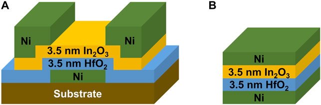
FIGURE 1. Schematic diagram of (A) an ALD In2O3 transistor with 3.5 nm In2O3 as the channel semiconductor and 3.5 nm HfO2 as the gate dielectric; (B) the gate stack capacitor fabricated together with the ALD In2O3 transistor.
The simulations were conducted on the gate stack capacitor to investigate the effects of trap states using TCAD tools. A two-dimensional gate stack capacitor, with 3.5 nm HfO2 as the gate dielectric, 3.5 nm In2O3 as the semiconductor, and Ni as the top and bottom electrodes, was used for the TCAD simulation, which is the same as the Ni/In2O3/HfO2/Ni capacitor used in the experiment. During simulation, all structural dimensions and material parameters were kept unchanged. Some typical physical models for MOS capacitor simulation were utilized. To be specific, the CVT transverse field-dependent mobility model and a lateral electric field-dependent model were used for electrons and holes by specifying CVT and FLDMOB, respectively, in the model statement, while Auger recombination was also considered by specifying Auger in the model statement. In addition, the defects model and intdefects model were also used to specify interface trap states at the In2O3/HfO2 interface and bulk trap states in the In2O3 layer, respectively. For both bulk traps and interface traps, one tail distribution of acceptor-like traps at the conduction band edge, one tail distribution of donor-like traps at the valence band edge, and one deep-level Gaussian distribution of traps were specified (Kamiya et al., 2010; Jankovic, 2012), with NTA, NTD, and NGA to determine the peak density of these three types of traps, respectively. All traps are uniformly distributed in space, for both interface and bulk traps. C–V and G–V characteristics of the MOS capacitor were simulated to investigate the impacts of interface traps and bulk traps.
Figure 2A shows the ID–VGS characteristics at VDS of 0.05 and 1 V of an ALD In2O3 transistor with a channel length (Lch) of 1 μm and a channel thickness (Tch) of 3.5 nm. The gate leakage current (IG) is also presented in Figure 2A, which is relatively high due to the highly scaled EOT, resulting in the relatively low on/off ratio and large subthreshold slope (SS). SS down to 63.8 mV/dec was achieved on ALD In2O3 transistors at room temperature, corresponding to a low Dit of 6.3 × 1011 cm−2 eV−1 (Si et al., 2021d). The on/off ratio and SS of the device can be further improved by threshold voltage (VT) engineering. Field-effect mobility (μFE) is extracted at VDS of 0.05 V using maximum gm to be 46 cm2/V⋅s. Figure 2B shows the ID–VDS characteristics at VGS from −2 to 2 V of the same ALD In2O3 transistor as in Figure 2A. A maximum drain current of 903 μA/μm is achieved at VDS of 3 V, showing well-behaved ID saturation characteristics at high VDS due to a drain side pinch-off.
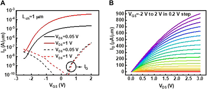
FIGURE 2. (A) ID–VGS and (B) ID–VDS characteristics of an In2O3 transistor with Lch of 1 μm and Tch of 3.5 nm, where in (A), the solid lines are ID–VGS and the dotted lines are IG–VGS curves.
The transport properties of oxide semiconductors, especially indium–gallium–zinc oxide (IGZO), are known to be closely related to the defect states in the bandgap (subgap states) (Kamiya and Hosono, 2010). Here, C–V and G–V methods were adopted to study the characteristics of these defect states in ALD In2O3 MOS capacitors. The top Ni electrode of the capacitor has no direct overlap with the p + Si substrate, and so the p + Si layer in the substrate will not show any parasitic role when measuring C–V characteristics. Figure 3A shows the C–V measurements of the gate stack capacitor fabricated together with the transistor in Figure 2, the structure of which is shown in Figure 1B. An accumulation capacitance of 3.7 μC/cm2 is achieved, corresponding to an EOT of 0.93 nm. A dielectric constant of 15 for HfO2 is achieved assuming that oxide capacitance (Cox) is close to the accumulation capacitance, suggesting a high-quality oxide/semiconductor interface. The large frequency dispersion at high VGS is because of electron generation and recombination from the subgap defect states. The C–V curve also shows a minimum capacitance of 2.0 μC/cm2 at low voltage. At low voltage, In2O3 is depleted so that the minimum capacitance can be estimated as Cox and the semiconductor capacitance (CS) in series, where CS = ϵSϵ0/Tch and ε0 is 8.85 × 10⁻¹⁴ F/cm as vacuum permittivity. As a result, ϵS of 20 is obtained, which is higher than about 8.9 by optical measurement (Hamberg and Granqvist, 1986). The overestimation of CS is caused by nonideal effects such as In2O3 at −1.5 V might not be fully depleted, Maxwell–Wagner effect, and the response from defect states.
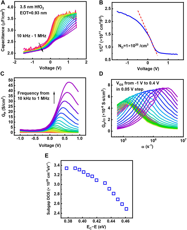
FIGURE 3. (A) C–V, (B) 1/C2 versus voltage, (C) GP versus voltage, and (D) GP/ω versus ω characteristics of the Ni/3.5 nm In2O3/3.5 nm HfO2/Ni gate stack. (E) Subgap DOS distribution extracted by using the conductance method.
The subgap defect states can be divided into two groups: shallow donors that contribute to the conducting electron or other defect states such as deep localized states (Jankovic, 2012). The doping concentration (ND) can be extracted from 1/C2 versus voltage characteristics according to
To evaluate the total density of subgap DOS, the conductance method is applied. Figure 3C shows the GP versus voltage characteristics at different frequencies measured simultaneously with the C–V curve as in Figure 3A, where GP decreases at high voltages suggesting that the impact of leakage current on GP is small compared to the impact of trap states. GP/ω versus ω characteristics are calculated from G–V data and Cox from C–V data, as shown in Figure 3D, exhibiting a high conductance peak of 7.6 × 10⁻⁶ S s/cm2, corresponding to a high subgap DOS of 1.2 × 1014 cm−2 eV−1 or 3.3 × 1020 cm−3 eV−1 normalized by Tch. Note that the conductance peaks here appear at around V = 0, so that it is not affected by the gate leakage current. Figure 3E shows the subgap DOS versus energy level extracted from GP/ω versus ω data in Figure 3D, with energy mapping obtained from the peak frequency (Brammertz et al., 2007). The conductance measurement further confirms the high subgap DOS in ALD In2O3, which contributes to the high carrier density.
Note that the high electron density in the ultrathin ALD In2O3 film is critical to achieve high ID in an ultrathin semiconducting film. In other words, semiconducting films with CNL alignment deeply inside EC are more suitable for devices with an ultrathin body in the nanometer scale. Such CNL alignment ensures a low Schottky barrier and a high carrier density, even considering the impact of quantum confinement effects. The CNL alignments of some selected semiconductor materials are plotted in Figure 4, including conventional semiconductors such as Si/Ge/III–V and oxide semiconductors such as IGZO (Mönch, 1997; Robertson and Falabretti, 2006; Ye, 2008; Robertson and Clark, 2011; Wager et al., 2012; Swallow et al., 2021). As we can see, in both conventional semiconductors and oxide semiconductors, materials with In atoms tend to have CNL closer to the vacuum level with higher electron density. Therefore, to look for materials deeper inside EC and with reasonable bandgap is the key to realize high-performance semiconducting materials with ultrathin bodies.
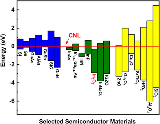
FIGURE 4. CNL alignments of the selected semiconductor materials including conventional semiconductors and oxide semiconductors.
TCAD simulations are conducted to investigate the impact of defects at the oxide/semiconductor interface and in bulk In2O3 on the C–V and G–V characteristics of ALD In2O3 MOS capacitors using the same structure as in Figure 1B. Figure 5 shows TCAD simulation results investigating the impact of interface trap states at the HfO2/In2O3 interface on C–V measurements and the conductance method. The interface trap density at the HfO2/In2O3 interface has been estimated to be 6.3 × 1011 cm−2 eV−1 with the subthreshold method (Si et al., 2021d). In this work, SS is much larger because of the impact of gate leakage, but the Dit at the HfO2/In2O3 interface is expected to be similar to the aforementioned value and independent of channel thickness because of the similar atomic configuration. For the TCAD simulation, a U-shape interface trap states distribution was specified at the HfO2/In2O3 interface of the gate stack (Schulz, 1983; Jankovic, 2012), with a minimum Dit of 1012 cm−2 eV−1 for Figures 5A,B and 1013 cm−2 eV−1 for Figures 5C,D. Acceptor-like and donor-like traps are in tail distribution at the valence band and conduction band edges, respectively. Figure 5A and Figure 5C present the simulated C–V data of the gate stack capacitor, exhibiting frequency dispersion in the depletion region and no obvious frequency dispersion in the accumulation region. Figures 5B,D show the corresponding GP/ω versus ω characteristics, showing a much lower conductance peak than the experimental data, even with quite large Dit. Both C–V and G–V simulation results confirm that interface traps at the HfO2/In2O3 interface are not the main reason for the C–V frequency dispersion in the depletion region and high conductance peak extracted from the experiments. Therefore, the frequency dispersion and high conductance peak are most likely contributed by the bulk traps inside In2O3.
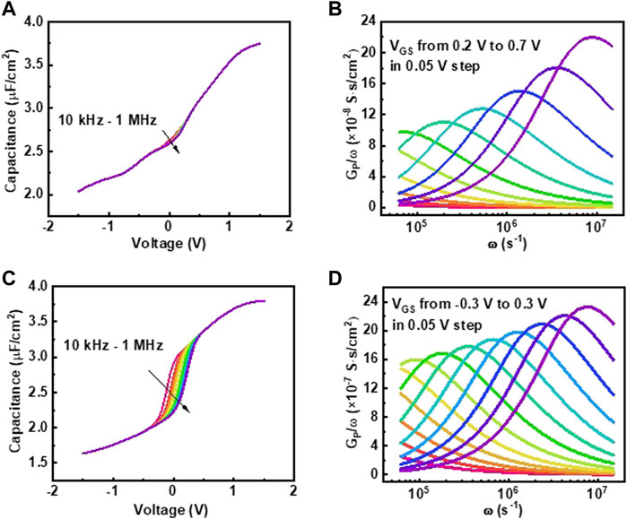
FIGURE 5. Simulated (A) C–V and (B) GP/ω versus ω characteristics of the gate stack capacitor with the same structure as in Figure 1B, using Dit of 1012 cm−2 eV−1. Simulated (C) C–V and (D) GP/ω versus ω characteristics of the gate stack capacitor with the same structure as in Figure 1B, using Dit of 1013 cm−2 eV−1.
Figure 6 shows the TCAD simulation results investigating the impact of the bulk trap states in the In2O3 layer on C–V and G–V characteristics. The bulk trap distribution in the semiconductor layer for simulation is shown in Figure 6C, considering trap states with both Gaussian and tail distributions (Kamiya et al., 2010). The bulk trap levels below mobility edge have a peak density of nearly 6×1021 cm−3 eV−1. Figure 6A shows simulated C–V characteristics of the gate stack capacitor, showing a significant frequency dispersion in the accumulation region. Figure 6B shows the corresponding GP/ω versus ω data. A high conductance peak of about 1.1 × 10⁻⁵ S∙s/cm2 can be extracted from the simulation results. Both simulated C–V characteristics and GP/ω-ω characteristics are highly consistent with the experimental results, which proves that bulk traps of more than 1021 cm−3 eV−1 exist in the In2O3 layer. Thus, bulk traps in In2O3 are the main cause for C–V frequency dispersion and the high conductance peak, instead of interface trap states at the HfO2/In2O3 interface. It is understood that part of the donor trap states is frozen at high frequency, leading to the reduction of effective ND and the flat band voltage shift, so that a large frequency dispersion at high voltage can be observed.
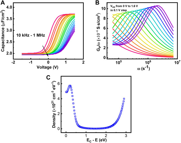
FIGURE 6. Simulated (A) C–V and (B) GP/ω-ω characteristics of the gate stack, considering the impact of bulk traps. (C) Bulk trap state distribution used in the simulation.
In summary, ALD In2O3 transistors and MOS capacitors with 3.5 nm HfO2 as the gate insulator and 3.5 nm In2O3 as the channel semiconductor are fabricated. The interface and bulk traps in this MOS gate stack of ALD In2O3 transistors are systematically studied by using the C–V and conductance method. A low EOT of 0.93 nm is achieved directly from the accumulation capacitance in the C–V curve, indicating a high-quality gate oxide and oxide/semiconductor interface. Defects in bulk In2O3 with the energy level in subgap are confirmed to be responsible for the conductance peak in Gp/ω versus ω curves by TCAD simulations of C–V and G–V characteristics. A high n-type doping of 1 × 10²⁰/cm3 is achieved by C–V measurement, which is further confirmed by the high conductance peak of 7.6 × 10⁻⁶ S∙s/cm2, corresponding to a high subgap DOS of 3.3 × 1020 cm−3 eV−1, which contributes to the high n-type doping and high electron density. The high electron density is because CNL aligns deeply inside the EC, which is speculated to be related to In atoms, thus In-based semiconductors tend to have high electron densities.
The raw data supporting the conclusions of this article will be made available by the authors, without undue reservation.
MS and ZL performed device fabrication. MS and ZL did the electrical measurements. ZW and MS analyzed the electrical data. PY conceived the idea on CNL alignment. ZW conducted TCAD simulations. ZW and MS analyzed the simulation data. ZW, MS, and PY wrote the manuscript.
This work was supported in part by the Semiconductor Research Corporation (SRC) nCore Innovative Materials and Processes for Accelerated Compute Technologies (IMPACT) Center and in part by the Air Force Office of Scientific Research (AFOSR) and SRC/Defense Advanced Research Projects Agency (DARPA) Joint University Microelectronics Program (JUMP) Applications and Systems-driven Center for Energy Efficient integrated Nano Technologies (ASCENT) Center.
The authors declare that the research was conducted in the absence of any commercial or financial relationships that could be construed as a potential conflict of interest.
All claims expressed in this article are solely those of the authors and do not necessarily represent those of their affiliated organizations, or those of the publisher, the editors, and the reviewers. Any product that may be evaluated in this article, or claim that may be made by its manufacturer, is not guaranteed or endorsed by the publisher.
Brammertz, G., Martens, K., Sioncke, S., Delabie, A., Caymax, M., Meuris, M., et al. (2007). Characteristic Trapping Lifetime and Capacitance-Voltage Measurements of GaAs Metal-Oxide-Semiconductor Structures. Appl. Phys. Lett. 91 (13), 133510. doi:10.1063/1.2790787
Chakraborty, W., Grisafe, B., Ye, H., Lightcap, I., Ni, K., and Datta, S. (2020). “BEOL Compatible Dual-Gate Ultra Thin-Body W-Doped Indium-Oxide Transistor with Ion = 370µA/µm, SS = 73mV/dec and Ion/Ioff Ratio > 4x10⁹,” in 2020 IEEE Symposium on VLSI Technology, Honolulu, HI, USA, 16-19 June 2020. TH2.1.
Fujiwara, H., Sato, Y., Saito, N., Ueda, T., and Ikeda, K. (2020). “Surrounding Gate Vertical-Channel FET with a Gate Length of 40 Nm Using BEOL-Compatible High-Thermal-Tolerance In-Al-Zn Oxide Channel,” in Symposium on VLSI Technology (San Francisco, CA: IEEE). TH2.2. doi:10.1109/ted.2020.3021996
Hamberg, I., and Granqvist, C. G. (1986). Evaporated Sn‐doped In2O3films: Basic Optical Properties and Applications to Energy‐efficient Windows. J. Appl. Phys. 60 (11). doi:10.1063/1.337534
Han, K., Kong, Q., Kang, Y., Sun, C., Wang, C., Zhang, J., et al. (2021). “First Demonstration of Oxide Semiconductor Nanowire Transistors: a Novel Digital Etch Technique, IGZO Channel, Nanowire Width Down to ∼20 Nm, and Ion Exceeding 1300 µA/µm,” in 2021 Symposium on VLSI Technology, Kyoto, Japan, 13-19 June 2021. T10-1.
Jankovic, N. (2012). Numerical Simulations of N-type Cdse Poly-TFT Electrical Characteristics with Trap Density Models of Atlas/Silvaco. Microelectronics Reliability 52 (11), 2537–2541. doi:10.1016/j.microrel.2012.03.031
Kamiya, T., and Hosono, H. (2010). Material Characteristics and Applications of Transparent Amorphous Oxide Semiconductors. NPG Asia Mater. 2 (1), 15–22. doi:10.1038/asiamat.2010.5
Kamiya, T., Nomura, K., and Hosono, H. (2010). Present Status of Amorphous In-Ga-Zn-O Thin-Film Transistors. Sci. Techn. Adv. Mater. 11 (4), 044305. doi:10.1088/1468-6996/11/4/044305
Li, S., Gu, C., Li, X., Huang, R., and Wu, Y. (2020). “10-nm Channel Length Indium-Tin-Oxide Transistors with Ion = 1860 μA/μm, Gm = 1050 μS/μm at Vds = 1 V with BEOL Compatibility,” in 2020 IEEE International Electron Devices Meeting (IEDM), San Francisco, CA, USA, 12-18 Dec. 2020, 905–908. doi:10.1109/iedm13553.2020.9371966
Li, S., Tian, M., Gao, Q., Wang, M., Li, T., Hu, Q., et al. (2019). Nanometre-thin Indium Tin Oxide for Advanced High-Performance Electronics. Nat. Mater. 18 (10), 1091–1097. doi:10.1038/s41563-019-0455-8
Matsubayashi, D., Asami, Y., Okazaki, Y., Kurata, M., Sasagawa, S., Okamoto, S., et al. (2015). “20-nm-Node Trench-Gate-Self-Aligned Crystalline In-Ga-Zn-Oxide FET with High Frequency and Low Off-State Current,” in 2015 IEEE International Electron Devices Meeting (IEDM), Washington, DC, USA, 7-9 Dec. 2015, 141–144. doi:10.1109/iedm.2015.7409641
Mönch, W. (1997). Elementary Calculation of the branch-point Energy in the Continuum of Interface-Induced gap States. Appl. Surf. Sci. 117, 380–387.
Nomura, K., Ohta, H., Takagi, A., Kamiya, T., Hirano, M., and Hosono, H. (2004). Room-temperature Fabrication of Transparent Flexible Thin-Film Transistors Using Amorphous Oxide Semiconductors. Nature 432 (7016), 488–492. doi:10.1038/nature03090
Robertson, J., and Clark, S. J. (2011). Limits to Doping in Oxides. Phys. Rev. B 83 (7). doi:10.1103/physrevb.83.075205
Robertson, J., and Falabretti, B. (2006). Band Offsets of High K Gate Oxides on III-V Semiconductors. J. Appl. Phys. 100 (1), 014111. doi:10.1063/1.2213170
Samanta, S., Han, K., Sun, C., Wang, C., Thean, A. V., and Gong, X. (2020). “Amorphous IGZO TFTs Featuring Extremely-Scaled Channel Thickness and 38 Nm Channel Length : Achieving Record High Gm,max of 125 µS/µm at VDS of 1 V and ION of 350 µA/µm,” in 2020 IEEE Symposium on VLSI Technology, Honolulu, HI, USA, 16-19 June 2020. TH2.3.
Schulz, M. (1983). Interface States at the SiO2-Si Interface. in Surface Science 132 (1–3), 422–455. doi:10.1016/b978-0-444-86784-1.50033-x
Si, M., Hu, Y., Lin, Z., Sun, X., Charnas, A., Zheng, D., et al. (2021a). Why In2O3 Can Make 0.7 nm Atomic Layer Thin Transistors. Nano Lett. 21 (1), 500–506. doi:10.1021/acs.nanolett.0c03967
Si, M., Lin, Z., Chen, Z., and Ye, P. D. (2021b). “First Demonstration of Atomic-Layer-Deposited BEOL-Compatible In2O3 3D Fin Transistors and Integrated Circuits: High Mobility of 113 cm2/V∙s, Maximum Drain Current of 2.5 mA/μm and Maximum Voltage Gain of 38 V/V in In2O3 Inverter,” in IEEE Symposium on VLSI Technology (Kyoto, Japan: IEEE), T2–T4.
Si, M., Lin, Z., Charnas, A., and Ye, P. D. (2021c). Scaled Atomic-Layer-Deposited Indium Oxide Nanometer Transistors with Maximum Drain Current Exceeding 2 A/mm at Drain Voltage of 0.7 V. IEEE Electron. Device Lett. 42 (2), 184–187. doi:10.1109/led.2020.3043430
Si, M., Charnas, A., Lin, Z., and Ye, P. D. (2021d). Enhancement-Mode Atomic-Layer-Deposited In2O3 Transistors with Maximum Drain Current of 2.2 A/mm at Drain Voltage of 0.7 V by Low-Temperature Annealing and Stability in Hydrogen Environment. IEEE Trans. Electron. Devices 68 (3), 1075–1080. doi:10.1109/ted.2021.3053229
Si, M., Lin, Z., Chen, Z., Sun, X., Wang, H., and Ye, P. D. (2022). Scaled Indium Oxide Transistors Fabricated Using Atomic Layer Deposition. Nat. Electro. 5 (3), 164–170. doi:10.1038/s41928-022-00718-w
Swallow, J. E. N., Palgrave, R. G., Murgatroyd, P. A. E., Regoutz, A., Lorenz, M., Hassa, A., et al. (2021). Indium Gallium Oxide Alloys: Electronic Structure, Optical Gap, Surface Space Charge, and Chemical Trends within Common-Cation Semiconductors. ACS Appl. Mater. Inter. 13 (2), 2807–2819. doi:10.1021/acsami.0c16021
Wager, J. F., Hoshino, K., Sundholm, E. S., Presley, R. E., Ravichandran, R., Knutson, C. C., et al. (2012). A Framework for Assessing Amorphous Oxide Semiconductor Thin-Film Transistor Passivation. Jnl Soc. Info Display 20 (10), 589–595. doi:10.1002/jsid.120
Keywords: indium oxide, oxide semiconductors, thin-film transistors, atomic layer deposition, interface and bulk traps, conductance method
Citation: Wang Z, Lin Z, Si M and Ye PD (2022) Characterization of Interface and Bulk Traps in Ultrathin Atomic Layer-Deposited Oxide Semiconductor MOS Capacitors With HfO2/In2O3 Gate Stack by C-V and Conductance Method. Front. Mater. 9:850451. doi: 10.3389/fmats.2022.850451
Received: 07 January 2022; Accepted: 07 April 2022;
Published: 04 May 2022.
Edited by:
Kai Ni, Rochester Institute of Technology, United StatesReviewed by:
Pei-Wen Li, National Central University, TaiwanCopyright © 2022 Wang, Lin, Si and Ye. This is an open-access article distributed under the terms of the Creative Commons Attribution License (CC BY). The use, distribution or reproduction in other forums is permitted, provided the original author(s) and the copyright owner(s) are credited and that the original publication in this journal is cited, in accordance with accepted academic practice. No use, distribution or reproduction is permitted which does not comply with these terms.
*Correspondence: Mengwei Si, bWVuZ3dlaS5zaUBzanR1LmVkdS5jbg==; Peide D. Ye, eWVwQHB1cmR1ZS5lZHU=
Disclaimer: All claims expressed in this article are solely those of the authors and do not necessarily represent those of their affiliated organizations, or those of the publisher, the editors and the reviewers. Any product that may be evaluated in this article or claim that may be made by its manufacturer is not guaranteed or endorsed by the publisher.
Research integrity at Frontiers
Learn more about the work of our research integrity team to safeguard the quality of each article we publish.