 Yue Li1Yunxia Zhou2Yanrong Deng1Shiwo Ta3Zhao Yang3Haiou Li1
 Tangyou Sun1
 Yonghe Chen1
 Fabi Zhang1Tao Fu1Peihua Wangyang1
 Jun Zhu2Lizhen Zeng1*
 Xingpeng Liu1*
- 1Guangxi Key Laboratory of Precision Navigation Technology and Application, Guilin University of Electronic Technology, Guilin, China
- 2State Key Laboratory of Electronic Thin Films and Integrated Devices, University of Electronic Science and Technology of China, Chengdu, China
- 3State Key Laboratory of Advanced Materials and Electronic Components, Guangdong Fenghua Advanced Technology Holding Co., Ltd., Zhaoqing, China
The integration of metal oxides and GaAs semiconductors is quite attractive for its potential applications, but interfacial diffusion and lattice mismatch usually cause huge challenges toward achieving high-performance electronic devices. In this article, we reported a thin layer of epitaxial TiO2 (110) on a GaAs (001) substrate with significant compressive strain, lattice distortion, and oxygen vacancies, where the oxygen vacancies proved to be the critical factor to induce the compressive strain and lattice distortion. In this case, the lattice mismatches between this compressed TiO2 (110) and GaAs (001) surface were calculated to be as small as 1.3 and 0.24% along the [110] and [001] orientations of TiO2, respectively. Further, no Ga-oxides or As-oxides were found at the interface, indicating that the TiO2 layer inhibited the diffusion of Ga and As atoms effectively. In summary, TiO2 film can be grown epitaxially on GaAs (001) substrates with non-negligible compressive strain, lattice distortion, oxygen vacancies, and a high-quality interface. This study also provides an approach to integrate different functional oxides on TiO2-buffered GaAs for various GaAs-based electronic devices with higher reliability and performance.
Introduction
Great efforts have been made to integrate epitaxial functional oxides with III-V semiconductor GaAs because of their widely promising applications (Liu et al., 2003; Ueda et al., 2006; Zheng et al., 2006; Wei et al., 2011; Köç et al., 2013; Galatage et al., 2014; Mazet et al., 2015; Lee, 2016; Kornblum et al., 2017; Zhou et al., 2017; Young et al., 2019; Verhulst et al., 2020; Zhou et al., 2020; Dalal et al., 2021). But there still exists some challenges for fabricating functional-oxide/GaAs heterostructures with excellent interfacial quality, such as the large lattice mismatch and interdiffusion of As and Ga atoms. To solve these problems and achieve high-quality interfaces, many studies have attempted to insert a passivation or buffer layer between the functional oxides and GaAs. For instance, Dalapati et al. (2013) prepared a TiAlO alloy dielectric with a passivated GaAs surface by using atomic layer deposition (ALD). Wang et al. (2013) used TaON as an interlayer prior to deposit a high-κ HfTiON gate dielectric, demonstrating that the TaON passivation layer can suppress the formation of interfacial Ga-/As- oxides effectively. Byun et al. (2014) found that a ZnO passivation layer also reduced the extent of diffusion-mediated Ga-O bond formation and near-interface as segregation significantly. In addition, a series of buffer layers have been researched to achieve epitaxial functional oxides on buffered GaAs surfaces. Nashimoto et al. (1992) deposited epitaxial MgO on a GaAs (001) substrate as a buffer layer by pulsed laser deposition. Murphy et al. (2004) investigated the ferroelectric properties of epitaxial BaTiO3 (BTO) deposited on MgO-buffered GaAs, where a large lattice-mismatch between MgO and GaAs led to a poor crystal quality and large leakage current density. Meanwhile, Contreras-Guerrero et al. (2013) investigated the hetero-epitaxy of crystalline perovskite SrTiO3 (STO) on GaAs (001), which had better crystal and interface quality than that which had grown on a MgO buffer layer (Wu et al., 2008; Yang et al., 2013; Meunier et al., 2016). On this basis, Huang et al. deposited epitaxial ZnO, Mn-doped BiFeO3, and BaTiO3 on GaAs (001), yielding good crystal and electrical properties (Huang et al., 2009; Huang et al., 2010; Gao et al., 2013). Louahadj et al. (2013) deposited ferroelectric PZT on STO/GaAs templates by laser molecular beam epitaxy (L-MBE), determining that the STO buffer template can be used to maximally deposit perovskite ferroelectric oxides on GaAs substrates. Although the STO buffer layer presents a relatively smaller lattice mismatch with the GaAs (001) surface, the interdiffusion between GaAs and STO also leads to the formation of Ga-O and As-O bonds, restricting the improvement of electrical properties. Therefore, it still requires further investigation to develop high-quality epitaxial oxide/GaAs heterostructures.
Since the thermodynamic stability of TiO2 is higher than that of STO, the TiO2 buffer layer was considered to inhibit the interfacial diffusion of Ga and As atoms more effectively (Gougousi and Lacis, 2010; Henegar et al., 2016). Based on this theory, we have prepared epitaxial BaTiO3 (110) film on TiO2-buffered GaAs (001) substrates in our previous studies and studied the epitaixial and electrical qualities (Liu et al., 2017). Until now, the oxygen vacancy has been widely studied for its great influence on the physical and chemical properties of oxide films (Lim and Cheong, 2013; Lim and Cheong, 2014; Quah et al., 2020). In this study, we investigated the interface quality between TiO2 and GaAs, including the oxygen vacancies, interfacial diffusion, lattice mismatch, and their relationships.
Experimental Details
The deposition of TiO2 films was carried out by an L-MBE system. A KrF (λ = 248 nm) excimer laser was operated with an energy density of 1.2 J/cm2 at a frequency of 2 Hz. A highly purified TiO2 target was used, and the distance from target to the substrate was kept at 60 mm. Before being loaded into the depositing chamber, the GaAs substrates were ultrasonically cleaned with acetone, alcohol, buffered hydrofluoric acid (pH = 4.5), and acetone again successively. Then, the GaAs substrates were transferred into the depositing chamber and heated to 650°C for 5 min to remove native oxides. The deposition temperature was set at 500°C, and the chamber was evacuated to a base pressure of 1 × 10⁻⁵ Pa during the entire deposition. In this way, TiO2 layers with thicknesses of 2, 10, and 20 nm were deposited on the GaAs (001) substrates. Finally, the fabricated sample is annealed in situ in a 0.1-Pa O2 atmosphere for 10 min. The GaAs wafer was heat-treated at 650°C to decompose and evaporate the native oxides, achieving a clean GaAs surface without Ga-O or As-O bonds. Generally, six kinds of samples were prepared in this study, including as-received GaAs wafer, heat-treated GaAs wafer, TiO2 (2 nm)/GaAs, and TiO2 (20 nm)/GaAs before and after annealing.
The growth process of TiO2 was determined by the typical reflection high energy electron diffraction (RHEED) oscillation technique. Film structure was determined by X-ray diffraction (XRD) with Cu Ka radiation (D1 System, Bede). Film composition was measured by X-ray photoelectron spectroscopy (XPS, AXIS Ultra DLD, Kratos).
Results and Discussion
Crystal Structure of TiO2 Film
Figure 1 shows RHEED patterns during the process of growing TiO2 on the GaAs (001) substrates. Before depositing, the RHEED patterns of the cleaned GaAs surface exhibited clear and bright diffraction spots, as shown in Figure 1A, indicating that the GaAs substrate had been processed well with an atomically flat surface. After 100 pulses of TiO2 deposition (approximately 0.5 nm), the diffraction spots of GaAs nearly disappeared, as shown in Figure 1B. At this moment, the layer was too thin to present the diffraction patterns of TiO2. After depositing 10-nm of TiO2 film, the RHEED pattern along the TiO2 [001] azimuths presented bright diffraction fringes, as shown in Figure 1C, indicating that the TiO2 film grew layer by layer. Figure 1D shows the RHEED pattern of 10-nm TiO2 along the [110] azimuths after rotating the substrate 90° clockwise. Then, the sample was rotated clockwise by another 90°, presenting almost exactly the same diffraction pattern shown in Figure 1C, indicating that the epitaxial TiO2 (110) was of two-fold rotational symmetry. This is why two-fold rotational symmetry BTO (110) film was epitaxially grown on TiO2-buffered GaAs (001) substrate, as we reported previously (Liu et al., 2017). After being annealed in a 0.1-Pa O2 atmosphere for 10 min, the diffraction fringes along the [001] azimuths of the 10-nm TiO2 exhibited bright diffraction spots with a significantly decreased lateral spacing, as shown in Figure 1E, indicating that the lattice constant increased and the compressive strain released. Meanwhile, the diffraction pattern along the [001] azimuths of TiO2 presented the same lateral spacing after annealing, and the diffraction fringes changed into diffraction spots, demonstrating the island-growth mode, as shown in Figure 1F.
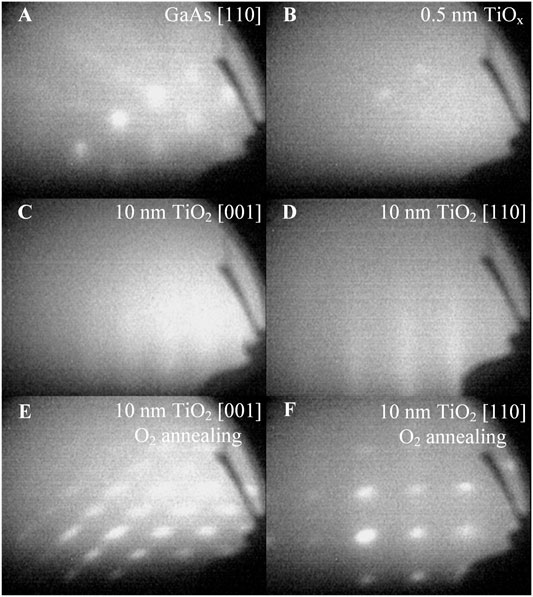
FIGURE 1. RHEED patterns of (A) cleaned GaAs surface along the [110] azimuths; (B) 0.5 nm-TiO2; and (C) 10-nm TiO2 along the [001] azimuths; (D) 10-nm TiO2 along the [110] azimuths; (E) 10-nm TiO2 along the [001] azimuths after annealing; and (F) 10-nm TiO2 along the [110] azimuths after annealing.
XRD was employed to further analyze the effect of the O2 annealing process on the crystal properties of the TiO2 film, as shown in Figure 2A. The as-deposited TiO2 film presented very weak diffraction peaks of the rutile TiO2 (110) phase, which can be ascribed to lattice distortion. After annealing in O2, diffraction peaks of the rutile TiO2 (110) and (220) planes were clearly observed, indicating the good crystalline quality of rutile TiO2 (110) film due to the release of compressive strain. In order to explain the in-plane epitaxial relationship between the TiO2 (110) film and GaAs (001) substrate visually, a detailed lattice-matching schematic diagram was plotted, as shown in Figure 2B. As it is known, rutile-phase TiO2 is tetragonal with a = 0.4593 nm and c = 0.2959 nm, and the lateral spacing of a RHEED pattern is inversely proportional to the relevant lattice constant. On this basis, the theoretical lattice constant of standard TiO2 along the [110] azimuths was calculated as 0.6494 nm, which was used as a standard to determine the lattice constants of compressed TiO2, corresponding to a lateral spacing of 181 pixels in Figure 1E. The lateral spacing in Figures 1C,D was measured as 290 and 391 pixels, so the corresponding lattice constants of compressed TiO2 was estimated as 0.4050 and 0.3005 nm along the [110] and [001] directions, respectively. In this case, the in-plane epitaxial relationship of the TiO2/GaAs heterostructure was plotted, as shown in Figure 2B. Obviously, two compressed TiO2 cells matched well with 0.75 GaAs cells along the TiO2 [001] and GaAs [1-10] directions, and the calculated lattice mismatch was as small as 0.24%. Further, two compressed TiO2 cells matched with one GaAs cell along the TiO2 [110] and GaAs [110] directions, with a calculated lattice-mismatch value of 1.30%. In contrast, the lattice mismatches between standard TiO2 and the GaAs substrate were calculated to be 1.29 and 18.76% along the TiO2 [001] and TiO2 [110] directions, respectively. Thus, these results reveal the epitaxial mechanism of TiO2 (110) on GaAs (001), in which the TiO2 (110) film deposited on the GaAs (001) surface with non-negligible lattice distortion and compressive strain due to their lattice mismatch.
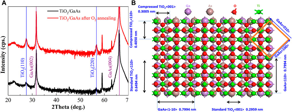
FIGURE 2. (A) XRD 2θ scans of the TiO2/GaAs heterostructure with and without in-situ annealing in O2; (B) In-plane epitaxial relationship between GaAs (001) and TiO2 (110) with compressive strain.
Chemical Composition and Valence
In order to evaluate the chemical composition of TiO2 with compressive strain, XPS depth profiles of Ti 2p and O 1s were recorded under a 20-nm thickness of TiO2 via Ar-ion beam sputtering technology, as shown in Figures 3A,B. XPS spectra measured at different depths were significantly inconsistent, and complex low-oxidation states of Ti cations were obtained in depth profiles at thicknesses of 3–15 nm. These XPS results showed that the as-deposited, compressed TiO2 films can be easily oxidized to form a thin and standard TiO2 layer at the surface when exposed to air. All these XPS spectral were calibrated by C peak at 284.6 eV, and the Ti 2p peaks can be divided for six peaks at 458.3 eV (Ti4+ 2p3), 456.5 eV (Ti3+ 2p3), 454.7 eV (Ti2+ 2p3), 464.1 eV (Ti4+ 2p1), 462.4 eV (Ti3+ 2p1), and 460.5 eV (Ti2+ 2p1). Similarly, the O 1s peaks can be divided for two peaks at 532.8 eV (oxygen vacancies) and 531.3 eV (O 1s). In this way, the total area of Ti 2p or O 1s peaks were calculated by adding the area of all divided peaks. According to the area ratio of Ti 2p, O 1s peaks and their sensitivity factors (Gouttebaron et al., 2000; Guillot et al., 2002), the contents ratios of Ti and O atoms can be calculated as 40,065.57:75,730.88, 51,237.13:96,420.32, 58,893.03:97,903.33, 57,899.32:93,273.84, 59,279.73:95,497.64, and 60,600.82:97,625.87. On this basis, the contents of Ti ions were determined as 34.65, 34.73, 37.62, 38.30, 38.31, and 38.31% at depths of 0, 3, 6, 9, 12, and 15 nm, respectively, as shown in Figure 3C. These results indicate that the compressed TiO2 film had a stable chemical composition at depths greater than 9 nm. In addition, the effect of the in-situ O2 annealing process was also investigated, as shown in Figures 3D,E. XPS spectra of the As-deposited. TiO2 exhibited peaks corresponding to the low-valence-state of Ti ions and oxygen vacancies. Nevertheless, these XPS peaks disappeared after annealing in the O2 atmosphere for 20 min, indicating that oxygen vacancies can be repaired well by this O2 annealing process. Taking all the above crystal and XPS observations together, it can be concluded that oxygen defects were a key reason for the formation of epitaxial TiO2 film with compressive strain and lattice distortion.
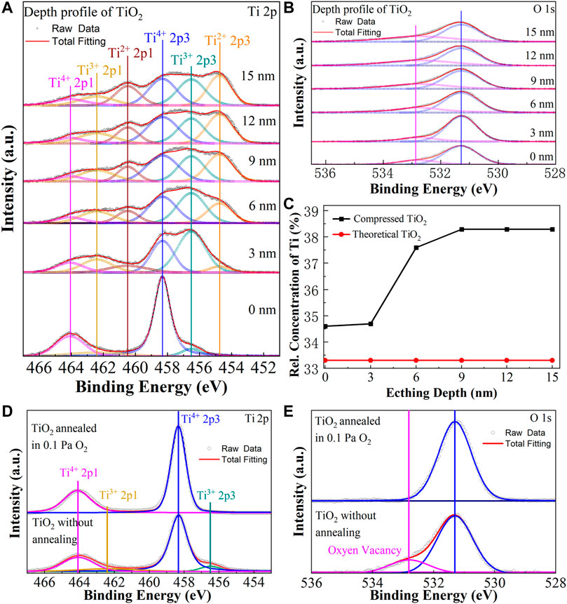
FIGURE 3. Ex-situ XPS spectra of (A) Ti 2p and (B) O 1s at different depths. (C) Relative concentration of Ti atoms as a function of etching depth. (D) Ex-situ XPS spectra of Ti 2p with and without in-situ annealing in 0.1-Pa O2. (E) Ex-situ XPS spectra of O 1s with and without in-situ annealing in 0.1-Pa O2.
To provide further insight into the effect of TiO2 film on inhibiting interfacial diffusion, 2-nm-thick TiO2 films were deposited in high vacuum to fabricate TiO2/GaAs, and the interfacial quality was determined by XPS. In addition, the original GaAs surface and the GaAs surface without native oxides were also employed for comparison. As shown in Figure 4A, the As-Ga, As-As, and As-O bonds were detected at 40.8, 41.5, and 44.3 eV, respectively, where the existence of the As-O bond was ascribed to the native oxides at the surface of GaAs. Meanwhile, Figure 4B shows the ex-situ XPS As 3d spectrum of the GaAs substrate after heat-treatment at 650°C in high vacuum. An As-O peak can be barely observed, indicating that As-oxides were completely removed. Figures 4C,D show As 3d spectra of TiO2(2 nm)/GaAs samples. Similarly, As-O peaks cannot be detected in these two spectra whether the annealing process was employed or not, indicating that TiO2 film can effectively inhibit the diffusion of As atoms and the formation of As-oxides.
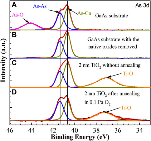
FIGURE 4. (A) XPS core-level spectra of As 3d from (A) as-received GaAs wafer; (B) cleaned GaAs wafer without native oxides; (C) TiO2 (2 nm)/GaAs heterostructure without O2 annealing; and (D) TiO2 (2 nm)/GaAs heterostructure after O2 annealing.
The XPS spectra of Ga 3d for the different samples were also provided as shown in Figure 5. Figure 5A shows that obvious Ga-O bonds were detected at the surface of the as-received GaAs wafer, indicating the presence of Ga2O, GaO, and Ga2O3. Meanwhile, the intensities of the Ga-O peaks decreased significantly after heat-treatment, as shown in Figure 5B, indicating that the native Ga-oxides can be mostly removed by heat-treatment. Combining the barely observed Ga-O peaks in Figures 5C,D, it can be inferred that the Ga-O bonds in Figure 5B were the result of oxidation via air, prior to carrying out XPS measurements. In addition, the absence of Ga-O bonds for the as-deposited TiO2 (2 nm)/GaAs samples demonstrated the effective inhibition of TiO2 toward the diffusion of Ga atoms, which was attributed to the formation of Ga-Ti bonds. After annealing in an O2 atmosphere, Ga-O peaks appears again, but no Ga-Ti peaks were observed, showing that the existence of Ga-Ti bonds may be the critical reason for suppressing the formation of Ga-oxides. In conclusion, a TiO2 passivation layer without O2 annealing can suppress the diffusion of Ga and As atoms and inhibit the formation of As-oxides and Ga-oxides at the interface of the TiO2/GaAs heterostructure successfully.
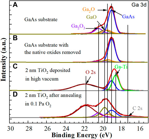
FIGURE 5. XPS core-level spectra of Ga 3d from (A) GaAs wafer; (B) GaAs substrate with native oxides removed; (C) TiO2 (2 nm)/GaAs heterostructure without annealing; and (D) TiO2 (2 nm)/GaAs heterostructure with annealing in 0.1-Pa O2.
Conclusion
In this article, we demonstrated the epitaxial growth mechanism of TiO2 (110) films on GaAs (001) substrates with large lattice distortion and compressive strain. The lattice mismatches are calculated to be only 1.3 and 0.24%, along the TiO2 [110] and [001] orientations, respectively. Strictly speaking, non-negligible oxygen vacancies are proven to exist in this compressed TiO2 film and the chemical formula should be determined as Ti0.383O0.617. These oxygen vacancies can be healed by annealing in O2 atmosphere, which results in the release of compressive strain. Besides, XPS results show that the formation of Ga-oxides and As-oxides can be effectively inhibited by suppressing the interfacial diffusion of Ga and As atoms at the TiO2/GaAs interface. In summary, the reason for the epitaixal growth of TiO2 on GaAs (001) substrate can be concluded as the combined action of oxygen vacancies and lattice distortion. These findings provide a new method for integrating functional oxides on GaAs substrates with high-performance interfacial quality.
Data Availability Statement
The original contributions presented in the study are included in the article/Supplementary Material, further inquiries can be directed to the corresponding authors.
Author Contributions
YL and XL designed the experiments. YL and LZ performed the experiments. YD, ST, TS, YC, FZ, TF and PW analyzed the data. YZ and JZ contributed the materials. YL and XL wrote the manuscript. YD, ST, ZY and HL contributed to the modification and suggestion in this manuscript.
Funding
Project supported by Guangxi Science and Technology Planning Project (Grant Nos. AD19245066, AA19254015, AD21220150 and AD18281037), China Postdoctoral Science Foundation (Grant No. 2020M683626XB), National Nature Science Foundation of China (Grant Nos. 61874036, 62174041 and 62041403), Natural Science Foundation of Guangxi Province (Grant No. 2018GXNSFAA138025), Guangxi Innovation Research Team Project (Grant No. 2018GXNSFGA281004), Opening Foundation of the State Key Laboratory of Advanced Materials and Electronic Components (Grant No. FHR-JS-201909007), Guangxi Key Laboratory of Precision Navigation Technology and Application (Grant Nos. DH2020013 and DH201906). GUET Excellent Graduate Thesis (Grant No. YXYJRX01), State Key Laboratory of ASIC & System (Grant No. KVH1233021), Basic Ability Improvement Project of Young and Middle-Aged Teachers in Guangxi Universities, speech recognition application research based on intelligent artificial swarm technology (Grant No. 2019KY0212).
Conflict of Interest
ST and ZY were employed by Guangdong Fenghua Advanced Technology Holding Co., Ltd.
The remaining authors declare that the research was conducted in the absence of any commercial or financial relationships that could be construed as a potential conflict of interest.
Publisher’s Note
All claims expressed in this article are solely those of the authors and do not necessarily represent those of their affiliated organizations, or those of the publisher, the editors, and the reviewers. Any product that may be evaluated in this article, or claim that may be made by its manufacturer, is not guaranteed or endorsed by the publisher.
References
Byun, Y.-C., Choi, S., An, Y., McIntyre, P. C., and Kim, H. (2014). Tailoring the Interface Quality between HfO2 and GaAs via In Situ ZnO Passivation Using Atomic Layer Deposition. ACS Appl. Mater. Inter. 6, 10482–10488. doi:10.1021/am502048d
Contreras-Guerrero, R., Edirisooriya, M., Noriega, O. C., and Droopad, R. (2013). Interface Properties of MBE Grown Epitaxial Oxides on GaAs. J. Cryst. Growth 378, 238–242. doi:10.1016/j.jcrysgro.2012.12.131
Dalal, A., Dhar Dwivedi, S. M. M., Ghosh, C., Lahiri, R., Henini, M., and Mondal, A. (2021). Mg:TiO2 alloy Thin Films Based MOS Capacitors Grown on GaAs Substrates. J. Alloys Comp. 868, 159178. doi:10.1016/j.jallcom.2021.159178
Dalapati, G. K., Chia, C. K., Tan, C. C., Tan, H. R., Chiam, S. Y., Dong, J. R., et al. (2013). Surface Passivation and Interface Properties of Bulk GaAs and Epitaxial-GaAs/Ge Using Atomic Layer Deposited TiAlO alloy Dielectric. ACS Appl. Mater. Inter. 5, 949–957. doi:10.1021/am302537b
Galatage, R. V., Zhernokletov, D. M., Dong, H., Brennan, B., Hinkle, C. L., Wallace, R. M., et al. (2014). Accumulation Capacitance Frequency Dispersion of III-V Metal-Insulator-Semiconductor Devices Due to Disorder Induced gap States. J. Appl. Phys. 116, 014504. doi:10.1063/1.4886715
Gao, G. Y., Yang, Z. B., Huang, W., Zeng, H. Z., Wang, Y., Chan, H. L. W., et al. (2013). Heteroepitaxial Growth and Multiferroic Properties of Mn-Doped BiFeO3 Films on SrTiO3 Buffered III-V Semiconductor GaAs. J. Appl. Phys. 114, 094106. doi:10.1063/1.4820579
Gougousi, T., and Lacis, J. W. (2010). Native Oxide Consumption during the Atomic Layer Deposition of TiO2 Films on GaAs (100) Surfaces. Thin Solid Films 518, 2006–2009. doi:10.1016/j.tsf.2009.08.028
Gouttebaron, R., Cornelissen, D., Snyders, R., Dauchot, J. P., Wautelet, M., and Hecq, M. (2000). XPS Study of TiOx Thin Films Prepared by d.C. Magnetron Sputtering in Ar-O2 Gas Mixtures. Surf. Interf. Anal. 30, 527–530. doi:10.1002/1096-9918(200008)30:1<527::AID-SIA834>3.0.CO;2-Z
Guillot, J., Jouaiti, A., Imhoff, L., Domenichini, B., Heintz, O., Zerkout, S., et al. (2002). Nitrogen Plasma Pressure Influence on the Composition of TiNxOy Sputtered Films. Surf. Interf. Anal. 33, 577–582. doi:10.1002/sia.1423
Henegar, A. J., Cook, A. J., Dang, P., and Gougousi, T. (2016). Native Oxide Transport and Removal during Atomic Layer Deposition of TiO2 Films on GaAs(100) Surfaces. ACS Appl. Mater. Inter. 8, 1667–1675. doi:10.1021/acsami.5b08998
Huang, W., Dai, J. Y., and Hao, J. H. (2010). Structural and Resistance Switching Properties of ZnO/SrTiO3/GaAs Heterostructure Grown by Laser Molecular Beam Epitaxy. Appl. Phys. Lett. 97, 162905. doi:10.1063/1.3505136
Huang, W., Wu, Z. P., and Hao, J. H. (2009). Electrical Properties of Ferroelectric BaTiO3 Thin Film on SrTiO3 Buffered GaAs by Laser Molecular Beam Epitaxy. Appl. Phys. Lett. 94, 032905. doi:10.1063/1.3075955
Kornblum, L., Fenning, D. P., Faucher, J., Hwang, J., Boni, A., Han, M. G., et al. (2017). Solar Hydrogen Production Using Epitaxial SrTiO3 on a GaAs Photovoltaic. Energy Environ. Sci. 10, 377–382. doi:10.1039/c6ee03170f
Köç, P., Tekmen, S., Baltakesmez, A., Tüzemen, S., Meral, K., and Onganer, Y. (2013). Stimulated Electroluminescence Emission from N-ZnO/p-GaAs:Zn Heterojunctions Fabricated by Electro-Deposition. AIP Adv. 3, 122107. doi:10.1063/1.4842635
Lee, S. W. (2016). Two-Dimensional Electron Gas at SrTiO3-Based Oxide Heterostructures via Atomic Layer Deposition. J. Nanomater. 2016, 1–9. doi:10.1155/2016/1671390
Lim, W. F., and Cheong, K. Y. (2013). Effects of post-deposition Annealing Temperature on Metal-Organic Decomposed Lanthanum Cerium Oxide Film as Metal Reactive Oxide Layer on 4H-SiC. Mater. Chem. Phys. 140, 622–633. doi:10.1016/j.matchemphys.2013.04.016
Lim, W. F., and Cheong, K. Y. (2014). Oxygen Vacancy Formation and Annihilation in Lanthanum Cerium Oxide as a Metal Reactive Oxide on 4H-Silicon Carbide. Phys. Chem. Chem. Phys. 16, 7015–7022. doi:10.1039/c3cp55214d
Liu, X. H., Liu, Z. G., Wang, Y. P., Zhu, T., and Liu, J. M. (2003). Characteristics of SrBi 2 Ta 2 O 9 Ferroelectric Films on GaAs with a TiO 2 Buffer Layer. Appl. Phys. A: Mater. Sci. Process. 76, 197–199. doi:10.1007/s003390201417
Liu, X., Zhu, J., and Wu, Z. (2017). Epitaxial Deposition of BaTiO 3 on TiO 2 Buffered GaAs(001) Substrate. Thin Solid Films 641, 38–42. doi:10.1016/j.tsf.2017.01.067
Louahadj, L., Le Bourdais, D., Largeau, L., Agnus, G., Mazet, L., Bachelet, R., et al. (2013). Ferroelectric Pb(Zr,Ti)O3 Epitaxial Layers on GaAs. Appl. Phys. Lett. 103, 212901. doi:10.1063/1.4831738
Mazet, L., Yang, S. M., Kalinin, S. V., Schamm-Chardon, S., and Dubourdieu, C. (2015). A Review of Molecular Beam Epitaxy of Ferroelectric BaTiO3films on Si, Ge and GaAs Substrates and Their Applications. Sci. Techn. Adv. Mater. 16, 036005. doi:10.1088/1468-6996/16/3/036005
Meunier, B., Bachelet, R., Grenet, G., Botella, C., Regreny, P., Largeau, L., et al. (2016). The Role of Titanium at the SrTiO 3/GaAs Epitaxial Interface. J. Cryst. Growth 433, 139–142. doi:10.1016/j.jcrysgro.2015.10.013
Murphy, T. E., Chen, D., and Phillips, J. D. (2004). Electronic Properties of Ferroelectric BaTiO3∕MgO Capacitors on GaAs. Appl. Phys. Lett. 85, 3208–3210. doi:10.1063/1.1804237
Nashimoto, K., Fork, D. K., and Geballe, T. H. (1992). Epitaxial Growth of MgO on GaAs(001) for Growing Epitaxial BaTiO3thin Films by Pulsed Laser Deposition. Appl. Phys. Lett. 60, 1199–1201. doi:10.1063/1.107404
Quah, H. J., Hassan, Z., and Lim, W. F. (2020). Preparation and Characterisation of Aluminium Zirconium Oxide for Metal‐oxide‐semiconductor Capacitor. Int. J. Energ. Res. 44, 10562–10575. doi:10.1002/er.5693
Ueda, T., Noma, A., and Ueda, D. (2006). GaAs MMIC Chip-Sets for mobile Communication Systems with On-Chip Ferroelectric Capacitors. Integrated Ferroelectrics 7, 45–60. doi:10.1080/10584589508220220
Verhulst, A. S., Saeidi, A., Stolichnov, I., Alian, A., Iwai, H., Collaert, N., et al. (2020). Experimental Details of a Steep-Slope Ferroelectric InGaAs Tunnel-FET with High-Quality PZT and Modeling Insights in the Transient Polarization. IEEE Trans. Electron. Devices 67, 377–382. doi:10.1109/ted.2019.2954585
Wang, L. S., Xu, J. P., Zhu, S. Y., Huang, Y., and Lai, P. T. (2013). Improved Interfacial and Electrical Properties of GaAs Metal-Oxide-Semiconductor Capacitors with HfTiON as Gate Dielectric and TaON as Passivation Interlayer. Appl. Phys. Lett. 103, 092901. doi:10.1063/1.4818000
Wei, X. H., Huang, W., Yang, Z. B., and Hao, J. H. (2011). Interfacial and Rectifying Characteristic of Epitaxial SrTiO3-δ/GaAs P-N Junctions. Scripta Materialia 65, 323–326. doi:10.1016/j.scriptamat.2011.04.035
Wu, Z. P., Huang, W., Wong, K. H., and Hao, J. H. (2008). Structural and Dielectric Properties of Epitaxial SrTiO3 Films Grown Directly on GaAs Substrates by Laser Molecular Beam Epitaxy. J. Appl. Phys. 104, 054103. doi:10.1063/1.2974796
Yang, Z., Huang, W., and Hao, J. (2013). Determination of Band Alignment of Pulsed-Laser-Deposited Perovskite Titanate/III-V Semiconductor Heterostructure Using X-ray and Ultraviolet Photoelectron Spectroscopy. Appl. Phys. Lett. 103, 031919. doi:10.1063/1.4816356
Young, L. B., Cheng, C.-K., Lin, K.-Y., Lin, Y.-H., Wan, H.-W., Cai, R.-F., et al. (2019). Epitaxy of High-Quality Single-Crystal Hexagonal Perovskite YAlO3 on GaAs(111)A Using Laminated Atomic Layer Deposition. Cryst. Growth Des. 19, 2030–2036. doi:10.1021/acs.cgd.8b01375
Zheng, L., Zhu, J., Zhang, Y., Jiang, S. W., Li, Y. R., HuaWei, X., et al. (2006). Characterization of Bicrystalline Epitaxial LaNiO3 Films Fabricated on MgO (100) Substrates by Pulsed Laser Deposition. Appl. Surf. Sci. 252, 3609–3615. doi:10.1016/j.apsusc.2005.05.044
Zhou, Y., Liu, X., and Zhu, J. (2020). Controlled High-Quality Interface of a Ti2.5O3(0 1 0)/GaAs(0 0 1) Heterostructure Enabled by Minimized Lattice Mismatch and Suppressed Ion Diffusion. J. Colloid Interf. Sci. 560, 769–776. doi:10.1016/j.jcis.2019.10.041
Keywords: epitaxial, RHEED, TiO2, compressive strain, GaAs
Citation: Li Y, Zhou Y, Deng Y, Ta S, Yang Z, Li H, Sun T, Chen Y, Zhang F, Fu T, Wangyang P, Zhu J, Zeng L and Liu X (2022) Formation and Effect of Deposited Thin TiO2 Layer With Compressive Strain and Oxygen Vacancies on GaAs (001) Substrate. Front. Mater. 9:846428. doi: 10.3389/fmats.2022.846428
Received: 31 December 2021; Accepted: 16 March 2022;
Published: 27 April 2022.
Edited by:
Jinn P. Chu, National Taiwan University of Science and Technology, TaiwanReviewed by:
Way Foong Lim, Universiti Sains Malaysia (USM), MalaysiaManuel Pereira Dos Santos, University of Evora, Portugal
Pangpang Wang, Kyushu University, Japan
Copyright © 2022 Li, Zhou, Deng, Ta, Yang, Li, Sun, Chen, Zhang, Fu, Wangyang, Zhu, Zeng and Liu. This is an open-access article distributed under the terms of the Creative Commons Attribution License (CC BY). The use, distribution or reproduction in other forums is permitted, provided the original author(s) and the copyright owner(s) are credited and that the original publication in this journal is cited, in accordance with accepted academic practice. No use, distribution or reproduction is permitted which does not comply with these terms.
*Correspondence: Xingpeng Liu, dGFkeWxpdUBndWV0LmVkdS5jbg==; Lizhen Zeng, NjE3MzUwNTM1QHFxLmNvbQ==