 Chuanzhe Ma1
 Xinchang Wang
 Bingfeng Fan
- 1School of Electronics and Information Technology, Sun Yat-sen University, Guangzhou, China
- 2School of Physics and Optoelectronic Engineering, Foshan University, Foshan, China
- 3Guangdong-Hong Kong-Macao Joint Laboratory for Intelligent Micro-Nano Optoelectronic Technology, Foshan University, Foshan, China
- 4State Key Laboratory of Optoelectronics Materials and Technologies, Sun Yat-sen University, Guangzhou, China
In this letter, we describe the design and fabrication of high-power AlGaN-based ultraviolet (UV) flip-chip high-voltage light-emitting diodes (LEDs) operating at 368 nm with an epitaxial indium tin oxide (ITO)/Al reflecting mirror and symmetry electrode layout. Metal-organic chemical vapor deposition (MOCVD) was used to grow an ITO thin film as a transparent electrode on the LED surface. At 365 nm, epitaxial ITO thin films exhibited a transmittance of up to 93.6%. Additionally, the epitaxial ITO/Al reflective mirror has a reflectance of 81.2% at 365-nm. To investigate the electrical characteristics, four types of HV-LED micro-cells were constructed with varying n-type mesa structures and p-type interconnect electrodes. We demonstrated a forward voltage (Vf) of 7.86 V at 350 mA with a 2 × 2 mico-cells high-voltage ultraviolet 368-nm flip-chip LED after optimising electrode structure and device process.
1 Introduction
AlGaN-based ultraviolet (UV) LEDs have gained increasing attention due to the growing demand for UV curing, solid-state lighting, medical sterilization, laser security, among other applications (Khan et al., 2008). UV LEDs are rapidly displacing conventional ultraviolet sources, such as high-pressure mercury vapour lamps, due to their narrow spectrum, low operating voltage, high energy efficiency, long lifetime, low power consumption, small size, and environmental friendliness (Kneissl et al., 2011; Muramoto et al., 2014). Referring to specific wavelengths in high-pressure mercury vapour lamps, such as i-line (365 nm), h-line (405 nm), and g-line (436 nm), GaN-based LEDs also have the highest emission efficiency in the h- and g-line spectral regions. However, the efficiency of 365 nm UV LEDs in the i-line spectral region is still too low for many applications due to the poor crystal quality and low hole density of AlGaN (Khan et al., 2008; Shatalov et al., 2012). Numerous strategies for increasing the luminous efficiency of ultraviolet LEDs have been proposed, including improving the internal quantum efficiency (IQE), increasing p-doping efficiency, improving carrier transport, increasing light extraction efficiency, and decreasing self-heating (Mukai and Nakamura, 1999; Svensk et al., 2008; Shatalov et al., 2012; Lin et al., 2014; Liu et al., 2016).
Increased light output per unit area, photoelectric conversion efficiency, and efficiency droop effect have all been demonstrated using high voltage LEDs (Wang et al., 2011; Tien et al., 2017). External quantum efficiency of 365 nm UV LED chip is currently low (Khan et al., 2008). Enhancing the power of ultraviolet LEDs with a high voltage LED chip is an effective technique to do it (Tien et al., 2017). Now, high voltage LEDs documented in the literature are generated by connecting standard micro-cell LEDs. The heat issues that the high voltage LED creates are rather serious. Thermal issues must be addressed using flip-chip arrangement (Wu et al., 2017a; Wu et al., 2017b; Zhang et al., 2018). There are, however, two challenges associated with producing 365-nm high-voltage flip-chip LEDs. The main challenge of developing high-efficiency UV LED chip is to realize the reflective electrode with high reflectivity, good contact and stable operation in 365 nm band. There have been numerous reports on various types of ultraviolet mirrors, including metal mirrors, distributed Bragg reflectors (DBRs), omnidirectional reflectors (ODRs), and tin-doped indium oxide (ITO)/Al reflectors (Lobo et al., 2010; Lin et al., 2010; Takehara et al., 2012; Choi et al., 2013; Nakashima et al., 2013; Chong and Lau, 2014; Kim et al., 2014; Kuo et al., 2015). However, the UV Mirrors reported in the literature still had the problems of low reflectivity in 365 nm band, poor electrical performance in contact with p-AlGaN and bad heat dissipation performance. Therefore, excellent UV mirror is necessary for high-power LED. ITO/Al is the most often reported and used UV reflective electrode material among them. The ITO materials described in the literature are typically produced via sputtering and have a transmittance of less than 80% in the 365 nm band. Dr. Chen observed that by enhancing the quality of the crystal material, the ITO material generated by MOCVD process has a 95% transmittance in the ultraviolet 365 nm band (Chen et al., 2017). We applied this material to the LED reflector in this investigation. Another issue to resolve is the interconnection between the flip-chip high-voltage LED chip and the substrate. Traditionally, connectivity is made via the substrate. The positive and negative poles of each chip on the high-voltage LED chip must be aligned with the positive and negative poles on the substrate when flip-chip welding. Otherwise, it is easy to cause short circuits in the devices because of the presence of a poor solder joint. Due to the fact that virtual or weak welding will influence the entire high-voltage chip, this process is complex and yields are low. The manufacturing of UV 368-nm AlGaN-based flip-chip high-voltage LEDs in this work utilized an epitaxial indium tin oxide/Al reflecting mirror and symmetry electrode configuration. To investigate the performance, various types of HV-LED microcells with an n-type mesa structure and a p-type connecting electrode were developed.
2 Experiments
In this work, MOCVD was used to grow AlGaN-based ultraviolet LED epitaxial structures on a 2-inch c-plane patterned sapphire substrate with a thickness of 430-μm. The LED structure used in this study was composed of a 20-nm AlGaN buffer layer grown at 560°C, a 4-μm thick unintentionally doped AlGaN template layer, a 2-μm thick Si-doped n-AlGaN layer grown at 1,100°C, a 150-nm thick strain compensated AlGaInN/AlGaN superlattice layer, a 250-nm thick 9-pair AlGaInN/AlGaN multiple quantum well grown at 800°C, a 40-nm n-AlGaN electron blocking layer grown at 900°C, a 100-nm thick Mg-doped p-AlGaN grown at 950°C, and a 3-nm thick p+-GaN as contact layer. Trimethylaluminum (TMAl), trimethylindium (TMIn), trimethylgallium (TMGa), and ammonia (NH3) were used as the Al, In, Ga, and N precursors, respectively. Bis(cyclopentadienyl)magnesium (Cp2Mg) and silane (SiH4) were used as the p-type and n-type doping sources, respectively. Hydrogen (H2) and nitrogen (N2) were used as carrier gas. Thermal annealing was performed at 700°C for 20 min under a N2 ambient to activate the Mg dopant. Then, using a modified Veeco Emcore400 MOCVD system, a 50-nm-thick ITO film was grown as a transparent conductive layer on the surface of the LED epitaxial layer. The following section describes the detailed growth conditions of ITO. Trimethylindium (TMIn), tetrakis-dimethylamino Tin (TDMASn), and oxygen were used as precursors for the In, Sn, and O precursors, respectively, and Argon (Ar) as the carrier gas. 500°C and 12.5 Torr were used as the growth temperatures and chamber pressures, respectively. The ITO was deposited with a Sn flow rate of 250 sccm, corresponding to a maximum Sn/In mole flow ratio of 1:5. The structure of our AlGaN-Based flip-chip ultraviolet high-voltage light-emitting diodes with epitaxial ITO/Al reflective mirror and symmetry electrode arrangement was shown in Figure 1H, and the process flow of the high-voltage LED chip was as follows. First, the ITO layer was partially removed by HCl and HNO3 solution, 10:1, followed by inductively coupled plasma (ICP) etching to form the mesa structure, and the 1.35-μm depth of the AlGaN layers was then etched away to reveal the n-AlGaN layer. Subsequently, 6-μm isolation trench was obtained by combining photolithography and subsequent ICP deep etching process based on BCl3/Cl2 plasmas, as shown in Figure 1B. Then, the reflective metal layers Cr/Al/Ni/Au (0.3/250/20/60 nm) was deposited on the ITO surface to form a good ohmic contact with ITO, as well as a UV high reflective interface, as shown in Figure 1C. Next, a 1-μm-thick first SiO2 passivation layer was deposited by using plasma-enhanced chemical vapor deposition (PECVD) method to prevent short circuits among LED cells, as shown in Figure 1D. After etching the SiO2 to expose a portion of the area n-pad and reflective layer, a Cr/Al/Ni/Au (5/200/20/50 nm) structure was deposited as n-pad and p-pad electrode materials, as shown in Figure 1E. Then, as shown in Figure 1F, a 1-μm-thick second SiO2 was deposited on the above structure as the insulation layer by plasma-enhanced chemical vapor deposition (PECVD) with a 300°C deposition temperature and 10 W deposition power, respectively. The insulation layer was partially removed by 7:1 buffered oxide agent (BOE) to expose a portion of the area n-fingers and the reflective layer. Then the symmetry electrode metal layers Cr/Al/Ni/Au (5/250/50/60 nm), n-pad and p-pad, was deposited by electron beam evaporation and was thickened by electroplating 1-μm gold layer, as shown in Figure 1G. The n-pad and p-pad are respectively connected to n-fingers and reflective layers through the holes in the insulating layer. Not only does the electroplated gold layer reinforce the electrical connection, it also enhances heat dissipation performance.
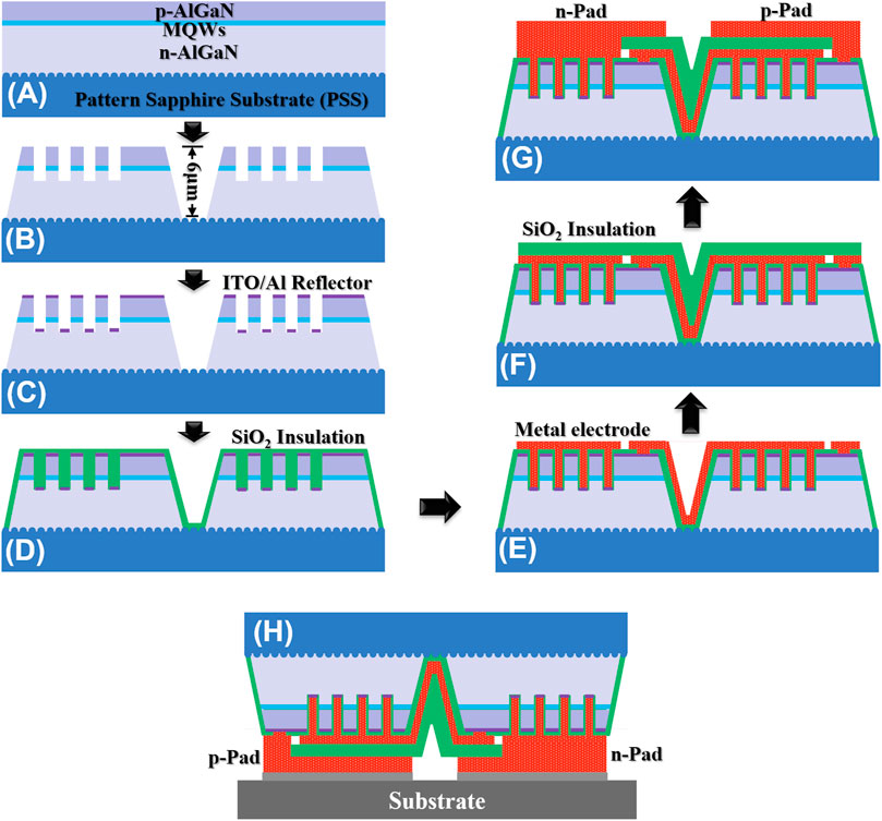
FIGURE 1. (color online) The process flow of the flip-chip UV HV-LED with a reflective metal layer and the symmetric electrode. (A) ITO epitaxy. (B) n-AlGaN etching and deep isolation trench etching. (C) Reflector mirrors evaporate. (D) First SiO2 insulation. (E) Electrode deposition. (F) Second SiO2 insulation. (G) n-pad and p-pad. (H) Cross-sectional view.
Four different types of HV-LED micro-cells with varying n-type mesa structure and p-type interconnect electrode were constructed to investigate performance. These are labelled A1 (n-dots mesa), A2 (n-dots mesa and interdigitated p-finger), B1 (n-finger mesa), B2 (n-finger mesa and interdigitated p-finger), respectively. The micro-cells have the same dimensions of 1140 μm × 1140 μm, and the active emission areas for structures A1, A2, B1, B2 were 1.19, 1.19, 1.15, and 1.15 mm2, respectively. The injection current-voltage (I-V) characteristics of the UV LEDs without packaging were measured using an Agilent B1500A semiconductor device analyzer and a FitTech IPT6000 chip wafer probing and testing system. The transmittance of the ITO thin films and the reflectance of the ITO/Al (50/250 nm) layers were determined using a Shimadzu UV-2550 spectrophotometer.
3 Results and Discussion
Deep isolation trenches separate high voltage LEDs into electrically isolated micro-cells, which is a critical and necessary process in the fabrication of HV-LED device. S. Zhou et al. study the effect of profile and size of isolation trench on the optical and electrical performance of GaN-based high-voltage LEDs (Zhou et al., 2016). In our study, we use the properties of photoresist which can form a smooth sidewall with a certain inclination angle after the post-bake process to obtain tapered sidewalls with different angles. EXP-1520T photoresist with a thickness of 8 μm was used, and the etching ratio of AlGaN to photoresist is 1:1 under the ICP etching conditions of 200 W etching power, 80 W bias power, and flow rate of Cl2, BCl3, N2 are 30, 5, and 10 sccm, respectively. Figure 2 shows the SEM of tapered sidewalls after etching by ICP etching with an inclination of 42°, 53°, and 65° to the horizontal. The tapered sidewalls of 65° show smaller interconnect resistance, larger luminous region, but poor step coverage, while the tapered sidewalls of 42° are the opposite. Therefore, tapered sidewalls of 53° are more suitable for application in our device structure. The device test results also prove this point. Figure 2B also exhibit the SEM of tapered sidewalls with a SiO2 deposited on deep trenches and their sidewalls.
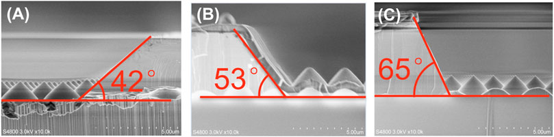
FIGURE 2. (color online) The SEM of tapered sidewalls after etching by ICP with an inclination of 42° (A), 53° (B), and 65° (C) to the horizontal.
Figure 3 shows the transmittance of the ITO thin films prepared by epitaxial and the reflectivity of the reflective mirror composed of epitaxial ITO/Al, respectively. The epitaxial ITO thin film exhibits 93.6% high optical transmittance at 365 nm. This phenomenon can be partially attributed to the better quality and unique structural property of the epitaxial ITO thin film grown by MOCVD. Z. Chen et al. also gave a detailed theoretical explanation on why the epitaxial ITO material has high transmittance in our previous published paper (Zhang et al., 2018). It is necessary to propose that the ITO material required for the flip-chip LED needs to have an excellent surface smoothness to obtain a high reflectance. The surface morphology of ITO can be changed by optimizing the MOCVD growth conditions. The inserted image in Figure 3 was the surface morphology SEM of epitaxial ITO grown on an LED epitaxial wafer, taken with Hitachi S-4800 SEM, which shown a moderate flat surface suitable for metal mirror deposition to get high reflectivity. The resistivity and mobility of epitaxial ITO film was
Where n is the ideality factor, k the Boltzmann constant, T the absolute temperature and e the elementary charge. The Rs is obtained from the linear area of the I-V curve. The lower series resistance of flip-chip UV-LED proved that the contact between ITO and p-AlGaN shows good ohmic characteristics. The structure of flip-chip UV-LED has better current spreading. The inserted image in Figure 5 (labeled as “Sample 1”) is the photograph of the bare LED chip driven by 20 mA current.
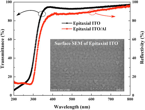
FIGURE 3. (color online) The transmittance of the epitaxial ITO film and reflectivity of the epitaxial ITO/Al layers and the inserted image was the surface morphology SEM of epitaxial ITO grown on the LED epitaxial wafer.
For comparison, we design and fabricate four types of HV-LEDs consist of 1 × 2 A1, A2, B1, B2 micro-cells shown in Figure 4, respectively. Meanwhile, to avoid the influence of the process on device test results, the HV-LEDs are fabricated on the same wafer, and the number of chips in each HV-LEDs category was not less than 25. Also, the HV-LEDs was fabricated in the first deposited SiO2 with a thickness of 700 and 1,000 nm, respectively. Figure 4 illustrated the backside of the luminous photograph, and the double test probe was applied to p- and n-electrodes of LED with a 50 mA currents input. Table 1 lists the typical electrical parameters of HV-LED. Under injection currents of 350mA, the forward voltages (Vf) of 1 × 2 A1, 1 × 2 A2, 1 × 2 B1, and 1 × 2 B2 HV-LEDs with a SiO2 thickness of 700 nm was measured to be 9.79, 9.60, 9.48, and 9.02 V, respectively. When the thickness of SiO2 increases from 700 to 1,000 nm, the forward voltages (Vf) of HV-LEDs decreases by 0.53–0.78 V, and the corresponding Vf was 9.25, 9.07, 8.70, and 8.35 V, respectively. Also, we measured the reverse leakage current (IR) of all HV-LED samples in each HV-LEDs category and calculated the yield of reverse leakage current (yield %), which is defined as the reverse leakage current less than 2 μA under the reverse voltage −5 V. The corresponding yield of IR data is shown in Table 1. The IR yield of HV-LEDs with 1,000 nm thickness of SiO2 is generally over 90%, and this value is 1–17 percentage points higher than that of LED with 700 nm thickness of SiO2. Thus, it can be seen that the I-V and reverse leakage current characteristics of HV-LED are influenced by the thickness of first deposited SiO2 passivation layer. This is because, with the increase of SiO2 thickness, the leakage channels between metal electrodes and AlGaN are reduced. On the other hand, it also provides a flat interface for metal evaporation and reduces the resistance of interconnected electrodes. Meanwhile, among the four groups of HV-LEDs, 1 × 2 B2 HV-LEDs with 1,000 nm thickness of SiO2 has the lowest working voltage of 8.35 V and the highest IR yield of 96%. This indicates that the electrode structure composed of n-finger mesa and interdigitated p-finger provides the better current spreading ability and smaller series resistance (Rs) of 3.52 Ω shown in Figure 5 (labeled as “Sample 2”). Therefore, B2 micro-cells was used in the design of 2 × 2 HV-LED chip, and the inset image (labeled as “Sample 3”) in the Figure 5 demonstrated the HV-LED device structure, and the double test probe was applied to a symmetrical electrode of HV-LED with a 50 mA currents input.
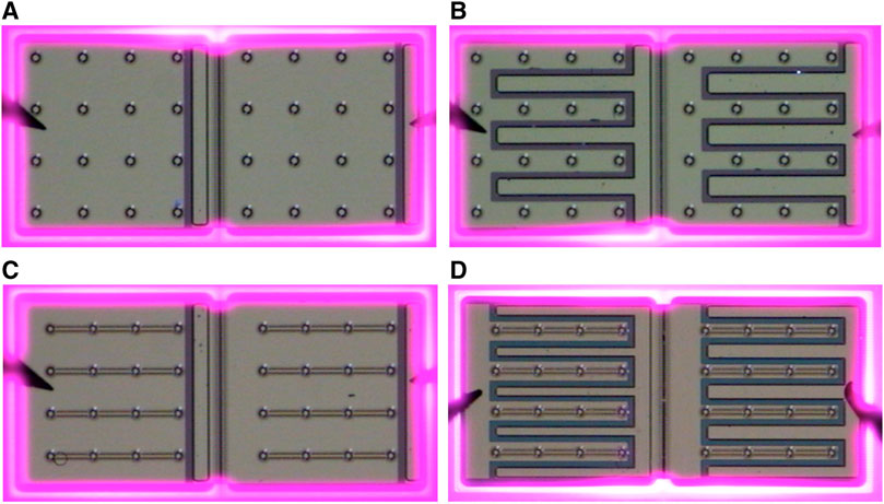
FIGURE 4. (color online) Images were taken by optical microscopy of 1 × 2 micro-cells for HV-LED driven by 50 mA forward currents: (A) (1 × 2 A1), (B) (1 × 2 A2), (C) (1 × 2 B1), (D) (1 × 2 B2).
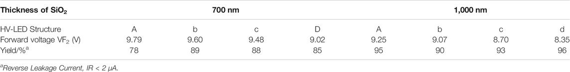
TABLE 1. Measured electrical parameters of HV-LED with different SiO2 thickness driven at 350 mA. A (1 × 2 A1), B (1 × 2 A2), C (1 × 2 B1), D (1 × 2 B2).
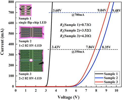
FIGURE 5. (color online) I-V characteristic for single micro-cells (Sample 1), 1 × 2 B2 micro-cells (Sample 2) and 2 × 2 B2 micro-cells (Sample 3). The inserted map is the LED image driven at current (symmetrical electrode side up).
In order to further investigate the electrical characteristics of HV-LEDs with different number of micro-cells, we compare the I-V characteristics for the fabricated single micro-cells (labeled as “Sample 1”), 1 × 2 B2 micro-cells (labeled as “Sample 2”) and 2 × 2 B2 micro-cells (labeled as “Sample 3”) with the current increases from 0 to 800 mA, as shown in Figure 5. Under injection currents of 350 and 700 mA, the forward voltages (Vf) of Sample 1, Sample 2, and Sample 3 was measured to be 3.43 and 3.60 V, 8.35 and 9.48 V, 7.86 and 9.04 V, respectively. The corresponding series resistance (Rs) of the HV-LEDs was 0.73, 3.52, and 4.20 Ω, respectively. High voltage LED can be seen as a circuit with a series-parallel connection by a micro-cell LED. For instance, Sample 2 can be regarded as a series connection of two sample 1 using the equivalent circuit Diagram. Theoretically, the series resistance (Rs) of Sample 2 should be about twice that of Sample 1. The excess series resistance (2.06 Ω) comes from the additional resistance generated by the interconnected electrodes, and it can be reduced or eliminated by thickening interconnected electrodes and optimizing the length of interconnected electrodes.
4 Conclusion
In summary, we have developed and shown high-performance and high-power near-ultraviolet (UV) flip-chip high-voltage light-emitting diodes (LEDs) based on AlGaN operating at 368 nm using an epitaxial indium tin oxide (ITO)/aluminum reflecting mirror and symmetry electrode configuration. ITO thin films grown through MOCVD displayed a transmittance of up to 93.6% at 365 nm and a reflectance of 81.2% in epitaxial ITO/Al. Meanwhile, we designed and characterised a series of high-voltage LED microcells with changeable n-type mesa structures and p-type connecting electrodes. The enhanced high-voltage LED features a lower forward voltage, which makes it suitable for high-power applications.
Data Availability Statement
The original contributions presented in the study are included in the article/supplementary material, further inquiries can be directed to the corresponding authors.
Author Contributions
CM: Experiment, Data curation, Discussion, Writing. XW: Experiment, Data curation. YL: Experiment. JY: Data curation. GC: Discussion. GW: Conceptualization, Discussion. BF: Conceptualization, Discussion, Writing.
Funding
The authors gratefully acknowledge the support of Fund of Research Fund of Guangdong-Hong Kong-Macao Joint Laboratory for Intelligent Micro-Nano Optoelectronic Technology under Grant 2020B1212030010, Key laboratory of semiconductor micro display of Guangdong province under Grant 2020B121202003, Guangdong Province Science and Technology Department Project under Grant 2019TQ05Z829, Educational Commission of Guangdong Province under Grant 2020ZDZX2043, and Grant 2020KZDZX1207.
Conflict of Interest
The authors declare that the research was conducted in the absence of any commercial or financial relationships that could be construed as a potential conflict of interest.
Publisher’s Note
All claims expressed in this article are solely those of the authors and do not necessarily represent those of their affiliated organizations, or those of the publisher, the editors and the reviewers. Any product that may be evaluated in this article, or claim that may be made by its manufacturer, is not guaranteed or endorsed by the publisher.
References
Chen, Z., Zhuo, Y., Tu, W., Ma, X., Pei, Y., Wang, C., et al. (2017). Highly Ultraviolet Transparent Textured Indium Tin Oxide Thin Films and the Application in Light Emitting Diodes. Appl. Phys. Lett. 110, 1600320–1601570. doi:10.1063/1.4986452
Choi, C.-H., Han, J., Park, J.-S., and Seong, T.-Y. (2013). Near Ultraviolet InGaN/AlGaN-Based Light-Emitting Diodes with Highly Reflective Tin-Doped Indium oxide/Al-Based Reflectors. Opt. Express 21 (22), 26774–26779. doi:10.1364/oe.21.026774
Chong, W. C., and Lau, K. M. (2014). Performance Enhancements of Flip-Chip Light-Emitting Diodes with High-Density N-type point-contacts. IEEE Electron. Device Lett. 35 (10), 1049–1051. doi:10.1109/led.2014.2349956
Khan, A., Balakrishnan, K., and Katona, T. (2008). Ultraviolet Light-Emitting Diodes Based on Group Three Nitrides. Nat. Photon 2, 77–84. doi:10.1038/nphoton.2007.293
Kim, D.-H., Han, J., and Seong, T.-Y. (2014). Use of Graphene for Forming Al-Based P-type Reflectors for Near Ultraviolet InGaN/AlGaN-Based Light-Emitting Diode. Curr. Appl. Phys. 14, 1176–1180. doi:10.1016/j.cap.2014.06.012
Kneissl, M., Kolbe, T., Chua, C., Kueller, V., Lobo, N., Stellmach, J., et al. (2011). Advances in Group III-Nitride-Based Deep UV Light-Emitting Diode Technology. Semicond. Sci. Technol. 26, 014036(2)–014036(5). doi:10.1088/0268-1242/26/1/014036
Kuo, S., Hong, K., and Lu, T. (2015). Enhanced Light Output of UVA GaN Vertical LEDs with Novel DBR Mirrors. IEEE J. Quan. Electron 51 (12), 3300805. doi:10.1109/jqe.2015.2502901
Lin, Y. H., Liu, Y. S., and Liu, C. Y. (2010). Light Output Enhancement of Near UV-LED by Using Ti-Doped ITO Transparent Conducting Layer. IEEE Photon. Technol. Lett. 22 (19), 1443–1445. doi:10.1109/lpt.2010.2056363
Lin, W.-Y., Wang, T.-Y., Ou, S.-L., Liang, J.-H., and Wuu, D.-S. (2014). Improved Performance of 365-nm LEDs by Inserting an Un-doped Electron-Blocking Layer. IEEE Electron. Device Lett. 35 (4), 467–469. doi:10.1109/led.2014.2306711
Liu, C.-Y., Huang, C.-Y., Wu, P.-Y., Huang, J.-K., Kao, T. S., Zhou, A.-J., et al. (2016). High-Performance Ultraviolet 385-nm GaN-Based LEDs with Embedded Nanoscale Air Voids Produced through Atomic Layer Deposition and Al2O3Passivation. IEEE Electron. Device Lett. 37 (4), 452–455. doi:10.1109/led.2016.2532352
Lobo, N., Rodriguez, H., Knauer, A., Hoppe, M., Einfeldt, S., Vogt, P., et al. (2010). Enhancement of Light Extraction in Ultraviolet Light-Emitting Diodes Using Nanopixel Contact Design with Al Reflectorflector. Appl. Phys. Lett. 96, 081109. doi:10.1063/1.3334721
Mukai, T., and Nakamura, S. (1999). Ultraviolet InGaN and GaN Single-Quantum-Well-Structure Light-Emitting Diodes Grown on Epitaxially Lat-Erally Overgrown GaN Substrates. Jpn. J. Appl. Phys. 38 (10), 5735–5739. doi:10.1143/jjap.38.5735
Muramoto, Y., Kimura, M., and Nouda, S. (2014). Development and Future of Ultraviolet Light-Emitting Diodes: UV-LED Will Replace the UV Lamp. Semicond. Sci. Technol. 29, 084004. doi:10.1088/0268-1242/29/8/084004
Nakashima, T., Takeda, K., Shinzato, H., Iwaya, M., Kamiyama, S., Takeuchi, T., et al. (2013). Combination of Indium-Tin Oxide and SiO2/AlN Dielectric Multilayer Reflective Electrodes for Ultraviolet-Light-Emitting Diodes. Jpn. J. Appl. Phys. 52, 08JG07 1–08JG07 3. doi:10.7567/jjap.52.08jg07
Shatalov, M., Sun, W., Lunev, A., Hu, X., Dobrinsky, A., Bilenko, Y., et al. (2012). AlGaN Deep-Ultraviolet Light-Emitting Diodes with External Quantum Efficiency above 10%. Appl. Phys. Exp. 5 (8), 082101. doi:10.1143/apex.5.082101
Svensk, O., Törmä, P. T., Suihkonen, S., Ali, M., Lipsanen, H., Sopanen, M., et al. (2008). Enhanced Electroluminescence in 405nm InGaN/GaN LEDs by Optimized Electron Blocking Layer. J. Cryst. Growth 310 (23), 5154–5157. doi:10.1016/j.jcrysgro.2008.07.025
Takehara, K., Takeda, K., Ito, S., Aoshima, H., Iwaya, M., Takeuchi, T., et al. (2012). Indium-Tin oxide/Al Reflective Electrodes for Ultraviolet Light-Emitting Diodes. Jpn. J. Appl. Phys. 51, 042101 1–042101 4. doi:10.1143/jjap.51.042101
Tien, C.-H., Kuo, C.-H., Wuu, D.-S., and Horng, R.-H. (2017). Improved Optoelectronic Performance of High-Voltage Ultraviolet Light-Emitting Diodes through Electrode Designs. IEEE Trans. Electron. Devices 64 (11), 4526–4531. doi:10.1109/ted.2017.2750704
Wang, C. H., Lin, D. W., Lee, C. Y., Tsai, M. A., Chen, G. L., Kuo, H. T., et al. (2011). Efficiency and Droop Improvement in GaN-based High-Voltage Light-Emitting Diodes. IEEE Electron. Device Lett. 32 (8), 1098–1100. doi:10.1109/led.2011.2153176
Wu, P.-C., Ou, S.-L., Horng, R.-H., and Wuu, D.-S. (2017). Improved Performance and Heat Dissipation of Flip-Chip white High-Voltage Light Emitting Diodes. IEEE Trans. Device Mater. Relib. 17 (1), 197–203. doi:10.1109/tdmr.2016.2646362
Wu, P.-C., Ou, S.-L., Horng, R.-H., and Wuu, D.-S. (2017). Improved Performance of High-Voltage Vertical GaN LEDs via Modification of Micro-cell Geometry. Appl. Sci. 7 (6), 506. doi:10.3390/app7060506
Zhang, Y., Ding, M., Zhao, D., Huang, H., Huang, L., Lin, Y., et al. (2018). Analysis and Modeling of thermal-electric Coupling Effect of High-Power Monolithically Integrated Light-Emitting Diode. IEEE Trans. Electron. Devices 65 (2), 564–571. doi:10.1109/ted.2017.2783622
Keywords: ultraviolet light-emitting diode (LEDs), flip-chip, AlGaN, indium tin oxide (ITO)/Al reflective mirror, 365-nm, high-voltage
Citation: Ma C, Wang X, Lao Y, Yang J, Chen G, Wang G and Fan B (2022) Design and Performance of Ultraviolet 368-nm AlGaN-Based Flip-Chip High-Voltage LEDs with Epitaxial Indium Tin Oxide/Al Reflective Mirror and Symmetry Electrode Arrangement. Front. Mater. 9:836714. doi: 10.3389/fmats.2022.836714
Received: 15 December 2021; Accepted: 11 February 2022;
Published: 28 February 2022.
Edited by:
Longxing Su, ShanghaiTech University, ChinaReviewed by:
Yu Zhao, Guangdong University of Technology, ChinaHock Jin Quah, University of Science Malaysia, Malaysia
Copyright © 2022 Ma, Wang, Lao, Yang, Chen, Wang and Fan. This is an open-access article distributed under the terms of the Creative Commons Attribution License (CC BY). The use, distribution or reproduction in other forums is permitted, provided the original author(s) and the copyright owner(s) are credited and that the original publication in this journal is cited, in accordance with accepted academic practice. No use, distribution or reproduction is permitted which does not comply with these terms.
*Correspondence: Gang Wang, c3Rzd2FuZ2dAbWFpbC5zeXN1LmVkdS5jbg==; Bingfeng Fan, ZmFuYmluZ2ZAZm9zdS5lZHUuY24=