 L. Zhao
 W. H. Ng
 A. P. Knights
 D. V. Stevanovic2
 D. J. Mannion
 A. Mehonic
 A. J. Kenyon
- 1Department of Electronic and Electrical Engineering, University College London, London, United Kingdom
- 2Department of Engineering Physics, McMaster University, Hamilton, ON, Canada
We report that implanting argon ions into a film of uniform atomic layer deposition (ALD)-grown SiOx enables electroforming and switching within films that previously failed to electroform at voltages <15 V. We note an implantation dose dependence of electroforming success rate: electroforming can be eliminated when the dosage is high enough. Our devices are capable of multi-level switching during both set and reset operations, and multiple resistance states can be retained for more than 30,000 s under ambient conditions. High endurance of more than 7 million (7.9 × 10⁶) cycles is achieved alongside low switching voltages (±1 V). Comparing SiOx fabricated by this approach with sputtered SiOx we find similar conduction mechanisms between the two materials. Our results show that intrinsic SiOx switching can be achieved with defects created solely by argon bombardment; in contrast to defects generated during deposition, implantation generated defects are potentially more controllable. In the future, noble ion implantation into silicon oxide may allow optimization of already excellent resistance switching devices.
Introduction
Redox-based random access memory (ReRAM) has for some time been considered as a potential replacement for flash memory, attracting significant research effort since the beginning of the century (Lee et al., 2015). More recently, ReRAM has also been intensely studied as an elementary component for novel computing architectures (Ielmini and Wong 2018; Zarudnyi et al., 2018; Marzec et al., 2019; Mehonic et al., 2020). ReRAM excels in properties such as endurance, power consumption, and read/write speed (Lee et al., 2011; Feng et al., 2016; Böttger et al., 2020). Most ReRAM devices are of simple two-terminal metal-insulator-metal (MIM) structure. Such structural simplicity and ease of fabrication allow ReRAM to stand out from competing memory technologies.
The insulating layer in ReRAM devices is key to device performance. The most common switching materials are transitional metal oxides such as TaOx, HfOx and TiOx (Lee et al., 2011; Feng et al., 2016; Trapatseli et al., 2016). ReRAM devices based on silicon oxide (SiOx) has attracted attention in recent years. In some aspects, SiOx has its own material advantages over the transitional metal oxides. For example, the growth of SiOx thin film are simpler and easier to control compare to most transitional metal oxides since there is less variety of silicon oxide stoichiometry. SiOx based ReRAM devices typically have better performance stability at elevated temperatures, and larger LRS and HRS contrast. This is due to SiOx having a higher bandgap compared to TaOx and HfOx (Mehonic et al., 2018).
Importantly, silicon oxide offers superior compatibility with existing complementary metal–oxide–semiconductor (CMOS) technology. In the early 2010’s, Yao et al., Mehonic et al., and Wang et al. reported ReRAM devices based on silicon oxide material. Yao et al. and Wang et al. reported their devices were operating under vacuum conditions (Yao et al., 2010; Wang et al., 2012). By contrast, Mehonic et al. reported their devices were operating under ambient conditions (Mehonic et al., 2012). This was mainly due to the fact that the conductive filament formed within the silicon oxide layer rather than on the outer surface. Previously, we have demonstrated high performance SiOx based ReRAM devices (Mehonic et al., 2017). Detailed performance comparison between SiOx and other transitional oxide based ReRAM can be found in our review article (Mehonic et al., 2018). Note that these devices are of intrinsic and filamentary nature: that is, conduction is modulated by the reversible formation of conductive oxygen vacancy filaments under the application of an external field (Mehonic and Kenyon 2015).
Our previous SiOx ReRAM devices were grown by reactive sputtering, which induces oxide microstructure critical for efficient resistance switching (Munde et al., 2017). Layers grown by sputtering tend to have columnar microstructure thanks to shadowing effects during deposition (Thornton 1986; McCann et al., 2011). Internal column boundaries structures are defect rich sites, which serve as nucleation points for the growth of oxygen vacancy filaments under electrical bias (Jin and Chang 2001; Mehonic et al., 2016). However, control of these columnar structures relies on a combination of sputtering parameters and roughness of the bottom electrode, and hence is stochastic in nature. Here we demonstrate that implanting noble gas ions into electrically inert SiOx enables reliable control of defect generation, and hence switching performance.
Ion implantation has been employed previously to improve ReRAM performance. The common effects of ion implantation in ReRAM are reduced variability in switching parameters and reduced electroforming voltages. Depending on the species of implanted ions, these improvements can be attributed to doping effects or impact-induced structural change (Liu et al., 2009; Zhang et al., 2011; Mikhaylov et al., 2019). If the implanted ions are reactive, the ions can assist formation of conductive filaments by reacting with the host material (Liu et al., 2009; Zhang et al., 2011). Alternatively, implantation of noble ions will only change the structure of the host material (Ku et al., 2019; Mikhaylov et al., 2019).
We chose Ar ions for implantation to limit the effect of implantation to structural change. One key difference of our work report here from previous literature is that our SiOx layer is electrical inert and cannot electroform even when swept to high voltage (−15 V), whereas most reported work starts from a switchable material. For example, Mikhaylov et al. implanted Xe+ ions into switchable sputtered silicon oxide to form preferential pathways for filament formation (Mikhaylov et al., 2019). By confining the location of conductive filament, they reported reduced variation in electroforming voltage. However, there is no detailed description of the switching performance, and the switching voltages are relatively high (∼3 V). Another key difference is that switching in our devices depends largely on implantation created defects, so we allow ions to penetrate throughout the switching layer, whereas Mikhaylov et al. implanted Xe+ ions to a maximum depth of 9 nm in a 40 nm thick SiOx layer.
Materials and Methods
All devices used in this work have simple MIM structure, each with an identical electrode configuration. The top electrode is 100 nm of gold on a 5 nm titanium wetting layer, deposited by electron beam evaporation. The bottom electrode is 100 nm of molybdenum, deposited by magnetron sputtering (300 W, 5 m Torr Capman pressure). For ion implanted devices, top electrodes were deposited after the oxide switching layers were implanted with argon.
All SiOx ReRAM devices mentioned in this work were grown on silicon substrates with 1 μm of thermal oxide on top. The SiOx switching layer were grown by ALD or magnetron sputtering. For ALD-grown SiOx, the precursers used were tris(dimethylamino)silicon and ozone. The deposition temperature was 200°C. For sputtered SiOx, it was grown by magnetron sputtering with RF power of 110W, 3mTorr of Capman pressure and a Ar:O2 ratio of 1:1.
We investigated three types of switching layer, all with nominally identical thicknesses of 30 nm: 1) ALD-grown SiOx; 2) ALD-grown SiOx implanted with Ar ions; 3) Sputtered SiOx. Specific implantation fluences are given in Table 1, while the sputtered samples act as controls to allow comparison with our previously reported devices.

TABLE 1. Nominal implantation fluence for different samples.
The implanted samples were irradiated at room temperature in a vacuum of approximately 10−6 Torr. The ion beam was scanned over an area of 5 cm2. The beam current on the sample was between 1 and 2 uA during implantation. The non-uniformity of implantation dose across the sample is <5%.
Electrical characterization was performed with a Keithley 4200 Semiconductor Characterization System. Endurance testing used a pulse measuring unit (PMU), while all other electrical tests used a source measuring unit (SMU). During setting and electroforming with SMU, a TP2104 N3 enhancement mode PFET was connected in series to limit the maximum current through the device under test. All electrical tests conducted in ambient conditions unless otherwise specified. All devices tested in this work had 400 × 400 µm top contacts.
While the types of defects induced by implantation can be complex, we simulated a representation of atomic damage profile generated by 17 keV argon bombardment of 30 nm of silicon dioxide. SRIM simulation shows that most of defects generated are within the silicon dioxide layer (Figure 1).
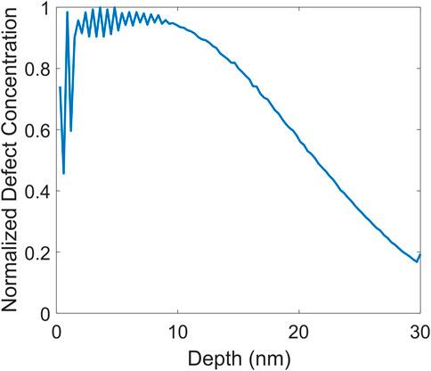
FIGURE 1. SRIM simulated atomic damage profile in 30 nm of SiO2 after implantation with Ar at an energy of 17 keV.
To achieve electroforming, all devices were swept from 0 to −15V, with the maximum current through the circuit limited to 1 mA by a transistor connected in series.
Results and Discussion
ALD-grown SiOx is more resistive than sputtered SiOx. Figure 2 shows the I-V sweep of a pristine ALD-grown SiOx device and the I-V sweep of a pristine sputtered SiOx device. Such high resistance indicates lower concentration of defects in ALD-grown SiOx, which can be explained by the absence of columnar microstructure in ALD-grown SiOx device. In space-charge-limited conduction (SCLC), current is proportional to the square of applied voltage (Chiu 2014). According to inset of Figure 2, space-charge-limited conduction (SCLC) is the dominating conduction mechanism before negative differential resistance was observed, hence, the negative differential resistance observed in sputtered SiOx from −4 to −10 V could be a result of charge trapping.
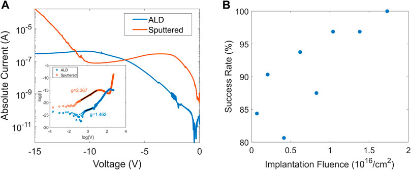
FIGURE 2. (A) Electrical sweep of a pristine ALD-grown SiOx device and a pristine sputtered SiOx device. ALD-grown SiOx is less resistive due to lower concentration of defects. Charge trapping or polarization could be the cause of negative differential resistance observed in sputtered SiOx. Inset shows SCLC fitting of the two types of SiOx pristine states. In sputtered SiOx, SCLC is the dominating conduction mechanism before the negative differential resistance appears, supporting the hypothesis that negative differential resistance is caused by charge trapping. (B) Correlation between implantation fluence and electroforming success rate when Ar+-implanted devices were swept to −15 V, each data point includes 31 or 32 devices. As implantation fluence increases, the electroforming success rate increases accordingly.
Before ion implantation, electroforming is hardly possible in ALD-grown SiOx. Among 32 devices, only 1 electroformed to a low resistance state (LRS), which is lower than 10 kΩ. By contrast, the average electroforming success rate in implanted SiOx increases as implantation fluence increases; Figure 2B shows the correlation between electroforming success rate and implantation fluence. For the 32 devices in sample H with maximum implantation fluence of 1.73 × 10¹⁶ ions/cm2, 13 devices were effectively forming free in which they were already in the LRS when first measured. In any case, sweeping the applied voltage to −15 V caused all remaining devices to electroform.
A lower electroforming voltage also means smaller fluctuations. The electroforming voltage standard deviation for sample H (the highest fluence: 1.73 × 10¹⁶ ions/cm2) is 0.55 V. In comparison, the sputtered sample has average electroforming voltage of −9.89 V with a standard deviation of 4.19 V.
Excellent switching can be achieved in implanted samples; Figure 3A shows 10 switching cycles of a device from sample G (fluence: 1.38 × 10¹⁶ions/cm2). Devices from samples with higher fluences has similar switching voltages. Figure 3B shows the cumulative switching voltages of an implanted device from sample H (fluence: 1.73 × 10¹⁶ ions/cm2). The device sets between −0.8 V and −1.2 V and resets around +1 V. These values are similar to those previously reported for sputtered SiOx devices (Mehonic et al., 2017). Our observation shows a strong correlation between low cycle-to-cycle variability and endurance; the highly uniform switching in Figure 3A allows the same device to achieve high endurance in Figure 3C,E.
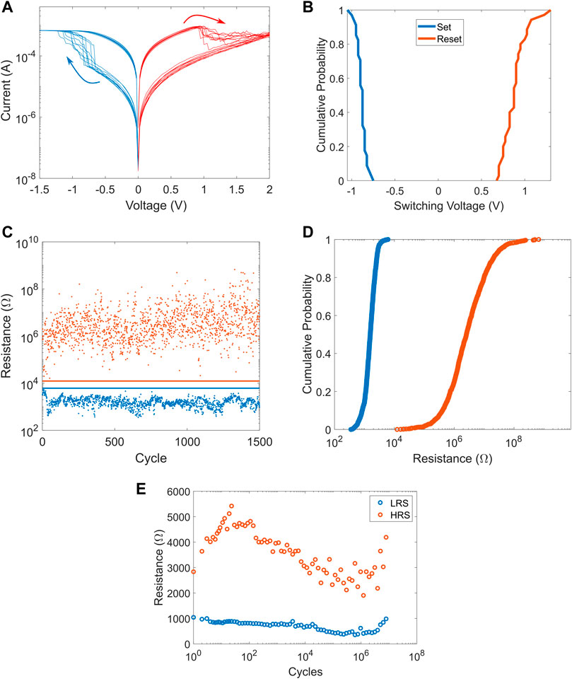
FIGURE 3. (A) I-V switching curves of an implanted ALD-grown SiOx device. (B) Cumulative probability of switching voltages of an implanted ALD-grown SiOx device. (C) Cycling of the same device from Figure 3a with SMU. The blue line indicates the upper limit of the LRS; the red line is the lower limit of the HRS, there are no data points between the two lines, indicating 100% success rate across 1500 switching cycles. (D) Cumulative probability of the two resistance states. (E) Switching of the same device from Figure 3a using a PMU. Blue dots represent LRS and orange dots represent HRS.
Figure 3C shows 1500 switching cycles of a device from sample G. Switching is achieved with a SMU. Applied set and reset voltages were −3 and 2.5 V, respectively. These switching voltages are higher than sweep-triggered switching voltages in Figure 3A, and these high switching voltages were used to ensure 100% success rate; this is possible because current overshoot is effectively suppressed by the transistor in series.
High switching voltages bring the benefit of high on/off resistance ratio. On average, there is more than 4 orders of magnitude contrast between the LRS and the high resistance state (HRS), this is shown in Figure 3D. We further analyzed the uniformity of resistance states; the relative standard deviation for LRS is 0.431 and HRS is 3.58; the LRS is more uniform than previously reported sputtered SiOx (Mehonic et al., 2017), but the HRS shows high variability due to high reset voltages.
For cycling endurance testing, resistances were recorded with logarithmic time spacing to avoid data overload. Fast pulses were used to minimize measurement duration. Figure 3E shows the same device from Figure 3C cycling for over 7 million cycles. Note that the device still switches at the end of the test, implying more cycles are possible. The pulses used were: −2.2V, 300 ns for set, 2.4 V, 50 µs for reset. Switching with pulses produces a smaller resistance window than switching with SMU. This is because the transistor used cannot respond rapidly to fast pulses, and hence less energy is now supplied to avoid current overshoot.
As applications for ReRAM shift towards novel computing architectures such as those of interest to neuromorphic computing (Joksas et al., 2020), the importance of multilevel switching grows. We demonstrated multilevel switching in our implanted SiOx devices using two methods: changing the reset stop voltage and changing the voltage applied to the serial transistor gate.
Figure 4A shows two more intermediate resistance states besides the LRS and HRS; by varying the reset stop voltage from 1.2 to 2 V, the device resistance changes from 5.7 to 69 kΩ. As reset stop voltage increases, we hypothesise that the higher energy input results in more filament dissolution, and different resistance levels correspond to different filament thicknesses.
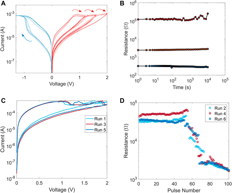
FIGURE 4. (A) Multiple resistance states achieved in an implanted SiOx device by changing the stop voltages in the reset sweep. (B) Multiple resistance states in an implanted SiOx device lasting more than 30,000 s (C) and (D) shows gradual resistance programming of an implanted SiOx device. Devices are reset by voltage sweeps (C) and set by voltage pulses (D). Data are shown for three consecutive set and reset cycles. The device is set to LRS by applying voltage pulses to the gate of serial transistor; the magnitude of the voltage pulse increases linearly as pulse number increases during set.
We further confirmed the stability of multiple resistance states. Figure 4B shows the retention data for three resistance levels. Resistance is always measured at 0.3 V and the time intervals between reads are spaced logarithmically, this is done to avoid data overload and possible resistance state disturbance by constant voltage application. All three states were stable for more than 3 × 10⁴ s.
We achieved repeatable multiple resistance states for implanted SiOx devices by varying the voltage applied to the serial transistor gate, similar to a method reported by Hu et al (Hu et al., 2018). Because the gate voltage regulates the maximum current through the device, by increasing gate voltage we increase the thickness of the conductive filament.
Figure 4D shows three consecutive cycles of resistance programming under identical programming conditions. Before each cycle, the device is reset to its HRS by sweeping from 0 to 2 V (Figure 4C). During set programming (Figure 4D), −3 V is applied to the top electrode and the bottom electrode is grounded. Pulse magnitude applied to the gate increases linearly from −1.2 to −1.5 V as pulse number increases, and the duration of every pulse is 2 µs long. To read resistance states, the transistor voltage is kept at −1.5 V, and 0.3 V is applied to device top electrode.
Multi-level switching achieved by varying gate voltage is not only consistent from cycle-to-cycle, but also there is good linearity from pulse 55 to pulse 100, which can be very useful in implementing ReRAM based neural networks (Mehonic et al., 2019). There is little change of device resistance from the first pulse to pulse 55, similar behavior was reported before (Hu et al., 2018). Additionally, we used a moderate transistor gate voltage to avoid hard breakdown; by exploring higher voltage ranges and decrease voltage step sizes, even more resistance states could be realized.
We examined conduction mechanisms in the different resistance states of implanted SiOx devices, comparing them to those exhibited by the sputtered SiOx sample. We find that, despite differences in resistance values, Ohmic conduction appears to dominate the LRS in both types of silicon oxide. The current and voltage are linearly correlated, and linear correlation is observed in a log-log plot with slopes close to unity (Figure 5A).
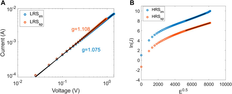
FIGURE 5. (A) Fitting of LRS I-V curves in a log-log plot, LRSsp is the LRS from sputtered SiOx and LRSim is the LRS from implanted ALD-grown SiOx. (B) Thermionic emission fitting of HRS I-V curves.
In the HRS, conduction is achieved via thermionic emission (Figure 5B). We fitted the HRS I-V curves to thermionic emission, the standard fitting expression can be found in literature (Lim and Ismail 2015), and the extracted dielectric constants of 5.39 and 7.69 are consistent with silicon suboxide.
These results are different from previously reported intrinsic bipolar SiOx ReRAM devices. Ng et al. (2018) and Mehonic et al. (2012) report trap-assisted tunnelling (TAT) to be the dominant conduction mechanism, but TAT may be less important in our devices because of lower applied field or differences in microstructure and the distribution of defects within the oxide.
Based on these results, we propose that conduction in both types of SiOx devices is achieved by continuous oxygen vacancy filament in the LRS. During reset, the filament near the electrode/filament interface is oxidized, and conduction is limited by thermionic emission in the HRS.
Conclusion
In conclusion, we have demonstrated that implanting uniform SiOx with noble gas ions can enable electroforming and result in devices that exhibit high performance resistance switching. This includes low switching voltages, high cycling endurance and long state retention times. Importantly, we demonstrate that Ar+-implanted intrinsic SiOx ReRAM devices can reliably achieve and retain multiple resistance levels, showing the potential of intrinsic SiOx ReRAM devices as basic element for artificial neural networks and multilevel memories. We have also demonstrated that the electroforming process is strongly related to implantation fluence, and our intrinsic SiOx ReRAM devices already show comparable performance to more optimised sputtered SiOx ReRAM devices. We show that this fabrication method has the potential to produce more uniform and controllable ReRAM devices.
Data Availability Statement
The raw data supporting the conclusions of this article will be made available by the authors, without undue reservation.
Author Contributions
AJK, LZ, and WHN conceived the idea and designed the study. WHN and LZ were responsible for sample fabrication. LZ and DJM performed experimental measurements and the SRIM simulation. APK and DVS performed the ion implantation. AM contributed to the understanding of the electrical behaviour of the memristor devices. LZ and WHN co-wrote the initial draft of the manuscript with contribution from all the co-authors. All authors contributed to the discussion and improvement of the manuscript. AJK and WHN oversaw the project.
Funding
AM acknowledges funding from the Royal Academy of Engineering under the Research Fellowship Scheme. AJK gratefully acknowledges funding from the Engineering and Physical Sciences Research Council (EP/P013503/1 and EP/K01739X/1) and the Leverhulme Trust (RPG-2016–135).
Conflict of Interest
AJK and AM are founders and directors of Intrinsic Semiconductor Technologies Ltd., a spin-out company commercialising silicon oxide ReRam. WHN is a consultant to, and shareholder in, Intrinsic.
The remaining authors declare that the research was conducted in the absence of any commercial or financial relationships that could be construed as a potential conflict of interest.
Publisher’s Note
All claims expressed in this article are solely those of the authors and do not necessarily represent those of their affiliated organizations, or those of the publisher, the editors, and the reviewers. Any product that may be evaluated in this article, or claim that may be made by its manufacturer, is not guaranteed or endorsed by the publisher.
References
Böttger, U., von Witzleben, M., Havel, V., Fleck, K., Rana, V., Waser, R., et al. (2020). Picosecond Multilevel Resistive Switching in Tantalum Oxide Thin Films. Sci. Rep. 10, 16391. doi:10.1038/s41598-020-73254-2
Chiu, F.-C. (2014). A Review on Conduction Mechanisms in Dielectric Films. Adv. Mater. Sci. Eng. 2014, 1–18. doi:10.1155/2014/578168
Feng, W., Shima, H., Ohmori, K., and Akinaga, H. (2016). Investigation of Switching Mechanism in HfOx-ReRAM Under Low Power and Conventional Operation Modes. Sci. Rep. 6, 1–8. doi:10.1038/srep39510
Hu, M., Graves, C. E., Li, C., Li, Y., Ge, N., Montgomery, E., et al. (2018). Memristor‐Based Analog Computation and Neural Network Classification with a Dot Product Engine. Adv. Mat. 30, 1705914. doi:10.1002/adma.201705914
Ielmini, D., and Wong, H.-S. P. (2018). In-Memory Computing with Resistive Switching Devices. Nat. Electron. 1, 333–343. doi:10.1038/s41928-018-0092-2
Jin, Y.-G., and Chang, K. J. (2001). Mechanism for the Enhanced Diffusion of Charged Oxygen Ions in SiO2. Phys. Rev. Lett. 86, 1793–1796. doi:10.1103/PhysRevLett.86.1793
Joksas, D., Freitas, P., Chai, Z., Ng, W. H., Buckwell, M., Li, C., et al. (2020). Committee Machines-A Universal Method to Deal with Non-Idealities in Memristor-Based Neural Networks. Nat. Commun. 11, 1–10. doi:10.1038/s41467-020-18098-0
Ku, B., Abbas, Y., Kim, S., Sokolov, A. S., Jeon, Y.-R., and Choi, C. (2019). Improved Resistive Switching and Synaptic Characteristics Using Ar Plasma Irradiation on the Ti/HfO2 Interface. J. Alloys Compd. 797, 277–283. doi:10.1016/j.jallcom.2019.05.114
Lee, J. S., Lee, S., and Noh, T. W. (2015). Resistive Switching Phenomena: A Review of Statistical Physics Approaches. Appl. Phys. Rev. 2, 031303. doi:10.1063/1.4929512
Lee, M.-J., Lee, C. B., Lee, D., Lee, S. R., Chang, M., Hur, J. H., et al. (2011). A Fast, High-Endurance and Scalable Non-Volatile Memory Device Made from Asymmetric Ta2O5−x/TaO2−x Bilayer Structures. Nat. Mater 10, 625–630. doi:10.1038/nmat3070
Lim, E., and Ismail, R. (2015). Conduction Mechanism of Valence Change Resistive Switching Memory: A Survey. Electronics 4, 586–613. doi:10.3390/electronics4030586
Liu, Q., Long, S., Wang, W., Zuo, Q., Zhang, S., Chen, J., et al. (2009). Improvement of Resistive Switching Properties in ZrO2-Based ReRAM with Implanted Ti Ions. IEEE Electron Device Lett. 30 (12), 1335–1337. doi:10.1109/led.2009.2032566
Marzec, M., Zawal, P., and Szaciłowski, K. (2019). Memristor in a Reservoir System—Experimental Evidence for High-Level Computing and Neuromorphic Behavior of PbI2. ACS Appl. Mat. Interfaces 11 (18), 17009–17018. doi:10.1021/acsami.9b01841
McCann, M. T. P., Mooney, D. A., Rahman, M., Dowling, D. P., and MacElroy, J. M. D. (2011). Novel, Nanoporous Silica and Titania Layers Fabricated by Magnetron Sputtering. ACS Appl. Mat. Interfaces 3 (2), 252–260. doi:10.1021/am100904w
Mehonic, A., Buckwell, M., Montesi, L., Munde, M. S., Gao, D., Hudziak, S., et al. (2016). Nanoscale Transformations in Metastable, Amorphous, Silicon-Rich Silica. Adv. Mat. 28, 7486–7493. doi:10.1002/adma.201601208
Mehonic, A., Cueff, S., Wojdak, M., Hudziak, S., Jambois, O., Labbé, C., et al. (2012). Resistive Switching in Silicon Suboxide Films. J. Appl. Phys. 111, 074507. doi:10.1063/1.3701581
Mehonic, A., Joksas, D., Ng, W. H., Buckwell, M., and Kenyon, A. J. (2019). Simulation of Inference Accuracy Using Realistic RRAM Devices. Front. Neurosci. 13, 593. doi:10.3389/fnins.2019.00593
Mehonic, A., and Kenyon, A. J. (2015). “Resistive Switching in Oxides,” in Defects at Oxide Surfaces. Editors J. Jupille, and G. Thornton (Cham: Springer International Publishing), 401–428. doi:10.1007/978-3-319-14367-5_13
Mehonic, A., Munde, M. S., Ng, W. H., Buckwell, M., Montesi, L., Bosman, M., et al. (2017). Intrinsic Resistance Switching in Amorphous Silicon Oxide for High Performance SiOx ReRAM Devices. Microelectron. Eng. 178, 98–103. doi:10.1016/j.mee.2017.04.033
Mehonic, A., Sebastian, A., Rajendran, B., Simeone, O., Vasilaki, E., and Kenyon, A. J. (2020). Memristors-From In‐Memory Computing, Deep Learning Acceleration, and Spiking Neural Networks to the Future of Neuromorphic and Bio‐Inspired Computing. Adv. Intell. Syst. 2, 2000085. doi:10.1002/aisy.202000085
Mehonic, A., Shluger, A. L., Gao, D., Valov, I., Miranda, E., Ielmini, D., et al. (2018). Silicon Oxide (SiOx): A Promising Material for Resistance Switching? Adv. Mat. 30, 1801187. doi:10.1002/adma.201801187
Mikhaylov, A. N., Belov, A. I., Korolev, D. S., Gerasimova, S. A., Antonov, I. N., Okulich, E. V., et al. (2019). Effect of Ion Irradiation on Resistive Switching in Metal-Oxide Memristive Nanostructures. J. Phys. Conf. Ser. 1410, 012245. doi:10.1088/1742-6596/1410/1/012245
Munde, M. S., Mehonic, A., Ng, W. H., Buckwell, M., Montesi, L., Bosman, M., et al. (2017). Intrinsic Resistance Switching in Amorphous Silicon Suboxides: The Role of Columnar Microstructure. Sci. Rep. 7, 9274. doi:10.1038/s41598-017-09565-8
Ng, W. H., Mehonic, A., Buckwell, M., Montesi, L., and Kenyon, A. J. (2018). High-Performance Resistance Switching Memory Devices Using Spin-On Silicon Oxide. IEEE Trans. Nanotechnol. 17, 884–888. doi:10.1109/TNANO.2017.2789019
Thornton, J. A. (1986). The Microstructure of Sputter‐Deposited Coatings. J. Vac. Sci. Technol. A Vac. Surfaces, Films 4, 3059–3065. doi:10.1116/1.573628
Trapatseli, M., Khiat, A., Cortese, S., Serb, A., Carta, D., and Prodromakis, T. (2016). Engineering the Switching Dynamics of TiOx-Based RRAM with Al Doping. J. Appl. Phys. 120, 025108. doi:10.1063/1.4958672
Wang, Y., Chen, Y.-T., Xue, F., Zhou, F., Chang, Y.-F., Fowler, B., et al. (2012). Memory Switching Properties of E-Beam Evaporated SiOx on N++ Si Substrate. Appl. Phys. Lett. 100, 083502. doi:10.1063/1.3687724
Yao, J., Sun, Z., Zhong, L., Natelson, D., and Tour, J. M. (2010). Resistive Switches and Memories from Silicon Oxide. Nano Lett. 10, 4105–4110. doi:10.1021/nl102255r
Zarudnyi, K., Mehonic, A., Montesi, L., Buckwell, M., Hudziak, S., and Kenyon, A. J. (2018). Spike-Timing Dependent Plasticity in Unipolar Silicon Oxide RRAM Devices. Front. Neurosci. 12, 57. doi:10.3389/fnins.2018.00057
Keywords: resistance switching, ion implanatation, reram (redox-based random access memory), memristor, silicon oxide
Citation: Zhao L, Ng WH, Knights AP, Stevanovic DV, Mannion DJ, Mehonic A and Kenyon AJ (2022) Engineering Silicon Oxide by Argon Ion Implantation for High Performance Resistance Switching. Front. Mater. 9:813407. doi: 10.3389/fmats.2022.813407
Received: 11 November 2021; Accepted: 26 April 2022;
Published: 27 May 2022.
Edited by:
Peide Ye, Purdue University, United StatesReviewed by:
KB Jinesh, Indian Institute of Space Science and Technology, IndiaHock Jin Quah, University of Science Malaysia, Malaysia
Copyright © 2022 Zhao, Ng, Knights, Stevanovic, Mannion, Mehonic and Kenyon. This is an open-access article distributed under the terms of the Creative Commons Attribution License (CC BY). The use, distribution or reproduction in other forums is permitted, provided the original author(s) and the copyright owner(s) are credited and that the original publication in this journal is cited, in accordance with accepted academic practice. No use, distribution or reproduction is permitted which does not comply with these terms.
*Correspondence: W. H. Ng, dy5uZ0B1Y2wuYWMudWs=