 Qikun Wang
 Dan Lei1
 Dabing Li
95% of researchers rate our articles as excellent or good
Learn more about the work of our research integrity team to safeguard the quality of each article we publish.
Find out more
ORIGINAL RESEARCH article
Front. Mater. , 10 January 2023
Sec. Semiconducting Materials and Devices
Volume 9 - 2022 | https://doi.org/10.3389/fmats.2022.1128468
Single crystalline aluminum nitride (sc-AlN or AlN) boules with a diameter of 3-inch (Φ76 mm) were successfully prepared by the physical vapor transport (PVT) process. The initial homoepitaxial growth run was performed on an aluminum nitride seed sliced from a Φ51 mm aluminum nitride boule, and diameter enlargement was conducted iteratively via the lateral expansion technique until a Φ76 mm boule was achieved. During the diameter expansion growth runs, the crystal shape transitioned from a hexagonal pyramid to a cylindrical pyramid. After the standard slicing and wafering processes, the as-obtained substrates were characterized by high-resolution X-ray diffraction (HRXRD), preferential chemical etching, and optical spectroscopy. The characterization results revealed that the aluminum nitride substrates showed good crystallinity and excellent UV transparency, although a slight quality deterioration was observed when the crystal size was expanded from Φ51 to Φ76 mm, while the deep-UV (DUV) transparency remained very similar to that of the aluminum nitride seeds. The Φ76 mm aluminum nitride boules obtained in this study are an important milestone towards achieving Φ100 mm (4-inch) aluminum nitride, which are essential for the rapid commercialization of deep-UV optoelectronics and ultra-wide bandgap (UWBG) electronics.
Aluminum nitride (AlN) is suitable for high-frequency, high-power, and high-temperature electronic devices owing to its wide bandgap, high breakdown field, and high thermal conductivity (Ambacher, 1998; Tsao et al., 2018; Yu et al., 2021; Zhao et al., 2022). Also, there is a strong indication that the future of deep-ultraviolet (DUV) optoelectronics will be dominated by devices based on AlN and its solid solutions with gallium nitride (GaN) (Taniyasu et al., 2006) because AlN offers a close lattice match to GaN and AlGaN alloys.
In recent decades, various methods have been developed to prepare AlN material, such as hydride vapor phase epitaxy (Kumagai et al., 2008; Katagiri et al., 2009; Freitas, 2010), flux/solution growth (Bockowski, 2001; Kamei et al., 2007; Kangawa et al., 2011), and physical vapor transport (PVT) growth (Slack and McNelly, 1976; Hartmann et al., 2014). Among these, the PVT process is considered the most feasible method for bulk single crystalline AlN (sc-AlN) growth. Homoepitaxial PVT growth using high-quality native seeds is the ultimate way for growing high-quality and large-sized sc-AlN boules (Bondokov et al., 2008; Schujman et al., 2008; Mueller et al., 2009). The PVT process for bulk sc-AlN growth was developed in 1976 by Slack and McNelly (Slack and McNelly, 1976). Ever since numerous efforts have been undertaken to prepare high-quality and large-sized sc-AlN boules (Hartmann et al., 2014; Yu et al., 2021). Significant breakthroughs were achieved in the 2010s, and commercialized 2-inch AlN substrates are currently available in limited quantity. In the early 2020s, sc-AlN boules with sizes larger than 2 inches were obtained via PVT iterative growth technology (Wang et al., 2019b; Fu et al., 2022). However, AlN substrates with a diameter of 4-inch are crucial for the rapid commercialization of DUV optoelectronics and ultra-wide bandgap (UWBG) electronics; therefore, increasing the diameter of AlN substrates to 4-inch or even more is necessary.
In this study, we report Al-polar sc-AlN boules with diameters up to 3-inch (Φ76 mm) using the homoepitaxial PVT growth process. The evolution of the crystal growth shape and habit from Φ51 to Φ76 mm was investigated, and the structural quality and UV absorption coefficients were characterized to evaluate the obtained AlN substrates.
In principle, the larger the size, the higher the stress inside the crystals during the growth process. AlN has a strong anisotropy and tends to grow in three-dimensional (3D) island mode with multisite nucleation in a tungsten system. These factors render the growth of large-sized, crack- and parasitic-free AlN crystals extremely challenging, considering the high oxygen/carbon impurities and aggressive nature of Al vapor in the growth chamber at high temperatures. Accordingly, thermal gradient calibration near the crystal growth interface should be deliberately conducted to balance the axial and radial thermal gradients for lateral diameter expansion as well as to prohibit parasitic growth and cracking. Accordingly, a proprietary growth system was designed and optimized using FEMAG software and self-developed finite element method (FEM) codes, including impurity transport (Fu et al., 2020), mass transfer (Wang et al., 2019; Fu et al., 2021), anisotropic 3D stress (Wang et al., 2018; Wang et al., 2019c; Zhao et al., 2021), and supersaturation and growth rate prediction modules (Zhang et al., 2022). Particular attention was paid to the redesigning of a crucible system enabling a convex thermal field for parasitic-free growth with lateral diameter expansion by these FEM modules. To maintain reasonable growth rates and supersaturation along the crystal growth interface, additional efforts must be undertaken to adjust the crucible position to fine-tune the sublimation and deposition temperature profiles and mass transport behavior.
All of our growth experiments were conducted in resistive growth reactors consisting of a tungsten growth chamber, two resistant heaters and tungsten heat shields. A W–Re thermocouple and two pyrometers were chosen to measure the temperatures at the side tungsten heat shields and top and bottom of the crucible, respectively. During the crystal growth process, the thermal field in the growth chamber was adjusted by changing the crucible position with respect to two heaters via a motor system. Further details on the growth reactors are provided in our previous studies (Wang et al., 2017; Wang et al., 2019; Fu et al., 2020). sc-AlN boules were grown using the PVT method under a high-purity nitrogen atmosphere (5 N) in the range of 300–1,000 mbar, and the growth temperature was above 2,050°C. The AlN source was sintered by multiple sublimation-recrystallization at high temperatures. Glow discharge mass spectrometry (GDMS) studies revealed that the C and O impurity contents in the powder sources were reduced to less than 20 and 100 ppm wt, respectively, after sintering. For each iteration, a double-sided polished c-plane substrate was employed as the seed after grinding, orienting, slicing, lapping, and chemical mechanical polishing (CMP) processes, and the surface roughness of both sides was less than .5 nm (Fu et al., 2022).
The facets of the as-grown sc-AlN boules were first measured by Laue X-ray diffraction (XRD) with an accuracy of ±.2°, and all the boules were then cut into substrates with a typical thickness of 820 µm along the c-axis. The double surfaces of all the substrates were finished using standard CMP processes. To evaluate the crystalline quality after lateral expansion growth, high-resolution XRD (HRXRD) rocking curves (omega scan) for the asymmetric (10–12) and symmetric (0002) plane reflections were determined using an X-ray diffractometer (Bruker D8 Discover). Preferential wet chemical etching with a KOH:NaOH eutectic melt was conducted on the polished c-plane substrates to analyze their polarities and defect densities. Perkin–Elmer UV–visible–near-infrared (UV–vis–NIR) spectrometer was employed to measure the transmission spectra of the AlN substrates.
For each growth run of the sc-AlN boule from Φ51 to Φ76 mm, the Al-polar facet was used as the seed deposition surface, and the average growth rate was estimated to be 120–200 μm/h. Figure 1A shows the Φ51 mm Al-polar sc-AlN boule with completely smooth surfaces, grown according to our stable PVT growth process reported in a previous study (Fu et al., 2022), while Figures 1B, 2 present the as-grown Φ76 mm Al-polar sc-AlN boule and Φ75 mm polished sample wafer sliced from the boule, respectively. Figure 1A shows that the Φ51 mm boule has a perfect hexagonal pyramid shape with a mirror-like flat top and is bound by shining vertical prismatic {10–10} and rhombohedral {10–1n} (n = 1, 2, and 3) facets. However, a small number of rough surfaces with parasitic nucleation appeared near the periphery of the Φ76 mm boule, which could be attributed to an extraordinarily high supersaturation around the crystal periphery in the growth chamber, when growing sc-AlN boules larger than Φ70 mm. Moreover, both the vertical prismatic and rhombohedral facets disappeared, and the shape of the boules steadily transitioned to axial symmetry for the growth runs with the AlN crystal diameter greater than 70 mm, as shown in Figure 3. This growth habit change was attributed to a non-equilibrium growth environment under a larger radial thermal gradient. In addition, the sc-AlN boules larger than Φ60 mm showed dark-brown coloration, which could be observed by the naked eye. As previously described, the cracking possibility increased considerably when the crystal size exceeded Φ70 mm during our practical growth trials, and it is necessary to further optimize the crucible system and process recipe for achieving larger-sized AlN growth in the future.
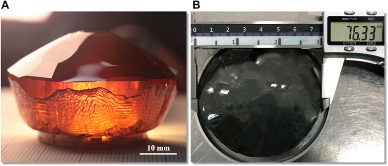
FIGURE 1. (A) as-grown Φ51 mm Al-polar AlN boule (B) as-grown Φ76 mm AlN boule by the homoepitaxial PVT growth technique.
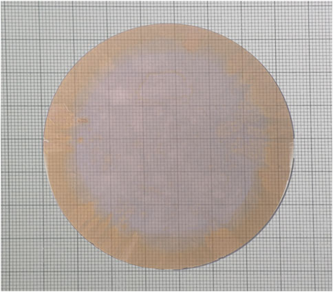
FIGURE 2. Φ75 mm AlN polished sample wafer sliced from the Φ76 mm AlN boule.
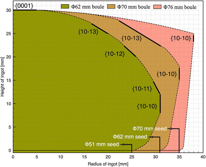
FIGURE 3. Schematic diagram of the AlN crystal shape evolution and growth habit with different diameters.
Typically, the AlN growth temperature during the homoepitaxial PVT growth process is 2,050°C–2,320°C (Hartmann et al., 2008; Hartmann et al., 2014), and the temperature profile near the crystal growth interface is of particular importance to the large-sized AlN lateral expansion growth. Accordingly, the temperature distribution and thermal gradient in the growth chamber mounted with AlN seeds of different sizes (Φ51, Φ62, and Φ70 mm) under the same conditions were calculated using FEMAG and in-house FEMAG codes, as shown in Figure 4. The temperatures at the center of the seed and the top surface of the source were set to 2523.15 and 2543.15 K, respectively, for the heat transfer calculation. The distributions of the temperature (left) and radial thermal gradients (right) are shown in Figure 4. It can be observed that both the maximum temperature and radial thermal gradient occur at the edge of the seed and gradually increase with increasing seed diameter. Further investigation showed that the radial thermal gradient at the edge of the seed increased from .78 to 1.20 K/mm for the seeds with sizes of 51 and 70 mm, respectively. Although a large radial thermal gradient is beneficial for lateral crystal size expansion, an excessively large gradient can cause stress and additional defects to deteriorate the crystal structural quality, such as low-angle grain boundaries (LAGBs), basal plane dislocations (BPDs) and threading dislocations (TDs) or even cracking.
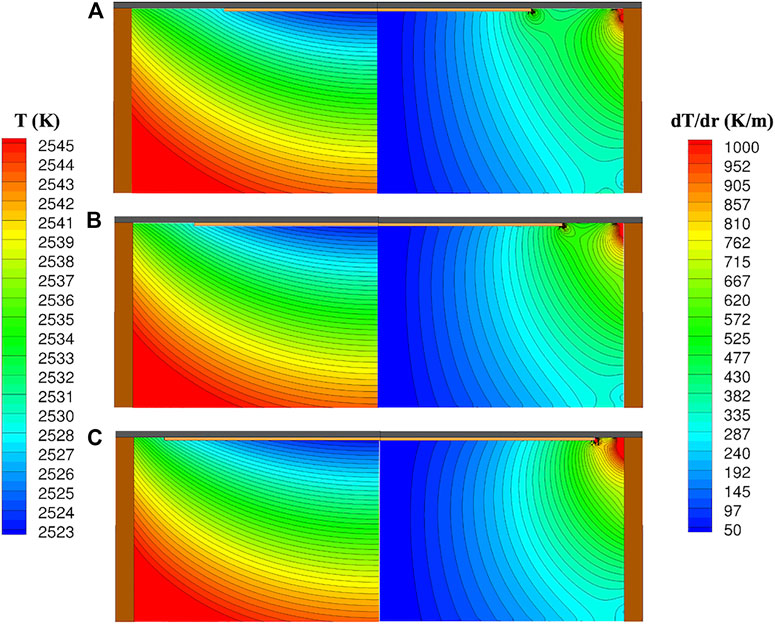
FIGURE 4. Temperature distribution (left) and thermal gradient (right) in the growth chamber mounted with AlN seeds of different sizes: (A) Φ51, (B) Φ62, and (C) Φ70 mm, calculated by FEMAG and in-house FEM codes.
The crystal structure quality was evaluated using the HRXRD ω-rocking curves recorded for the (0002) and (10–12) reflections (as shown in Figure 5). The results were obtained from the central position of each sample sliced from the Φ51, Φ62, and Φ76 mm sc-AlN boules. It was observed that both the full widths at half maximum (FWHMs) of the (0002) and (10–12) reflections increased with the lateral expansion of the crystal diameter. The FWHMs of the (0002) and (10–12) reflections of the Φ76 mm boule were 176 and 109 arcsec, respectively. These results indicate that a slight quality deterioration was observed when the crystal diameter was expanded from Φ51 to Φ76 mm, which could be attributed to various defects such as BPDs, TDs and LAGBs in the crystals because of the non-uniformity of the thermal gradient at the growing crystal interface.
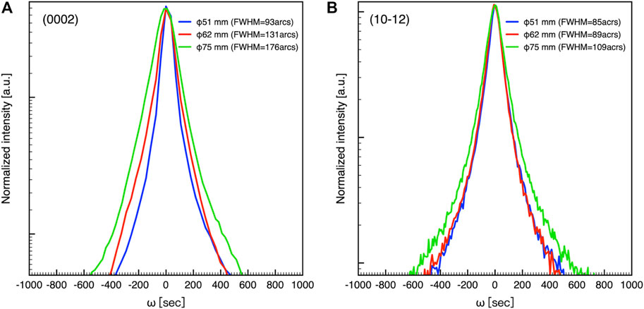
FIGURE 5. Comparison of HRXRD rocking curves of the Φ51, Φ62, and Φ75 mm AlN substrates: (A) symmetric (0002) and (B) asymmetric (10–12) reflections.
To further study the structure defects in the sc-AlN boules, preferential wet chemical etching using eutectic KOH/NaOH solution was conducted for 5 min at 360°C for defect delineation on the Al-polar surface of the polished substrates. The Al-polar surface morphologies and etch pit densities (EPDs) of the etched AlN substrates were investigated using optical microscopy (OM) at 600x. As shown in Figures 6A–C represent the central regions, while Figures 6D–F represent the lateral expansion regions of the Φ51, Φ62, and Φ75 mm substrates, respectively. It can be observed that the EPDs in both the center and lateral expansion regions increased with increasing substrate diameter, which is consistent with the FWHM results obtained by HRXRD. Generally, the EPDs in the peripheral regions for each substrate are higher than those in the central regions because of the higher thermal stress caused by the larger radial thermal gradient during the crystal growth process. Notably, the EPDs in the Φ75 mm substrate was less than 3.0 × 105 cm−2 and etch-pit arrays were rarely observed, indicating that the LAGBs are well suppressed near the substrate periphery.
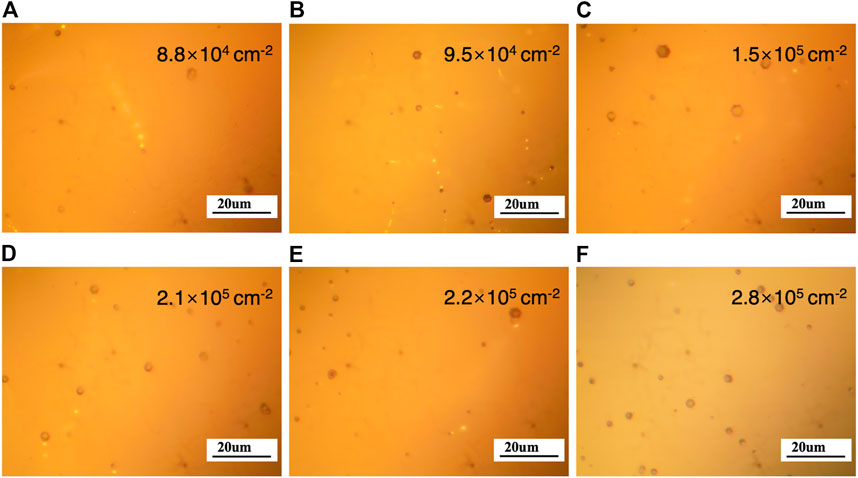
FIGURE 6. Optical micrographs of the (A, D) Φ51, (B, E) Φ62, and (C, F) Φ75 mm substrates after preferential wet chemical etching in eutectic KOH/NaOH solution at 360°C for 5 min.
Deep-UV (DUV) transmission is another key issue in AlN-based optoelectronics. Bulk sc-AlN boules grown by the PVT process generally exhibit UV absorption bands due to the incorporation of carbon and oxygen impurities (Hartman et al., 2014). In the UV disinfection process, the germicidal effect of radiation is most evident in the UV range of 260–280 nm (Hartmann et al., 2016; Tsao et al., 2018; Yu et al., 2021). Figure 7 shows the absorption coefficients (ACs) for the Φ75 mm sample (730 µm thickness after CMP process) in the wavelengths of 200–1,000 nm measured by Perkin–Elmer UV–vis–NIR spectrometer. Two substrate positions (center and edge positions) were analyzed, and all the substrates exhibited ACs of 18–26 cm−1 in the DUV range (240–280 nm), although the Φ76 mm boule showed dark-brown coloration when observed by the naked eye. A below-bandgap absorption band was also observed at approximately 2.8 eV. This absorption band, which has been previously reported in PVT-grown AlN by Bickermann et al. (2010), is responsible for the yellowish coloration of AlN and is believed to be caused by a transition of VAl to ON.
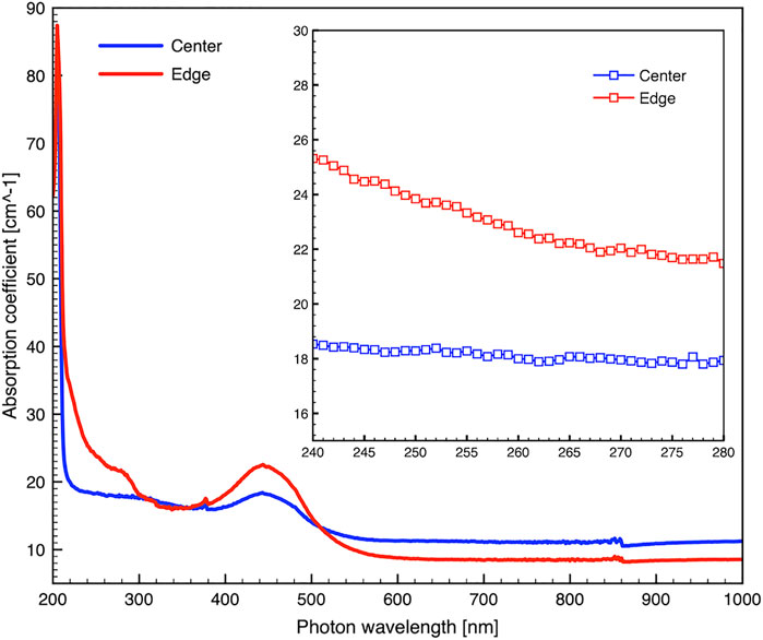
FIGURE 7. Absorption spectra of the center and edge positions of the Φ75 mm sample substrate.
Al-polar sc-AlN boules up to Φ76 mm were prepared using a homoepitaxial growth technique using the PVT method. The evolution of the bbbb shape and growth habit from Φ51 to Φ76 mm was investigated. The symmetric and asymmetric rocking curves obtained by HRXRD showed FWHM values of 176 and 109 arcsec, respectively. The average EPD evaluated by preferential chemical etching was less than 3.0 × 105 cm−2 in the Φ75 mm AlN substrate. The optical transmission spectra revealed that all the substrates exhibited excellent deep-UV transparency with ACs of 18–26 cm−1 in the UV range of 240–280 nm. The characterization results showed that the AlN substrates exhibited good crystallinity and excellent UV transparency, although slight quality deterioration was observed when the crystal size was expanded from Φ51 to Φ76 mm, while the deep-UV transparency remained very similar to that of the AlN seeds. The Φ76 mm sc-AlN boules demonstrated in this study are an important milestone towards achieving Φ100 mm (4-inch) AlN, which are essential for the rapid commercialization of DUV optoelectronics and UWBG electronics.
The original contributions presented in the study are included in the article/Supplementary Material, further inquiries can be directed to the corresponding author.
QW and LW contributed to the design of this research and analyzed and discussed the results of this research. DL, JH, and ZZ contributed to the methodology and performance of the experiments. XS and DL contributed to characterization and analysis of material properties. QW, DL, ZZ, and LW reviewed, edited, and prepared the final draft of this manuscript.
The authors cordially acknowledge financial support from the National Key R&D Program of China (Grant No. 2022YFB3605302), National Natural Science Foundation of China (Grant Nos. 61874071, 61725403, 61827813, and 62121005) and the Key Research and Development Program of Zhejiang Province (2020C01145).
The authors are very grateful for the support of the above project funds.
Authors QW, DL, JH, and LW were employed by Ultratrend Technologies Co., Ltd. and ZZ Sinoma Synthetic Crystals Co., Ltd.
The remaining authors declare that the research was conducted in the absence of any commercial or financial relationships that could be construed as a potential conflict of interest.
All claims expressed in this article are solely those of the authors and do not necessarily represent those of their affiliated organizations, or those of the publisher, the editors and the reviewers. Any product that may be evaluated in this article, or claim that may be made by its manufacturer, is not guaranteed or endorsed by the publisher.
The Supplementary Material for this article can be found online at: https://www.frontiersin.org/articles/10.3389/fmats.2022.1128468/full#supplementary-material
Ambacher, O. (1998). Growth and applications of group III-nitrides. J. Phys. D. Appl. Phys. 31, 2653–2710. doi:10.1088/0022-3727/31/20/001
Bickermann, M., Epelbaum, B. M., Filip, O., Heimann, P., Fenberg, M., Nagata, S., et al. (2010). Deep-UV transparent bulk single-crystalline AlN substrates. Phys. Status Solidi 7, 1743–1745. doi:10.1002/pssc.200983422
Bockowski, M. (2001). Growth and doping of GaN and AlN single crystals under high nitrogen pressure. Cryst. Res. Technol. 36, 771–787. doi:10.1002/1521-4079(200110)36:8/10<771:aid-crat771>3.0.co;2-j
Bondokov, R. T., Mueller, S. G., Morgan, K. E., Slack, G. A., Schujman, S., Wood, M. C., et al. (2008). Large-area AlN substrates for electronic applications: An industrial perspective. J. Cryst. Growth. 310, 4020–4026. doi:10.1016/j.jcrysgro.2008.06.032
Freitas, J. A. (2010). Properties of the state of the art of bulk III-V nitride substrates and homoepitaxial layers. J. Phys. D. Appl. Phys. 43, 073001. doi:10.1088/0022-3727/43/7/073001
Fu, D. Y., Lei, D., Li, Z., Zhang, G., Huang, J. L., Sun, X. J., et al. (2022). Toward Φ56 mm Al-polar AlN single crystals grown by the homoepitaxial PVT method. Cryst. Growth Des. 22, 3462–3470. doi:10.1021/acs.cgd.2c00240
Fu, D. Y., Wang, Q. K., Zhang, G., Li, Z., Huang, J. L., Wang, J., et al. (2021). Influences of powder source porosity on mass transport during AlN crystal growth using physical vapor transport method. Crystals 11, 1436. doi:10.3390/cryst11111436
Fu, D. Y., Wang, Q. K., Zhang, G., Zhu, R. Z., Liu, H., Li, Z., et al. (2020). Modelling and simulation of oxygen transport during AlN crystal growth by the PVT method. J. Cryst. Growth. 551, 125902. doi:10.1016/j.jcrysgro.2020.125902
Hartmann, C., Dittmar, A., Wollweber, J., and Bickermann, M. (2014). Bulk AlN growth by physical vapour transport. Semicond. Sci. Technol. 29, 084002. doi:10.1088/0268-1242/29/8/084002
Hartmann, C., Wollweber, J., Seitz, C., Albrecht, M., and Fornari, R. (2008). Homoepitaxial seeding and growth of bulk AlN by sublimation. J. Cryst. Growth. 310, 930–934. doi:10.1016/j.jcrysgro.2007.11.136
Hartmann, C., Wollweber, J., Sintonen, S., Dittmar, A., Kirste, L., Kollowa, S., et al. (2016). Preparation of deep UV transparent AlN substrates with high structural perfection for optoelectronic devices. CrystEngComm 18, 3488–3497. doi:10.1039/C6CE00622A
Kamei, K., Shirai, Y., Tanaka, T., Okada, N., Yauchi, A., and Amano, H. (2007). Solution growth of AlN single crystal using Cu solvent under atmospheric pressure nitrogen. Phys. Status Solidi C 4, 2211–2214. doi:10.1002/pssc.200674718
Kangawa, Y., Toki, R., Yayama, T., Epelbaum, B. M., and Kakimoto, K. (2011). Novel solution growth method of bulk AlN using Al and Li3N solid sources. Appl. Phys. Express. 4, 095501. doi:10.1143/APEX.4.095501
Katagiri, Y., Kishino, S., Okuura, K., Miyake, H., and Hiramatu, K. (2009). Low-pressure HVPE growth of crack-free thick AlN on a trenchpatterned AlN template. J. Cryst. Growth. 311, 2831–2833. doi:10.1016/j.jcrysgro.2009.01.022
Kumagai, Y., Tajima, J., Ishizuki, M., Nagashima, T., Murakami, H., Takada, K., et al. (2008). Self-separation of a thick AlN layer from a sapphire substrate via interfacial voids formed by the decomposition of sapphire. Appl. Phys. Express. 1, 045003. doi:10.1143/APEX.1.045003
Mueller, S. G., Bondokov, R. T., Morgan, K. E., Slack, G. A., Schujman, S. B., Grandusky, J., et al. (2009). The progress of AlN bulk growth and epitaxy for electronic applications. Phys. Status Solidi A 206, 1153–1159. doi:10.1002/pssa.200880758
Schujman, S. B., Schowalter, L. J., Bondokov, R. T., Morgan, K. E., Liu, W., Smart, J. A., et al. (2008). Structural and surface characterization of large diameter, crystalline AlN substrates for device fabrication. J. Cryst. Growth. 310, 887–890. doi:10.1016/j.jcrysgro.2007.11.134
Slack, G. A., and McNelly, T. F. (1976). Growth of high purity AlN crystals. J. Cryst. Growth. 34, 263–279. doi:10.1016/0022-0248(76)90139-1
Taniyasu, Y., Kasu, M., and Makimoto, T. (2006). An aluminium nitride light-emitting diode with a wavelength of 210 nanometres. Nature 441, 325–328. doi:10.1038/nature04760
Tsao, J. Y., Chowdhury, S., Hollis, M. A., Jena, D., Johnson, N. M., Jones, K. A., et al. (2018). Ultrawide-bandgap semiconductors: Research opportunities and challenges. Adv. Electron. Mat. 4, 1600501. doi:10.1002/aelm.201600501
Wang, Q. K., Huang, J. L., Fu, D. Y., He, G. D., Lei, D., and Wu, L. (2019). Influence of crucible shape on mass transport in AlN crystal growth by physical vapor transport process. J. Cryst. Growth. 515, 21–25. doi:10.1016/j.jcrysgro.2019.02.059
Wang, Q. K., Huang, J. L., Wang, Z. H., He, G. D., Lei, D., Gong, J. C., et al. (2018). Anisotropic three-dimensional thermal stress modeling and simulation of homoepitaxial AlN single crystal growth by the physical vapor transport method. Cryst. Growth Des. 18, 2998–3007. doi:10.1021/acs.cgd.8b00118
Wang, Q. K., Lei, D., He, G. D., Gong, J., Huang, J. L., and Wu, L. (2019). Characterization of 60 mm AlN single crystal wafers grown by the physical vapor transport method. Phys. Status Solidi A 216, 1970052. doi:10.1002/pssa.201970052
Wang, Q. K., Zhao, Y. T., Huang, J. L., Fu, D. Y., He, G. D., and Wu, L. (2019). Optimization of total resolved shear stress in AlN single crystals homoepitaxially grown by physical vapor transport method. J. Cryst. Growth. 519, 14–19. doi:10.1016/j.jcrysgro.2019.04.032
Wang, Z. H., Deng, X. L., Cao, K., Wang, J., and Wu, L. (2017). Hotzone design and optimization for 2-in. AlN PVT growth process through global heat transfer modeling and simulations. J. Cryst. Growth. 474, 76–80. doi:10.1016/j.jcrysgro.2016.12.064
Yu, R. X., Liu, G. X., Wang, G. D., Chen, C. M., Xu, M. S., Zhou, H., et al. (2021). Ultrawide-bandgap semiconductor AlN crystals: Growth and applications. J. Mat. Chem. C 9, 1852–1873. doi:10.1039/D0TC04182C
Zhang, G., Fu, D. Y., Li, Z., Huang, J. L., Wang, Q. K., Ren, Z. M., et al. (2022). Effects of seed-holder shape on the initial growth of AlN crystals by homoepitaxial PVT method. J. Synth. Cryst. 51, 27–34.
Zhao, Q. Y., Zhu, X. Y., Han, T., Wang, Z. R., Wu, J. J., and Yu, T. J. (2022). Realizing overgrowth in the homo-PVT process for 2 inch AlN single crystals. CrystEngComm 24, 1719–1724. doi:10.1039/D1CE01693H
Zhao, Y. T., Wang, Q. K., Zhang, G., Huang, J. L., Fu, D. Y., and Wu, L. (2021). Comparison of the thermal stress behavior of AlN single crystal growth on AlN and SiC seeds via the physical vapor transport method through three-dimensional numerical modeling and simulation. Cryst. Growth Des. 221, 2653–2662. doi:10.1021/acs.cgd.0c01511
Keywords: aluminum nitride, 3-inch, physical vapor transport, homoepitaxial growth, UV transparency
Citation: Wang Q, Lei D, Huang J, Sun X, Li D, Zhou Z and Wu L (2023) Homoepitaxial growth of 3-inch single crystalline AlN boules by the physical vapor transport process. Front. Mater. 9:1128468. doi: 10.3389/fmats.2022.1128468
Received: 20 December 2022; Accepted: 30 December 2022;
Published: 10 January 2023.
Edited by:
Rong Wang, Zhejiang University, ChinaCopyright © 2023 Wang, Lei, Huang, Sun, Li, Zhou and Wu. This is an open-access article distributed under the terms of the Creative Commons Attribution License (CC BY). The use, distribution or reproduction in other forums is permitted, provided the original author(s) and the copyright owner(s) are credited and that the original publication in this journal is cited, in accordance with accepted academic practice. No use, distribution or reproduction is permitted which does not comply with these terms.
*Correspondence: Liang Wu, amFzb24ud3VAdXRyZW5kdGVjaC5jb20=
Disclaimer: All claims expressed in this article are solely those of the authors and do not necessarily represent those of their affiliated organizations, or those of the publisher, the editors and the reviewers. Any product that may be evaluated in this article or claim that may be made by its manufacturer is not guaranteed or endorsed by the publisher.
Research integrity at Frontiers
Learn more about the work of our research integrity team to safeguard the quality of each article we publish.