 Yajie Dai1
 Shouxin Zhao2
 Hui Han1
 Yafei Yan1Wenhui Liu1Hua Zhu1Liang Li1Xi Tang1Yang Li2
 Hui Li1*Changjin Zhang1,3
- 1Institute of Physical Science and Information Technology and Information Materials and Intelligent Sensing Laboratory of Anhui Province, Anhui University, Hefei, China
- 2School of Materials Science and Engineering, Harbin Institute of Technology, Harbin, China
- 3High Magnetic Field Laboratory of Anhui Province, Chinese Academy of Sciences, Hefei, China
The controlled growth of indium selenides has attracted considerable research interests in condensed matter physics and materials science yet remains a challenge due to the complexity of the indium–selenium phase diagram. Here, we demonstrate the successful growth of indium selenides in a controllable manner using the high-pressure and high-temperature growth technique. The γ-InSe and α-In2Se3 crystals with completely different stoichiometries and stacking manner of atomic layers have been controlled grown by subtle tuning growth temperature, duration time, and growth pressure. The as-grown γ-InSe crystal features a semiconducting property with a prominent photoluminescence peak of ∼1.23 eV, while the α-In2Se3 crystal is ferroelectric. Our findings could lead to a surge of interest in the development of the controlled growth of high-quality van der Waal crystals using the high-pressure and high-temperature growth technique and will open perspectives for further investigation of fascinating properties and potential practical application of van der Waal crystals.
Introduction
Indium selenides (InxSey) are group III–VI semiconductors with kinds of In and Se stoichiometries and several structural modifications, for example, InSe with β, ε, and γ phases, and In2Se3 with α, β, γ, and σ phases (Butler et al., 2013; Bandurin et al., 2017; Balakrishnan et al., 2018). The rich tapestry of stoichiometries and structures of indium selenides makes them the treasure trove for fascinating properties with prospects in both frontier fundamental research and electronic device design, such as exotic ferroelectricity in α-In2Se3, ultrahigh electron mobility (>104 cm2 V−1 s−1 at low temperature) of γ-InSe, and excellent photoresponsivity in β-InSe (Lei et al., 2014; Milutinović et al., 2016; Ding et al., 2017; Tang et al., 2019; Guo et al., 2020; Li et al., 2020; Ding et al., 2021).
Among them, γ-InSe and α-In2Se3 are two promising materials that have achieved considerable attention. Both γ-InSe and α-In2Se3 are layered structures with the intralayer being covalent bonded and the interlayers being interacted by van der Waals force, as shown in the schematic drawing of crystal structures in Figure 1. The γ-InSe consists of quadruple Se-In-In-Se layers in the rhombohedral stacking behavior (Figure 1A), while the α-In2Se3 is composed of Se-In-Se-In-Se quintuple layers arranged in a rhombohedral (R3m) crystal structure (Figure 1B) (Butler et al., 2013; Bandurin et al., 2017; Balakrishnan et al., 2018; Tang et al., 2019). Such different stacking behaviors of In and Se atoms result in the γ-InSe and α-In2Se3 featuring distinct physical properties, which offers a new frontier of investigation on the relationship between the structures and properties. However, it is still a challenge to grow γ-InSe and α-In2Se3 in a controllable way because the energy difference between abundant structures of indium selenides is quite small.
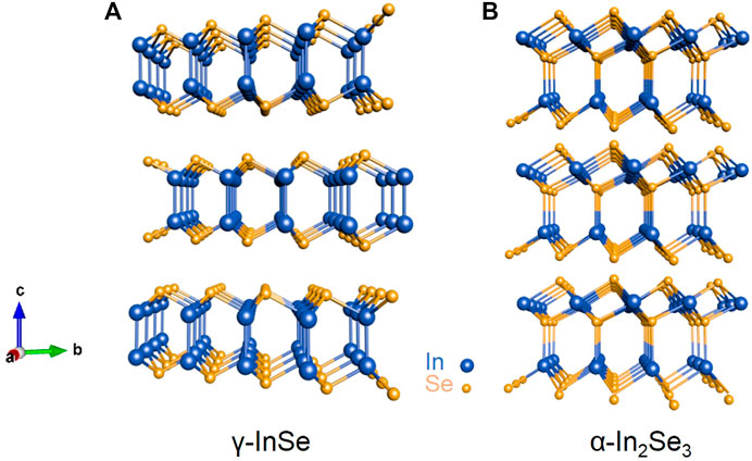
FIGURE 1. Schematic rhombohedral crystal structure of γ-InSe consisting of quadruple Se-In-In-Se layers (A) and α-In2Se3 composed of Se-In-Se-In-Se quintuple layers (B) in 3D form.
Several approaches have been attempted to control grow γ-InSe and α-In2Se3, including chemical vapor deposition (CVD), chemical vapor transport (CVT), physical vapor deposition (PVD), pulse laser deposition (PLD), and the Bridgman method (Ishii, 1988; Zhou et al., 2016; Yang et al., 2017; Hu et al., 2018). Although substantial success has been achieved, the controlled growth of γ-InSe and α-In2Se3 still suffers from nonuniformity and time-consuming issues. Thus, the development of novel growth techniques is highly desirable. Recently, a few studies reported the utilization of the high-pressure and high-temperature (HPHT) growth method to grow the two-dimensional layered single crystals (Watanabe and Taniguchi, 2019). The high temperature and high pressure facilitate the crystallization and growth of crystals remarkably, which has provided an alternative and effective way toward the controlled growth of single crystals. However, the controlled growth of indium selenides using the HPHT technique has not been investigated. In this work, we systematically investigate the controlled growth of γ-InSe and α-In2Se3 using the HPHT growth technique by subtly adjusting the growth temperature, duration time, and the ratios of precursors. The photoluminescence (PL) of the as-grown γ-InSe and the ferroelectricity of the α-In2Se3 are further investigated.
Results and Discussion
The controlled growth of InxSey crystals with different stoichiometries was realized by the HPHT growth technique. Figure 2 summarizes the controlled growth of InxSey crystals with different stoichiometries by subtle tuning growth temperature, duration time, and the ratios of precursors (precursor In/Se ratio) with the growth pressure of 0.76 GPa. As shown in Figure 2A, the crystalline InxSey with mixed stoichiometries of 2:3 and 1:1 is obtained at 250°C with duration time of 20 min and precursor In/Se ratio of 2.1:3. Such a mixing behavior might be due to the nonuniform reaction under the relatively low growth temperature of 250°C, which is very close to the melting points of In (156.6°C) and Se (221°C). Importantly, if we increase the reaction temperature, the mixing behavior could be completely eliminated. As can be seen from Figure 2A, crystalline InSe with a stoichiometry of 1:1 could be obtained at growth temperature of 300°C and 350°C, while the crystalline In2Se3 with a stoichiometry of 2:3 is eventually achieved as the growth temperature further increases to 400°C with other growth conditions unchanged. The present results are in principle consistent with the provisional equilibrium In-Se binary phase diagram (Lu et al., 1999), in which In2Se3 crystals are preferred to be formed at relatively high temperatures.
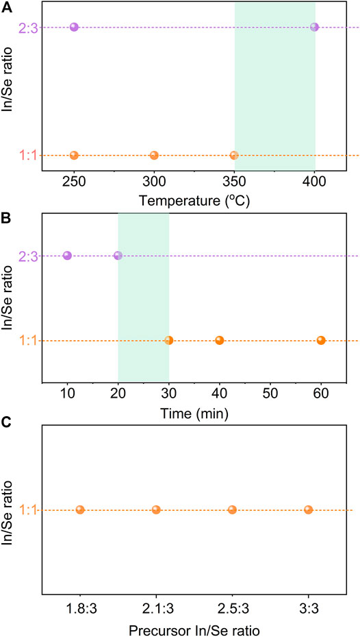
FIGURE 2. Controlled growth of indium selenides using HPHT growth technique under 0.76 GPa. The growth temperature (A), growth duration time (B), and precursor ratio (C) dependence of the stoichiometry of final grown crystals. The shadow rectangle in (A) and (B) indicates the transition region. HPHT, high pressure and high temperature.
We further demonstrate that the stoichiometry of the obtained crystals could be effectively modulated by the growth duration time. As shown in Figure 2B, the stoichiometry of the obtained crystals changes from 2:3 (i.e., In2Se3) to 1:1 (i.e., InSe) with the growth duration time increasing from 10 to 30 min under 0.76 GPa and 400°C with precursor In/Se ratio of 2.1:3, indicating that the longer growth duration time is beneficial for the growth of InSe crystals. Further increasing duration time to 60 min does not change the stoichiometry of the obtained crystals.
In contrast to the growth temperature and duration time, the In/Se ratios of the precursors have no influence on the stoichiometry of the resultant crystals. The InSe crystals with a stoichiometry of 1:1 are obtained even with the precursor In/Se ratio changes in a wide range from 1.8:3 to 3:3 under the growth condition of 0.76 GPa, 400°C, and duration time of 30 min (Figure 2C).
We perform a systematical investigation on the growth of InxSey crystal with a controlled stoichiometry by adjusting the growth conditions, including growth pressure, duration time, and precursor ratios. As summarized in Supplementary Table S1, no bulk crystalline products were obtained under growth pressure above 2 GPa with various kinds of growth temperatures, growth duration time, and precursor In/Se ratio. This fact suggests that the high pressure above 2 GPa is not favorable in the growth of InxSey crystals.
Figure 3 shows the optical images and scanning electron microscopy (SEM) images of the obtained crystals grown under 0.76 GPa and 400°C with In/Se precursor ratio of 2.1:3 for 30 and 10 min. The stoichiometry of the crystals is determined to be InSe (Figure 3A) and In2Se3 (Figure 3B) by the energy-dispersive X-ray spectroscopy (EDS) analysis, as shown in Supplementary Figure S1. The as-grown crystals are shiny with large sizes of about 5 × 1.6 mm for InSe (Figure 3A) and of about 1.7 × 1.3 mm for In2Se3 (Figure 3B). In addition, the resultant crystals exhibit clearly layered structures, as shown in the SEM images in Figures 3C,D.
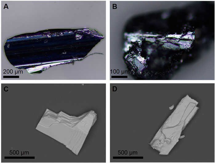
FIGURE 3. Optical images of as-grown InSe crystal (A) and In2Se3 crystal (B). SEM image of InSe crystal (C) and In2Se3 crystal (D) exfoliated on SiO2 substrate. SEM, scanning electron microscopy.
Raman spectra were utilized to identify the phases of the InSe and In2Se3 crystals, as indicated in Figure 4. Four Raman modes, namely,
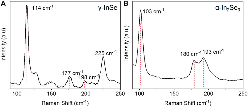
FIGURE 4. Micro-Raman spectra of γ-InSe flake (A) and α-In2Se3 flake (B) with excitation laser wavelength of 532 nm.
The crystal structures of the single crystals are further investigated by transmission electron microscopy (TEM). The thin γ-InSe and α-In2Se3 flakes were transferred on Cu grids by mechanical exfoliation and standard wet transfer method. Figure 5A shows the morphology of γ-InSe flakes. The selected area electron diffraction pattern (Figure 5B) measured in the marked area (red ellipse in Figure 5A) shows a six-fold symmetry, which suggests that the InSe crystals are of hexagonal structure. The high-resolution TEM image of the InSe flake clearly shows the hexagonal structure with the angle between the well-recognized a and b axes at 120o (Figure 5C). The lattice constant is determined to be about 0.4 nm, which is consistent with the lattice spacing of layered γ-InSe (a = b = 4.005 Å, c = 24.96 Å) (Chen et al., 2015). The same TEM investigations were also carried out on α-In2Se3 flakes, as shown in Figures 5D–F. The lattice constant is measured to be about 0.35 nm, which corresponds to d-spacing (100) lattice planes of α-In2Se3 (Ho et al., 2013; Zhou et al., 2015; Feng et al., 2016; Zhou et al., 2017; Tang et al., 2019).
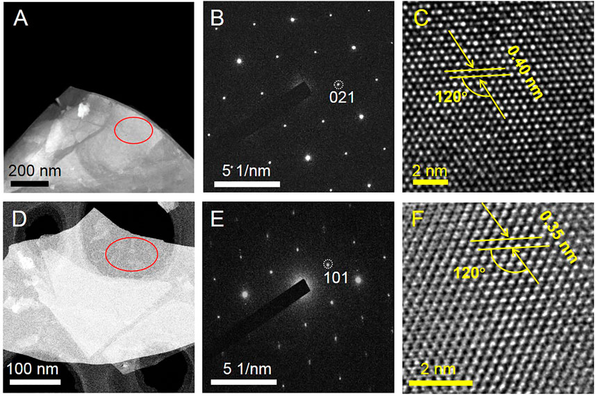
FIGURE 5. (A) TEM image of γ-InSe flake. (B) SAED pattern and (C) HR-TEM image of γ-InSe flake collected in the marked area in (A). (D) TEM image of α-In2Se3 flake. (E) SAED pattern and (F) HR-TEM image of α-In2Se3 flake collected in the marked area in (D). TEM, transmission electron microscopy; SAED, selected area electron diffraction; HR-TEM, high-resolution TEM.
Figure 6 shows the PL spectra of the γ-InSe flakes exfoliated from the as-grown crystals. A prominent peak at ∼1.23 eV is observed for ∼22-nm γ-InSe (Figure 6A). The thickness of γ-InSe flake is determined by the atomic force measurement, as shown in Supplementary Figure S2. By increasing the excitation laser power, the PL peak intensity increases. The excitation power dependence of the PL peak intensity follows the power law,
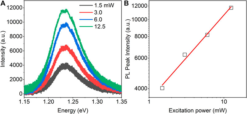
FIGURE 6. (A) Photoluminescence (PL) spectra of the γ-InSe flake of about 22 nm at different incident laser power indicated. (B) Log–log plot of PL intensity as a function of the excitation power. The solid red line is the linear fitting curve with power-law index of ∼0.5.
The piezoelectricity of the as-grown α-In2Se3 has been further investigated by the piezoresponse force microscopy (PFM) measurements. Figure 7 shows the out-of-plane PFM amplitude (Figure 7A) and phase image (Figure 7B). The high and low amplitudes are clearly observed in the inner square and outer square, respectively, which corresponds to the opposite polarization states after writing with +7 V and −5 V, respectively. In addition, the domain wall between the oppositely polarized region is clear and does not coincide with the edges of the samples, which excludes the contribution of other artifact effects.
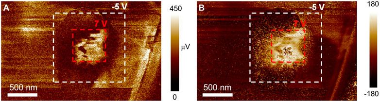
FIGURE 7. The out-of-plane PFM amplitude (A) and phase (B) of as-grown α-In2Se3 flake exfoliated on SiO2 substrate. The red and white dashed areas are polarized using different driving voltages of +7 V and −5 V, respectively. PFM, piezoresponse force microscopy.
Conclusion
The controlled growth of indium selenide crystals was achieved successfully using the HPHT growth technique. The stoichiometry and structure of the indium selenides were well controlled by tuning the growth temperature and duration time at specific growth pressure of 0.76 GPa. The relatively low growth temperature and long duration time are beneficial for the growth of γ-InSe. On the contrary, α-In2Se3 crystals could be easily obtained at relatively high growth temperature and short growth duration time. Moreover, diverse physical properties were observed in the resultant crystals; i.e., γ-InSe shows a prominent PL peak at ∼1.23 eV, and α-In2Se3 exhibits evident ferroelectricity, which holds promise for the potential applications in optoelectronics and ferroelectric memory devices. Our findings have provided an alternative strategy for crystals growth in a controlled manner and will stimulate further development of high-quality crystal growth with numerous fascinating physical properties and functional device applications.
Methods
Characterization
Structural investigations and stoichiometry analyses of as-grown crystals were determined by EDS analysis through a field-emission SEM (JEOL-7100F, JEOL Ltd, Tokyo, Japan) at room temperature. The high-resolution images are measured by TEMs (JEM 2010; JEOL) with an acceleration voltage of 200 kV. The PL spectra were collected on micro-Raman/PL system (InVia, Renishaw, Wotton-under-Edge, UK) using an argon green laser at 514 nm. PFM measurements were performed in ambient conditions by using scanning probe microscopies (Bruker Dimension Icon-PT, Kontich, Belgium). Co/Cr tips (MESP, Bruker) were used for PFM measurements. An ac driving voltage of 0.5–1 V at a near resonance frequency of 280–400 kHz was applied to collect the PFM domain images (PFM phase and amplitude).
Data Availability Statement
The raw data supporting the conclusion of this article will be made available by the authors, without undue reservation.
Author Contributions
HL conceived the project. YD grew and characterized the crystals with support from HH, YL, WL, HZ, XT, SZ and YL. All authors contributed to the article and approved the submitted version.
Funding
This work was supported in part by the National Natural Science Foundation of China under Grant Nos. 11904001 and 51902069, the Joint Funds of the National Natural Science Foundation of China and the Chinese Academy of Sciences Large-Scale Scientific Facility under Grant No. U1932156, the Natural Science Foundation of Anhui Province under Grant No. 2008085QA29, and the Project of Science and Technology on Reliability Physics and Application Technology of Electronic Component Laboratory under Grant No. 61428060101.
Conflict of Interest
The authors declare that the research was conducted in the absence of any commercial or financial relationships that could be construed as a potential conflict of interest.
Publisher’s Note
All claims expressed in this article are solely those of the authors and do not necessarily represent those of their affiliated organizations, or those of the publisher, the editors, and the reviewers. Any product that may be evaluated in this article, or claim that may be made by its manufacturer, is not guaranteed or endorsed by the publisher.
Supplementary Material
The Supplementary Material for this article can be found online at: https://www.frontiersin.org/articles/10.3389/fmats.2021.816821/full#supplementary-material
References
Balakrishnan, N., Steer, E. D., Smith, E. F., Kudrynskyi, Z. R., Kovalyuk, Z. D., Eaves, L., et al. (2018). Epitaxial Growth of γ -InSe and α , β , and γ -In 2 Se 3 on ε -GaSe. 2d Mater. 5, 035026. doi:10.1088/2053-1583/aac479
Bandurin, D. A., Tyurnina, A. V., Yu, G. L., Mishchenko, A., Zólyomi, V., Morozov, S. V., et al. (2017). High Electron Mobility, Quantum Hall Effect and Anomalous Optical Response in Atomically Thin InSe. Nat. Nanotech 12, 223–227. doi:10.1038/nnano.2016.242
Brener, I., Olszakier, M., Cohen, E., Ehrenfreund, E., Ron, A., and Pfeiffer, L. (1992). Particle Localization and Phonon Sidebands in GaAs/AlxGa1−xAs Multiple Quantum wells. Phys. Rev. B 46, 7927–7930. doi:10.1103/physrevb.46.7927
Butler, S. Z., Hollen, S. M., Cao, L., Cui, Y., Gupta, J. A., Gutiérrez, H. R., et al. (2013). Progress, Challenges, and Opportunities in Two-Dimensional Materials beyond Graphene. ACS Nano. 7, 2898–2926. doi:10.1021/nn400280c
Chen, Z., Biscaras, J., and Shukla, A. (2015). A High Performance Graphene/few-Layer InSe Photo-Detector. Nanoscale 7, 5981–5986. doi:10.1039/c5nr00400d
Ding, J., Shao, D. F., Li, M., Wen, L. W., and Tsymbal, E. Y. (2021). Two-dimensional Antiferroelectric Tunnel junction. Phys. Rev. Lett. 126, 057601. doi:10.1103/PhysRevLett.126.057601
Ding, W., Zhu, J., Wang, Z., Gao, Y., Xiao, D., Gu, Y., et al. (2017). Prediction of intrinsic two-dimensional ferroelectrics in In2Se3 and other III2-VI3 van der Waals materials. Nat. Commun. 8, 14956. doi:10.1038/ncomms14956
Feng, W., Zheng, W., Gao, F., Chen, X., Liu, G., Hasan, T., et al. (2016). Sensitive Electronic-Skin Strain Sensor Array Based on the Patterned Two-Dimensional α-In2Se3. Chem. Mater. 28, 4278–4283. doi:10.1021/acs.chemmater.6b01073
Guo, H., Zhang, Z., Huang, B., Wang, X., Niu, H., Guo, Y., et al. (2020). Theoretical study on the photocatalytic properties of 2D InX(X = S, Se)/transition metal disulfide (MoS2 and WS2) van der Waals heterostructures. Nanoscale 12, 20025–20032. doi:10.1039/d0nr04725b
Ho, C.-H., Lin, C.-H., Wang, Y.-P., Chen, Y.-C., Chen, S.-H., and Huang, Y.-S. (2013). Surface Oxide Effect on Optical Sensing and Photoelectric Conversion of α-In2Se3 Hexagonal Microplates. ACS Appl. Mater. Inter. 5, 2269–2277. doi:10.1021/am400128e
Hu, Y., Feng, W., Dai, M., Yang, H., Chen, X., Liu, G., et al. (2018). Temperature-dependent Growth of Few Layer β-InSe and α-In2Se3 Single Crystals for Optoelectronic Device. Semicond. Sci. Technol. 33, 125002. doi:10.1088/1361-6641/aae629
Ishii, T. (1988). High Quality Single crystal Growth of Layered InSe Semiconductor by bridgman Technique. J. Cryst. Growth 89, 459–462. doi:10.1016/0022-0248(88)90206-0
Lei, S., Ge, L., Najmaei, S., George, A., Kappera, R., Lou, J., et al. (2014). Evolution of the Electronic Band Structure and Efficient Photo-Detection in Atomic Layers of InSe. ACS Nano. 8, 1263–1272. doi:10.1021/nn405036u
Lewandowska, R., Bacewicz, R., Filipowicz, J., and Paszkowicz, W. (2001). Raman Scattering in α-In2Se3 Crystals. Mater. Res. Bull. 36, 2577–2583. doi:10.1016/s0025-5408(01)00746-2
Li, Y.-H., Yu, C.-B., Li, Z., Jiang, P., Zhou, X.-Y., Gao, C.-F., et al. (2020). Layer-dependent and Light-Tunable Surface Potential of Two-Dimensional Indium Selenide (InSe) Flakes. Rare Met. 39, 1356–1363. doi:10.1007/s12598-020-01511-4
Lu, K., Sui, M. L., Perepezko, J. H., and Lanning, B. (1999). The Kinetics of Indium/amorphous-Selenium Multilayer Thin Film Reactions. J. Mater. Res. 14, 771–779. doi:10.1557/jmr.1999.0103
Milutinović, A., Lazarević, Z. Z., Jakovljević, M., Hadzić, B., Petrović, M., Petrović, M., et al. (2016). Optical Properties of Layered III-VI Semiconductor γ-InSe: M (M=Mn, Fe, Co, Ni). J. Phys. Chem. Sol. 86, 120–127.
Mudd, G. W., Svatek, S. A., Ren, T., Patanè, A., Makarovsky, O., Eaves, L., et al. (2013). Tuning the Bandgap of Exfoliated InSe Nanosheets by Quantum Confinement. Adv. Mater. 25, 5714–5718. doi:10.1002/adma.201302616
Tang, L., Teng, C., Luo, Y., Khan, U., Pan, H., Cai, Z., et al. (2019). Confined van der Waals Epitaxial Growth of Two-Dimensional Large Single-Crystal In2Se3 for Flexible Broadband Photodetectors. Research 2019, 1–10. doi:10.1155/2019/2763704
Watanabe, K., and Taniguchi, T. (2019). Far-UV Photoluminescence Microscope for Impurity Domain in hexagonal-boron-nitride Single Crystals by High-Pressure, High-Temperature Synthesis. Npj 2d Mater. Appl. 3, 40. doi:10.1038/s41699-019-0124-4
Wu, M., Xie, Q., Wu, Y., Zheng, J., Wang, W., He, L., et al. (2019). Crystal Structure and Optical Performance in Bulk γ-InSe Single Crystals. AIP Adv. 9, 025013. doi:10.1063/1.5086492
Yang, Z., Jie, W., Mak, C.-H., Lin, S., Lin, H., Yang, X., et al. (2017). Wafer-scale Synthesis of High-Quality Semiconducting Two-Dimensional Layered InSe with Broadband Photoresponse. ACS Nano. 11, 4225–4236. doi:10.1021/acsnano.7b01168
Zhou, J., Zeng, Q., Lv, D., Sun, L., Niu, L., Fu, W., et al. (2015). Controlled Synthesis of High-Quality Monolayered α-In2Se3 via Physical Vapor Deposition. Nano. Lett. 15, 6400–6405. doi:10.1021/acs.nanolett.5b01590
Zhou, S., Tao, X., and Gu, Y. (2016). Thickness-Dependent Thermal Conductivity of Suspended Two-Dimensional Single-Crystal In2Se3 Layers Grown by Chemical Vapor Deposition. J. Phys. Chem. C 120, 4753–4758. doi:10.1021/acs.jpcc.5b10905
Keywords: indium selenides, controlled growth, high-pressure and high-temperature, photoluminescence, ferroelectricity
Citation: Dai Y, Zhao S, Han H, Yan Y, Liu W, Zhu H, Li L, Tang X, Li Y, Li H and Zhang C (2022) Controlled Growth of Indium Selenides by High-Pressure and High-Temperature Method. Front. Mater. 8:816821. doi: 10.3389/fmats.2021.816821
Received: 17 November 2021; Accepted: 02 December 2021;
Published: 11 January 2022.
Edited by:
Zhaofu Zhang, University of Cambridge, United KingdomCopyright © 2022 Dai, Zhao, Han, Yan, Liu, Zhu, Li, Tang, Li, Li and Zhang. This is an open-access article distributed under the terms of the Creative Commons Attribution License (CC BY). The use, distribution or reproduction in other forums is permitted, provided the original author(s) and the copyright owner(s) are credited and that the original publication in this journal is cited, in accordance with accepted academic practice. No use, distribution or reproduction is permitted which does not comply with these terms.
*Correspondence: Hui Li, aHVpbGlAYWh1LmVkdS5jbg==