 Xiaojuan Lian1,2
 Jinke Fu1
 Zhixuan Gao1Wang Ren3Xiang Wan1Qingying Ren4Jing Wen5Cihui Yang5
 Xiaoyan Liu1*
 Lei Wang1*
- 1Department of Microelectronics, College of Electrical and Optical Engineering and College of Microelectronics, Nanjing University of Post and Telecommunications, Nanjing, China
- 2National and Local Joint Engineering Laboratory of RF Integration and Micro-Assembly Technology, Nanjing, China
- 3Shanghai Aerospace Electronic Technology Institute, Shanghai, China
- 4Electrical and Electronic Laboratory Center, College of Electrical and Optical Engineering and College of Microelectronics, Nanjing University of Post and Telecommunications, Nanjing, China
- 5School of Information Engineering, Nanchang Hangkong University, Nanchang, China
Phase-change random access memory (PCRAM) is widely regarded as one of the most promising candidates to replace Flash memory as the next generation of non-volatile memories due to its high-speed and low-power consumption characteristics. Recent advent of the blade-type PCRAM with low programming current merit further confirms its prospects. The thermoelectric effects existing inside the PCRAM devices have always been an important factor that determines the phase-transformation kinetics due to a fact that it allows PCRAM to have electric polarity dependent characteristics. However, the potential physics governing the thermoelectric effects for blade-type PCRAM device still remains vague. We establish a three-dimensional (3D) electro-thermal and phase-transformation model to study the influences of thermal boundary resistance (TBR) and device scaling on the thermoelectric effects of the blade-type PCRAM during its “RESET” operation. Our research shows that the presence of TBR significantly improves the electric polarity-dependent characteristics of the blade-type PCRAM, and such polarity-dependent characteristic is found immune to the scaling of the device. It is therefore possible to optimize the thermoelectric effects of the blade-type PCRAM through appropriately tailoring the TBR parameters, thus further lowering resulting power consumption.
Introduction
To make machine think, infer, and behave like human being has always been the ultimate dream of the global scientists. In order to achieve this goal, the current consensus is to build a machine that replicates the complex neural networks of the biological brain (LeCun et al., 2015). Such artificial neural networks (ANNs) were usually constructed from various sophisticated algorithms, and most recently received the utmost attention by virtue of “deep learning” strategy (Han et al., 2021; Jing and Tian, 2021; Patel et al., 2021). Although current ANNs exhibit their fascinating performances particularly in the fields of image and voice recognitions (Wang et al., 2019), they are still facing some formidable drawbacks such as manufacture cost and energy consumption (Bedolla et al., 2021). Most importantly, the software-based ANNs still adopt the well-known von Neumann mode that data storage and processing functionalities are performed by memory and central processing unit (CPU) (Indiveri and Liu, 2015), respectively. This work mechanism obviously deviates from that of the biological brain that has data processing and storage taking place at the same place. To address this issue, considerable research enthusiasm has been switched to the realization of ANNs using hardware devices, particularly in the form of non-volatile memories (NVMs) (Howard et al., 2014; Ni et al., 2019; Oh et al., 2019; Umesh and Mittal, 2019; Choi et al., 2020). NVMs families including ferroelectric random-access memory, magnetic random-access memory, phase-change random access memory (PCRAM), and resistive random-access memory, were initially devised to replace static random-access memory and dynamic random-access memory for future memory devices (Zhang et al., 2020). Triggered by recent progress of semiconductor technologies, several encouraging features such as ultra-high integration density (Chen et al., 2019), ultra-small energy consumption (Gunzel et al., 2021), ultra-fast write/read speed (Zhou et al., 2022), and long data retention (Dongale et al., 2021), have been found on NVMs. These superior traits astonishingly match the biological properties of the brain neurons and synapses. Most importantly, one certain physical state of the NVMs e.g., electric resistance, can be continuously modulated by means of external excitations, which can be harnessed to achieve important functionalities of arithmetic and logic computing (Feldmann et al., 2017; Sebastian et al., 2019; Adam, 2020). This undoubtedly renders NVMs a capability of working in non-von Neumann mode, thus opening a route towards the success of hardware-based ANNs.
As an already commercialized product of NVMs families, PCRAM has attained tremendous interest during last decade, and recent advent of 3D XPoint memory further intensifies the attention on PCRAM from worldwide researchers (Liu and Chen, 2020). The key materials used for PCRAM applications usually comprises chalcogens elements of the periodic table, which are also known as phase-change materials (PCMs). The atomic structures of the PCMs can be rapidly and reversibly switched between a so-called crystalline state with long-range order and a so-called amorphous state with short-range order. To induce amorphization (namely “RESET”), it is necessary to heat the crystalline PCMs above the melting temperature, followed by a rapid cooling. In contrast, crystallization (namely “SET”) is achieved by increasing the temperature inside the amorphous PCMs up to the glass transition point. The most charming feature of PCMs arises from the remarkable difference on the electric resistivity and optical reflectivity between the crystalline and amorphous PCMs. Given this fact, the distinct electrical or optical properties of the PCMs can be implemented to describe the binary codes of “1” and “0,” thus realizing the storage functionality. Owing to this attractive trait, PCMs, particularly represented by Ge2Sb2Te5 alloy (GST), have been commonly adopted for various commercialized phase-change memories such as rewritable digital versatile disc (DVD) (Pieterson et al., 2004), Blu-ray disc (Aoki, 2003), and PCRAM (Kwon et al., 2015). Additionally, their ability to dynamically modulate either the electric resistance or the optical reflectivity renders these devices with an exciting memristive behavior, thereby triggering their new applications including in-memory computing (Noori et al., 2021) and neuromorphic computing (Wang et al., 2017a).
In spite of above progress, the conventional PCRAM device, such as Lance-type architecture (Figure 1A) (Navarro et al., 2013), usually requires large programming current for inducing phase-transformation. This can be accomplished using a cell selector with large size in order to provide adequately high current drivability, which however impairs the scalability of the PCRAM device. This drawback can be substantially mitigated using a so-called blade-type PCRAM structure (Jin et al., 2016), as illustrated in Figure 1B. The comparison between Figures 1A,B clearly indicates that both architectures are composed of a GST layer sandwiched between a top metal electrode and a resistive electrode (namely heater), which are deposited on a bottom metal electrode. The sole difference stems from the observation that the blade-type PCRAM has a blade GST layer and a blade heater, whereas the Lance-type only includes a blade heater. Using double blade shaped layers can obviously reduce the size of the interfacial region and significantly lower the programming current. As a result, the electro-thermal performances of the blade-type PCRAM have recently been under extensive research either experimentally or by simulations (Jin et al., 2016; Wang et al., 2017b; Wen and Wang, 2020). However, the well-known thermoelectric (TE) effects that reportedly plays an important role in determining the phase-transformation kinetics of the Lance-type PCRAM was astonishingly ignored by the previous study (Lee et al., 2012; Faraclas et al., 2014). To solve this issue, we here integrated the TE effects with our previously established electro-thermal model to investigate the potential factors that impact the TE effects on the blade-type PCRAM. Note that here we only take into account the “RESET” operation that is the most commonly used write mode for PCRAM applications. The outcomes are likely to provide a deeper understanding on the physical performances of the blade-type PCRAM, to setup a device design rule, and eventually to optimize the geometrical and material parameters of the blade-type PCRAM.
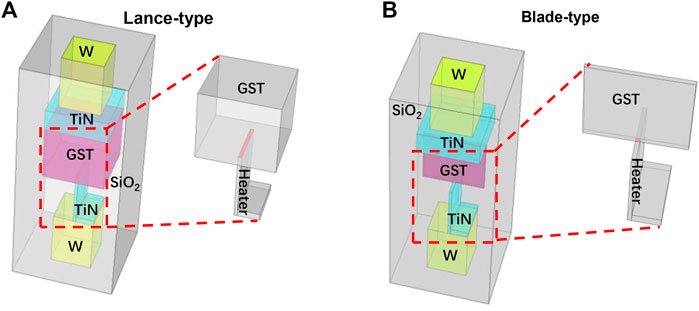
FIGURE 1. Designed PCRAM architecture with (A) Lance-type shape and (B) blade-type shape. Zoom in on the area bounded by red dash clearly exhibits the difference on size of the GST-heater interface between these two structures.
Methods
The geometrical structure of the adopted blade-type PCRAM cell is illustrated in Figure 2A. A 120 nm thick GST layer is sandwiched between a 40 nm thick titanium nitride (TiN) top contactor and a 100 nm thick TiN heater. The top and bottom electrodes are made of two 100 nm thick tungsten (W) layers giving a diameter of 120 nm. The blade contact region at the GST-heater interface is assumed to be a 5 nm ◊5 nm tile. Such cell is entirely encapsulated by a silicon dioxide (SiO2) surroundings that allows for superb electrical and thermal insulation. A newly established electro-thermal and phase-change kinetic model, consisting of the improved versions of current continuity equation, and the heat transfer equation to include the TE effects, is employed here to calculate the phase-transformation extent, giving rise to:
where J, σ, d, Cp, k correspond to current density, electrical conductivity, density, heat capacity, and thermal conductivity of each layered media inside the designed device, respectively; V, E, T indicate the electric potential, electric field, and temperature inside the designed device, respectively. S is the Seebeck coefficient of the GST layer, and its related term, -σ·S∇T, is interpreted as the thermally driven diffusion current that contributes to the TE heat. The TE heat is regarded as the sum of the Thomson heat (QT) that takes place inside the bulk GST and TiN heater, and the Peltier heat (QP) occurring at the GST-heater interface. Adding the TE heat to the Joule heat (QJ) gives rise to the total heat source of the blade type PCRAM, which governs the temperature and phase-transformation distributions inside the GST layer. The crystalline GST region is assumed amorphized once its temperature and cooling rate exceed 620°C and 37°C/ns (Wright et al., 2006), respectively. Once amorphization is formed, its electrical and thermal conductivities are correspondingly switched from crystalline phase to amorphous case. The electrical conductivity of the crystalline GST is considered as temperature dependent exclusively (Wright et al., 2006), while that of the amorphous GST depends on the temperature and electric field (Wright et al., 2006). The thermal conductivities of the GST media are chosen to be 0.58 W/mK and 0.2 W/mK for crystalline and amorphous cases (Wright et al., 2006), respectively. In addition to the TE effects, the thermal boundary resistance (TBR) and the electric interfacial resistance (EIR) that were previously found to have strong impact on the electro-thermal performances of the PCRAM device are also introduced into the developed model. Therefore, the TBR values at GST-TiN heater interface (i.e., TBRGST-TiN) and at GST-SiO2 surrounding (i.e., TBRGST-SiO2) are defined to be 2.6 × 10⁻⁴ cm2 K/W and 5 × 10⁻⁴ cm2 K/W (Wen and Wang, 2020), respectively. The EIR that only exists at GST-TiN heater interface is assigned with a value of 4 × 10⁻⁹ cm2 Ω (Wen and Wang, 2020). The locations where TBR and EIR are defined are schematically defined in Figure 2B. During simulations, the top boundary of the top W electrode is connected to the electric excitation, and the bottom boundary of the bottom W electrode is grounded. These two boundaries are also set at room temperature. Other boundaries are considered as both electrical and thermal insulated. All simulations are performed using Comsol Multiphysics™, and the simulation characteristic values are given in Table 1.
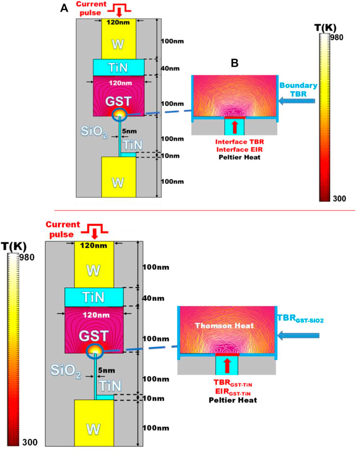
FIGURE 2. (A) Geometrical parameters of the designed blade-type PCRAM. (B) Zoom in of the area inside the blue circle shows the locations where different TBR, EIR and TE effects are defined. TBR is defined at GST-TiN heater and GST-SiO2 interfaces, while EIR is only given at GST-TiN heater interface. Thomson heat occurs at the bulk GST and bulk TiN heater, whereas Peltier heat takes place at GST-TiN heater interface. Color map inside the blue circle indicates the temperature contours inside the GST layer during the “RESET” operation, and the corresponding isothermal values are illustrated on the leftmost side. Such temperature contours are induced by a 20 μA current pulse of 60 ns.
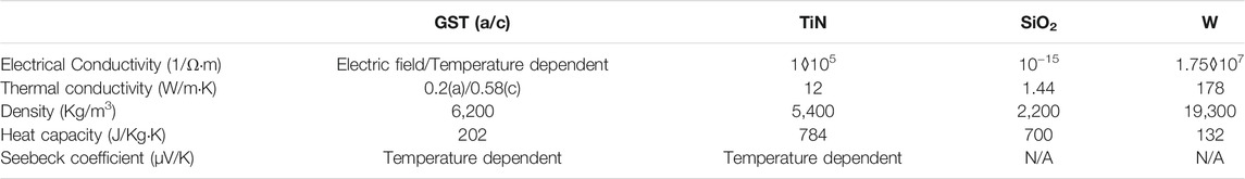
TABLE 1. Characteristic values used for simulations.
Results and Discussions
A series of current pulses with various amplitudes and a fixed period of 60 ns (5 ns rising, 50 ns plateau, and 5 ns trailing) are employed here to assess the dependence of TE effects, TBR, and EIR on resulting programming currents. After each write operation, a readout current whose amplitude is 0.01 times the peak value of the corresponding write current, is implemented to read the device resistance. The schematic of the adopted write and read currents are given in Figure 3A. We first investigate the influence of the TE effects on amorphization current without taking into account any TBR and EIR, as illustrated in Figure 3B. It is found that the device resistance undergoes an abrupt increase when write current increases to 50.5 and 51.5 μA for positive (i.e., current flows from top to bottom electrodes) and negative (current flow from bottom to top electrodes), respectively. Such resistance increase obviously arises from the advent of the amorphous region that fully covers the GST-TiN interfacial region. As the negative polarity of the TE effects in fact cools the active region of the PCRAM device, the temperature inside the GST layer is lower than that obtained from the positive current polarity. In this case, the positive current polarity leads to a lower programming current when compared to negative current polarity. However, it is evident that the cooling effect from the negative current polarity is not pronounced due to the slight programming current variation between positive and negative current polarity. Subsequently, the EIR is introduced into our developed model, and the integration of TE effects with the EIR factor results in Figure 3C. As can be seen from Figure 3C, the required programming current to trigger aforementioned resistance switching decreases to 48 and 49.5 μA for positive and negative current polarities, respectively. Although the presence of EIR makes the device more resistive, it also enhances the resistive heating (i.e., Joule heating) at the GST-TiN interface when compared to the case without EIR. This consequently reduces the programming current. In addition to EIR, the influences of TBRGST-TiN and TBRGST-SiO2 on the programming current for positive and negative current polarities are also studied and depicted in Figures 3D,E, respectively. In terms of TBRGST-TiN, the programming current changes to 50 and 52 μA for positive and negative polarities, respectively. For the case of positive current polarity, the TBR GST-TiN prevents part of Joule heating from dissipating into the TiN heater, which thus decreases the programming current to some extent. In contrast, less heating energy is transferred to the GST layer due to the inhibition of the TBRGST-TiN in terms of negative current polarity, thereby requiring higher programming current. More importantly, the programming current for both cases is reduced to ∼27 μA when considering the TBR GST-SiO2 exclusively. This undoubtedly implies that the TBR GST-SiO2 can drastically suppress the heat diffusion through the SiO2 insulation, and thus maintain Joule heating inside the active region to the utmost extent. As a result, the cooling phenomenon stemming from the negative current polarity has a negligible effect on resulting temperature inside the GST layer, which makes the programming current of the positive current polarity case coincide with that of the negative current polarity case. Based on the results above, we eventually include TBRGST-TiN, TBRGST-SiO2, and EIR into the developed model, and re-calculate the programming current for both positive and negative current polarities, leading to Figure 3F. Owing to the effects of EIR and TBR GST-TiN, the programming current is found to be 17 and 19.5 μA for positive and negative current polarities, respectively, giving rise to an increase of 11%.
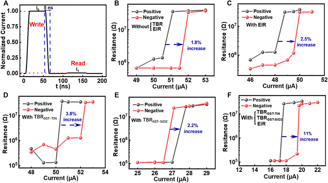
FIGURE 3. (A) The schematic of the adopted write and read current pulse, and the dependence of the device resistance on the programming current with positive and negative polarities for the case (B) without TBR and EIR, (C) only with EIR, (D) only with TBRGST-TiN, (E) only with TBRGST-SiO2, and (F) with both TBR and EIR. Note that the TE effects are included into all cases.
According to Figure 3, TBR plays a more important role on determining the programming current than EIR when considering the TE effects. Given this fact, the possible influence of TBR on resulting TE effects is further explored by virtue of the calculated power density, depicted in Figure 4. Figure 4A shows the power density arising from the Thomson heat only for both positive and negative current polarities, while ignoring the TBR effect. It is revealed that the calculated power density for the positive current polarity is classified into three levels inside the active region, denoted by light green, dark red, and light blue, respectively. However, the polarity of the Thomson heat inside the TiN heater remains negative, opposite to that of the active GST region. Similar to the positive polarity, the negative current polarity also gives rise to three power density levels, while having the negative power density inside the TiN heater. Such polarity deviation between GST and TiN heater regions obviously weakens the total heating effects inside the active region, inducing higher programming current. Such drawback can be excitingly alleviated according to the presence of the TBR GST-SiO2 and TBR GST-TiN, as demonstrated in Figure 4B. As reflected in Figure 4B, the power density distributions possessed from the Thomson heat still exhibit three levels for both positive and negative current polarities. Nevertheless, the appearance of the TBR GST-SiO2 and TBR GST-TiN, assigns the power density inside the GST region with the same sign as that inside the TiN heater, which undoubtedly strengthens the heating effect and reduces the programming current. To verify and explain above hypothesis, we further plot the adopted Seebeck coefficients of the GST and TiN materials in our simulations, and calculated the power density distributions along the GST-TiN heater interfacial line for the cases with and without TBR, resulting in Figures 4C,D. According to Figure 4D, the power density along the defined interfacial line initially increases, suddenly drops to a negative value, and eventually remains positive for the case without TBR. As power density relies on both temperature and the gradient of the Seebeck coefficients (Eq. 4), the initial enhancement of the power density can be readily ascribed to the increased temperature inside the GST layer. Moreover, the temperature inside the TiN heater in this case remains low due to the lack of TBR, which gives rise to the positive gradient of the Seebeck coefficients. The power density inside the TiN heater becomes therefore negative, resulting in a sudden drop. Once the position where the power density is detected is inside the active region, its value returns to the positive sign. When taking into account the TBR, a gradual increase on the calculated power density inside the GST layer is witnessed owing to the enhanced temperature along the interfacial line. It should be kept in mind that the presence of the TBR significantly booms the temperature at the GST-TiN interface, thus triggering a negative sign of the Seebeck gradient inside the TiN heater. As the GST layer also allows for a negative Seebeck gradient at the same temperature zone, this clearly renders the power density polarity inside the active region same as that inside the TiN heater, thereby intensifying the TE effects and lowering the programming current.
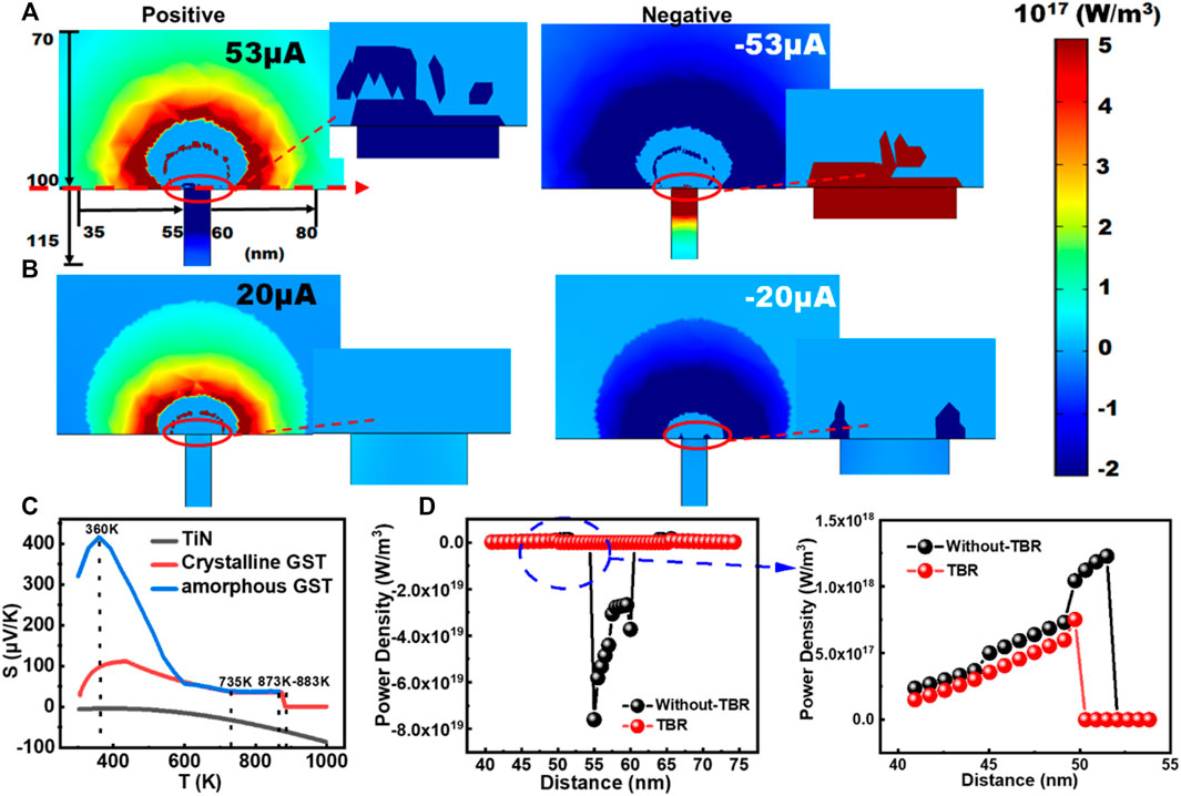
FIGURE 4. (A) Calculated power density distributions for the Thomson heat inside the designed device without the TBR effect for the cases with positive (left) and negative (right) polarities; (B) calculated power density distributions for the Thomson heat inside the designed device with the TBR effect for the cases with positive (left) and negative (right) polarities; (C) adopted Seebeck coefficients of the GST and TiN medium as a function of temperature. (D)calculated power densities along the GST-TiN heater interfacial line for the cases with and without TBR effects. The TE polarity here is assumed positive. Zoom-in on the areas bounded by red ovals in (A,B) exhibits the power density polarity comparisons between the GST and TiN heater, whereas zoom-in on the region bounded by blue oval in (D) shows the power densities values at this certain region. Note that the power densities are detected at the beginning of the pulse trailing edge (i.e., the end of the plateau edge). The pulse amplitudes for the cases with and without TBR are set to be 20 and 53 μA, respectively. (C) is reprinted with permission from (Faraclas et al., 2014).
The dependence of power density polarity on temperature is further testified in Figure 5 with respect to different time moments. The calculated power density and temperature contours at different time moments of the applied pulse (i.e., 8, 11, and 14 ns) are depicted in Figures 5A,B, respectively. It is found that at 8 ns, the sole region where temperature exceeds 400 K is near the GST-TiN heater interface. As a result, the region near the GST-TiN heater interface gives rise to an opposite polarity sign of the Seebeck coefficient gradient to the rest of the active region. This obviously makes the polarity of the calculated power density near the interfacial region contrary to the rest of the GST layer, as reflected in the leftmost portion of Figure 5A. Along with time elapsing (e.g., 11 ns), the temperature near the interface varies between 735 and 835 K, which results in a positive Seebeck gradient, and a negative power density polarity. In contrast, the temperature at the rest of the active region is smaller than 735 K, while higher than 400 K. This in turn leads to a negative Seebeck gradient and a positive power density polarity. When the previously formed amorphous region further expands and occupies majority of the active region (14 ns), the temperature inside majority of the active region exceeds 900 K, corresponding to a zero Seebeck gradient. The resulting power density is therefore detected to be approximately zero.
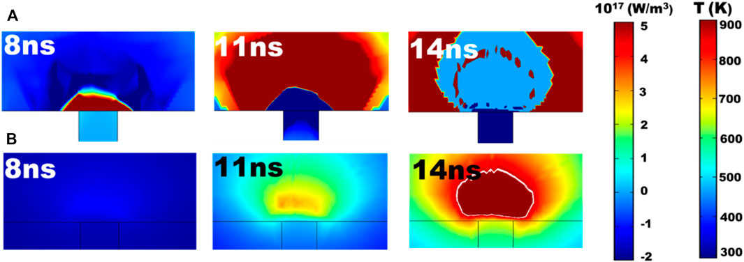
FIGURE 5. (A) Calculated power density distributions for the Thomson heat inside the designed device without the TBR effect at 8 ns (left), 11 ns (middle), and 14 ns (right) of the programming current pulse. (B) Calculated temperature distributions inside the designed device without the TBR effect at 8 ns (left), 11 ns (middle), and 14 ns (right) of the programming current pulse. The pulse amplitude is considered as 53 μA. The left and right color maps correspond to (A,B), respectively.
It is clearly indicated from aforementioned results that the TBR can effectively reduce the heat escape either from the TiN heat or SiO2 insulation, and remarkably enhance the temperature inside the active region, particularly at the GST-TiN interface. Such temperature increase has a significant impact on the power density polarity, and choosing appropriate TBRs enables the same power density polarity inside both the active GST region and TiN heater, which further mitigates the total heating effect and triggers lower programming current. As the TBRGST-SiO2 exhibits a closer pertinence to the TE effects than the TBRGST-TiN, different programming current required to induce a device resistance of ∼30 MΩ (i.e., the maximum device resistance achieved in Figure 3) for both positive and negative polarities are calculated with respect to TBRGST-insulation, and their decrement when compared to the cases without the TBRGST-insulation, are illustrated in Figure 6A. Note that here we artificially define the TBR range at GST-surrounding insulation interface to optimize its value. In this case we use TBRGST-insulation to replace TBRGST-SiO2, considering that the optimized insulation may not be made of SiO2. According to Figure 6A, the programming current decrement with the positive polarity varies from 12.5 to 31% with TBRGST-insulation ranging from 1◊10−5 cm2·K/W to 5◊10−5 cm2·K/W. On the one hand, increasing the TBRGST-insulation can to the utmost extent suppress the heat diffusion through the encapsulation, and enhance the Joule heating effect. On the other hand, using larger TBRGST-insulation can increase the temperature inside the active region, and can consequently strengthen the TE effects at the GST-TiN heater interface. The combination of above two factors contributes to the programming current reduction. The programming current decrement with the negative polarity follows the similar trend to the positive polarity. Another intriguing finding is that, since the TBR can partially circumvent the unwanted cooling from the negative current polarity, the calculated programming current decrement for the negative polarity is slightly larger than that for the positive polarity. Nevertheless, the required negative programming current to achieve a device resistance of ∼30 MΩ is smaller than the positive current by 10% regardless of the TBRinsulation. In addition to TBR, device scaling is another key factor that determines the programming current. To study such influence, the diameter of the interfacial region alters from 5 to 50 nm and the interrelated programming current for both positive and negative polarities are calculated, leading to Figure 6B. It is indicated in Figure 6B that expanding the contact diameter from 5 to 50 nm results in an increase on the positive polarity current from 50 to 400 μA. This is expected, as using a wider diameter enlarges the GST-heater interface and thus needs much higher current to amorphized such region. Further observation also shows that the negative polarity current varies analogously to the positive current along with the same diameter range. Due to the inherent cooling effect, the negative polarity current is always higher than the positive current for a given diameter. The polarity current difference between positive and negative polarities initially decreases with a contact diameter smaller than 25 nm, after which it begins to increase. It is pointed out that the polarity current difference is calculated by (Inegative–Ipositive)/Inegative where Inegative and Ipositive are the calculated negative and positive polarity current, respectively. The larger diameter undoubtedly increases the programming current that is employed as the denominator of the above expression, which therefore decreases the calculated current difference. However, further enlarging the interfacial size exacerbates the cooling effect through the interface and requires much higher negative polarity current for amorphization. This in turn increases the numerator value of above expression and increase the current difference. It should be also noticed that either enlarging or shrinking the interfacial size solely cannot affect the temperature distribution near the GST-TiN heater interface and is thus insensitive to the resulting power density polarity. This essentially requires appropriate TBR values for different device scaling so as to maximize both Joule heating and TE heating effects.
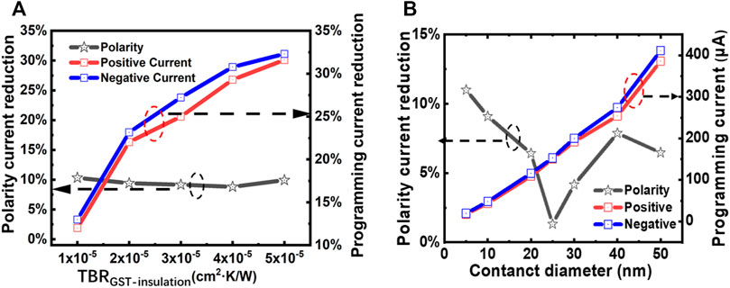
FIGURE 6. (A) Required programming current decrement to induce a device resistance of ∼30 MΩ for both positive (red) and negative (blue) current polarities when compared to the cases without TBR and the calculated polarity current difference (black) with respect to the TBR at GST-insulation interface. (B) Required programming current to induce a device resistance of ∼30 MΩ for both positive (red) and negative (blue) current polarities and the calculated polarity current difference (black) with respect to the contact diameter of the interfacial region. For both cases TE effects are included.
Conclusion
Impacts of the TBR and EIR on resulting TE effects are investigated here for the blade-type PCRAM architecture according to a well-developed electro-thermal and phase-change transformation model. Results clearly indicate that the TBR at GST-SiO2 insulation plays a dominant role in determining the interfacial temperature and required amorphization current for positive and negative polarities in comparison with the TBR at GST-heater interface and EIR at GST-heater interface. The presence of the TBR can largely enhance the interfacial temperature and change the Seebeck gradient of the active and heater regions. Adopting appropriate TBR can therefore lead to the same power density polarity for active and heater regions, thereby considerably improving the heating efficiency. Although solely changing the contact diameter of the interfacial region allows for the change of required polarity current, it is unable to switch the power density polarity and thus has a less pronounced influence on the TE effects than the TBR. It is therefore necessary to further optimize the TBR for different device scaling in order to facilitate the heating efficiency.
Data Availability Statement
The raw data supporting the conclusion of this article will be made available by the authors, without undue reservation.
Author Contributions
Conceptualization, XjL and LW; methodology, XjL, JF and WR; software, JF, ZG, XyL, and XW; validation, QR, JW and CY; writing-original draft preparation, XjL, XyL and LW; writing-review and editing, LW. All authors have read and agreed to the published version of the manuscript.
Funding
This work was supported by the National Science Foundation of China (Grant Nos. 61964012, 61804079, 61904089, 61904087), the Science and Technology Department of Jiangsu Province (Grant Nos. BK20190731, BK20211273 and BZ2021031), the Science Foundation of National and Local Joint Engineering Laboratory of RF Integration and Micro-Assembly Technology (Grant Nos. KFJJ20200102 and KFJJ20200203), the Industry Program of Huzhou City (Grant No.2020GG03), the Institution of Jiangsu Province (Grant No. 2020KJB510014), the NUPTSF (Grant Nos. NY220078 and NY220112), Foundation of Jiangxi Science and Technology Department (Grant No. 20202ACBL212001), Funding of innovative and entrepreneurial doctor (JSSCBS20210522), and the science and technology department of Jiangxi Province under Grant no 20202BABL202028.
Conflict of Interest
The authors declare that the research was conducted in the absence of any commercial or financial relationships that could be construed as a potential conflict of interest.
Publisher’s Note
All claims expressed in this article are solely those of the authors and do not necessarily represent those of their affiliated organizations, or those of the publisher, the editors and the reviewers. Any product that may be evaluated in this article, or claim that may be made by its manufacturer, is not guaranteed or endorsed by the publisher.
References
Adam, A. A. E. (2020). Proposal for a Universal Nonvolatile Logic Device Based on the Phase Change Magnetic Material. Appl. Phys. A. 126, 918–1010. doi:10.1007/s00339-020-04096-y
Aoki, I. (2003). A Study on a Phase-Change Disc and a Dye-Material Disc Using a Spin-Coating Method for Low-Cost and High-Speed Recording. Proc. SPIE 5069, 124–129. doi:10.1117/12.532427
Bedolla, E., Padierna, L. C., and Castañeda-Priego, R. (2021). Machine Learning for Condensed Matter Physics. J. Phys. Condens. Matter 33, 053001–053006. doi:10.1088/1361-648x/abb895
Chen, Y., Zhang, L., Liu, J., Lin, X., Xu, W., Yue, Y., et al. (2019). Ferroelectric Domain Dynamics and Stability in Graphene Oxide-P(VDF-TrFE) Multilayer Films for Ultra-High-Density Memory Application. Carbon 144, 15–23. doi:10.1016/j.carbon.2018.12.013
Choi, H.-S., Kim, H., Lee, J.-H., Park, B.-G., and Kim, Y. (2020). AND Flash Array Based on Charge Trap Flash for Implementation of Convolutional Neural Networks. IEEE Electron. Device Lett. 41, 1653–1656. doi:10.1109/led.2020.3025587
Dongale, T. D., Khot, A. C., Takaloo, A. V., Son, K. R., and Kim, T. G. (2021). Multilevel Resistive Switching and Synaptic Plasticity of Nanoparticulated Cobaltite Oxide Memristive Device. J. Mater. Sci. Techn. 78, 81–91. doi:10.1016/j.jmst.2020.10.046
Faraclas, A., Bakan, G., Adnane, L. H., Dirisaglik., F., Williams, N. E., Gokirmak, A., et al. (2014). Modeling of Thermoelectric Effects in Phase Change Memory Cells. IEEE Trans. Electron. Devices 61, 372–378. doi:10.1109/ted.2013.2296305
Feldmann, J., Stegmaier, M., Gruhler, N., Ríos, C., Bhaskaran, H., Wright, C. D., et al. (2017). Calculating with Light Using a Chip-Scale All-Optical Abacus. Nat. Commun. 8, 1256–1263. doi:10.1038/s41467-017-01506-3
Gunzel, M., Hakert, C., Chen, K. H., and Chen, J. J. (2021). Heart: Hybrid Memory and Energy-Aware Real-Time Scheduling for Multi-Processor Systems. ACM Trans. Embedded Comput. Syst. 20, 88–93. doi:10.1145/3477019
Han, X.-F., Laga, H., and Bennamoun, M. (2021). Image-Based 3D Object Reconstruction: State-Of-The-Art and Trends in the Deep Learning Era. IEEE Trans. Pattern Anal. Mach. Intell. 43, 1578–1604. doi:10.1109/tpami.2019.2954885
Howard, G., Bull, L., de Lacy Costello, B., Gale, E., and Adamatzky, A. (2014). Evolving Spiking Networks with Variable Resistive Memories. Evol. Comput. 22, 79–103. doi:10.1162/evco_a_00103
Indiveri, G., and Liu, S.-C. (2015). Memory and Information Processing in Neuromorphic Systems. Proc. IEEE 103, 1379–1397. doi:10.1109/jproc.2015.2444094
Jin, Q.-X., Liu, B., Liu, Y., Wang, W.-W., Wang, H., Xu, Z., et al. (2016). Three-Dimensional Simulations of RESET Operation in Phase-Change Random Access Memory with Blade-type like Phase Change Layer by Finite Element Modeling. Chin. Phys. Lett. 33, 098502–098510. doi:10.1088/0256-307x/33/9/098502
Jing, L., and Tian, Y. (2021). Self-Supervised Visual Feature Learning with Deep Neural Networks: A Survey. IEEE Trans. Pattern Anal. Mach. Intell. 43, 4037–4058. doi:10.1109/tpami.2020.2992393
Kwon, Y., Park, B., and Kang, D.-H. (2015). Scaling of Data Retention Statistics in Phase-Change Random Access Memory. IEEE Electron. Device Lett. 36, 454–456. doi:10.1109/led.2015.2414952
LeCun, Y., Bengio, Y., and Hinton, G. (2015). Deep Learning. Nature 521, 436–444. doi:10.1038/nature14539
Lee, J., Asheghi, M., and Goodson, K. E. (2012). Impact of Thermoelectric Phenomena on Phase-Change Memory Performance Metrics and Scaling. Nanotechnology 23, 205201–205210. doi:10.1088/0957-4484/23/20/205201
Liu, J., and Chen, S. (2020). Initial Experience with 3D XPoint Main Memory. Distrib. Parallel Databases 38, 865–880. doi:10.1007/s10619-019-07277-8
Navarro, G., Sousa, V., Persico, A., Pashkov, N., Toffoli, A., Bastien, J.-C., et al. (2013). Material Engineering of GexTe100−x Compounds to Improve Phase-Change Memory Performances. Solid State Electron. 89, 93–100. doi:10.1016/j.sse.2013.07.005
Ni, K., Yin, X. Z., Laguna, A. F., Joshi, S., Dunkel, S., Trentzsch, M., et al. (2019). Ferroelectric Ternary Content-Addressable Memory for One-Shot Learning. Nat. Electron. 2, 521–529. doi:10.1038/s41928-019-0321-3
Noori, Y. J., Meng, L., Jaafar, A. H., Zhang, W., Kissling, G. P., Han, Y., et al. (2021). Phase-Change Memory by GeSbTe Electrodeposition in Crossbar Arrays. ACS Appl. Electron. Mater. 3, 3610–3618. doi:10.1021/acsaelm.1c00491
Oh, S., Huang, Z., Shi, Y., and Kuzum, D. (2019). The Impact of Resistance Drift of Phase Change Memory (PCM) Synaptic Devices on Artificial Neural Network Performance. IEEE Electron. Device Lett. 40, 1325–1328. doi:10.1109/led.2019.2925832
Patel, U. K., Anwar, A., Saleem, S., Malik, P., Rasul, B., Patel, K., et al. (2021). Artificial Intelligence as an Emerging Technology in the Current Care of Neurological Disorders. J. Neurol. 268, 1623–1642. doi:10.1007/s00415-019-09518-3
Pieterson, L. v., Rijpers, J. C. N., and Hellmig, J. (2004). Phase-Change Media for Ultrahigh-Speed Digital Versatile Disc Recording. Jpn. J. Appl. Phys. 43, 4974–4977. doi:10.1143/jjap.43.4974
Sebastian, A., Le Gallo, M., and Eleftheriou, E. (2019). Computational Phase-Change Memory: Beyond von Neumann Computing. J. Phys. D Appl. Phys. 52, 443002–443010. doi:10.1088/1361-6463/ab37b6
Umesh, S., and Mittal, S. (2019). A Survey of Spintronic Architectures for Processing-In-Memory and Neural Networks. J. Syst. Archit. 97, 349–372. doi:10.1016/j.sysarc.2018.11.005
Wang, L., Lu, S. R., and Wen, J. (2017). Recent Advances on Neuromorphic Systems Using Phase-Change Materials. Nanoscale Res. Lett. 12, 347–422. doi:10.1186/s11671-017-2114-9
Wang, H., Liu, Y., Liu, B., Gao, D., Xu, Z., Zhan, Y., et al. (2017). Nanoscale Cross-Point Diode Array Accessing Embedded High Density PCM. Semicond. Sci. Technol. 32, 085009–85108. doi:10.1088/1361-6641/aa7520
Wang, H., Li, S., Song, L., and Cui, L. (2019). A Novel Convolutional Neural Network Based Fault Recognition Method via Image Fusion of Multi-Vibration-Signals. Comput. Industry 105, 182–190. doi:10.1016/j.compind.2018.12.013
Wen, J., and Wang, L. (2020). Interfacial Resistance Characterization for Blade-type Phase Change Random Access Memory. IEEE Trans. Electron. Devices 67, 968–975. doi:10.1109/ted.2020.2965187
Wright, C. D., Armand, M., and Aziz, M. M. (2006). Terabit-Per-Square-Inch Data Storage Using Phase-Change Media and Scanning Electrical Nanoprobes. IEEE Trans. Nanotechn. 5, 50–61. doi:10.1109/tnano.2005.861400
Zhang, W., Gao, B., Tang, J., Yao, P., Yu, S., Chang, M.-F., et al. (2020). Neuro-inspired Computing Chips. Nat. Electron. 3, 371–382. doi:10.1038/s41928-020-0435-7
Keywords: thermoelectric, thermal boundary resistance, reset, GST, scaling, modelling
Citation: Lian X, Fu J, Gao Z, Ren W, Wan X, Ren Q, Wen J, Yang C, Liu X and Wang L (2022) Impact of Thermal Boundary Resistance on Thermoelectric Effects of the Blade-Type Phase-Change Random Access Memory Device. Front. Mater. 8:798398. doi: 10.3389/fmats.2021.798398
Received: 21 October 2021; Accepted: 01 December 2021;
Published: 03 January 2022.
Edited by:
Zhengfei Dai, Xi’an Jiaotong University, ChinaReviewed by:
Han Jin, Shanghai Jiao Tong University, ChinaJin Wu, Sun Yat-sen University, China
Hongbo Geng, Changshu Institute of Technology, China
Copyright © 2022 Lian, Fu, Gao, Ren, Wan, Ren, Wen, Yang, Liu and Wang. This is an open-access article distributed under the terms of the Creative Commons Attribution License (CC BY). The use, distribution or reproduction in other forums is permitted, provided the original author(s) and the copyright owner(s) are credited and that the original publication in this journal is cited, in accordance with accepted academic practice. No use, distribution or reproduction is permitted which does not comply with these terms.
*Correspondence: Xiaoyan Liu, eGlhb3lhbmxpdUBuanVwdC5lZHUuY24=; Lei Wang, bGVpd2FuZzE5ODBAbmp1cHQuZWR1LmNu