 Zhao Wang1†
 Xuan Wei
 Qichang Hu
- 1College of Mechanical and Electrical Engineering, Fujian Agriculture and Forestry University, Fuzhou, China
- 2State Key Laboratory of Optoelectronic Materials and Technologies, School of Materials, Sun Yat-sen University, Guangzhou, China
- 3National Engineering Research Center for Optoelectronic Crystalline Materials, Fujian Institute of Research on the Structure of Matter, Chinese Academy of Sciences, Fuzhou, China
- 4Key Laboratory of Optoelectronic Materials Chemistry and Physics, Chinese Academy of Sciences, Fuzhou, China
Graphene (Gr) has high transmittance to ultraviolet (UV) light and high mobility, which can effectively collect and transfer carriers. In this work, MgZnO (MZO) films were grown on the surface of the p-GaN by magnetron sputtering. A heterojunction solar-blind UV detector with Gr/MZO/GaN structure was constructed by introducing Gr as the window layer film. The test results show that the device has excellent detection ability for solar-blind UV light. The light response cut-off edge of the device is 263 nm, under the illumination of 255 nm and the bias voltage of −5 V, the responsivity is 14.6 mA/W, the rise time is 0.79 s, the decay time is 0.2 s, and the external quantum efficiency is 71.1%. The importance of this work lies in providing a reference for the application of Gr-based photodetectors.
Introduction
Semiconductor solar-blind UV detectors have attracted widespread attention from researchers and can be applied in many fields such as spatial data transmission, discharge detection in substations, etc (Xie et al., 2013; Xu et al., 2019; Klas et al., 2021). Among them, MZO, as one of the most common solar-blind UV wide band gap semiconductor materials (Zheng et al., 2015), has a continuously adjustable band gap width of 3.3–7.8 eV, and has the advantages of low defect density, high radiation resistance (Hou et al., 2011; Jyun-Yi et al., 2015; Tian et al., 2016; Hu and Kai, 2017).
Many works have shown that the quality of the photo-responsive layer film will also affect the performance of the detector. Too low quality of the film may result in slow response speed, poor frequency response and low responsivity of the detector (Zhang D. et al., 2018; Li et al., 2019). In addition, the vertical structure of the heterojunction detector has better performance than the planar structure of the MSM detector (Liang et al., 2016; Goswami et al., 2020; Wang et al., 2021). This is because the vertical structure of the device has a shorter transmission distance, and the heterojunction detector has a built-in electric field that promotes the transmission of carriers (Wu et al., 2010; Xie et al., 2018).
Therefore, in order to improve the device performance of the MZO heterojunction detector, it is necessary to start with the quality of the film and the structure of the device. At first, the quality of MZO film is related to its growth method, at present, a great deal of work has focused on improving the quality of MZO film (Li et al., 2011; Xie et al., 2012; Shiau et al., 2016; Rana et al., 2018). Yanmin Zhao et al. (Zhao et al., 2009) used magnetron sputtering to obtain high-quality MZO film. In this work, MZO films are also grown by RF magnetron sputtering (Kelly and Arnell, 2000). At the same time, the choice of the substrate also has a great influence on the quality of film. GaN has a lattice structure similar to MZO (Zhang et al., 2014) and has stable p-type material, it is an excellent substrate for growing MZO film. Secondly, as mentioned earlier, the construction of the heterojunction is the structural basis of junction detector, and the sandwich-like vertical structure is often adopted. In this vertical structure, the light absorption layer is located between two conductive layers. In this paper, Gr with an two-dimensional structure is introduced as the upper conductive layer. As a natural p-type material, it not only hardly absorbs solar-blind UV light, but also has a very high mobility (Allen et al., 2010; Zheng et al., 2018a; Zhang et al., 2019b; Hu et al., 2019), which can effectively collect the carriers generated in the light absorption layer.
To sum up, in this work, an MZO film was grown on the p-GaN substrate, and Gr was introduced to construct a heterojunction solar-blind UV detector with a vertical structure of p-Gr/MZO/p-GaN. Due to the absorption characteristics of the photoresponse layer (MZO film), the device has a selective response to solar-blind UV light, and its cut-off edge is 263 nm. Under solar-blind UV light, the rise time of the device under −5 V bias is 0.79 s, the decay time is 0.20 s, and its responsivity is 14.6 mA/W. This MZO-based photodetector also provides a reference for the application of Gr-based heterojunction detectors.
Materials and Methods
MZO Film Preparation
Magnetron sputtering was used to grow the MZO film. First, the GaN substrate was cleaned in an ultrasonic cleaning device with acetone, alcohol, and deionized water. After removing the water vapor on the surface of the GaN substrate, the GaN substrate was put into the sputtering chamber for sputtering. Introduce Ar and O2 into the sputtering chamber at the same time, their flow rates are both 20 sccm, and the atmosphere is maintained at 2 Pa during the sputtering process. The temperature of the substrate was controlled at 600°C, and the rotation speed was 20 rpm. Mg target and Zn target were sputtered at 60 W and 240 W power respectively. After 90 min of sputtering, the preparation of MZO/GaN has been completed.
Graphene Transfer
The single-layer Gr attained through commercial channel was used for this experiment, and it is a high-grade copper-based Gr grown by chemical vapor deposition. There are also detailed descriptions of Gr transfer in other works (Lin et al., 2018; Hu et al., 2019). First, spin-coated 5% (wt%) PMMA chlorobenzene solution on the surface of copper-based Gr and dried it, then used ammonium persulfate solution to corrode the copper foil, afterwards, PMMA/Gr was transferred to the MZO/GaN surface and washed three times in acetone, alcohol, and deionized water in order to ensure that all residues were completely removed. In this way, the transfer of Gr has been accomplished and the Gr evenly covered the surface of the MZO film. Figure 1 shows the facturing process of the Gr/MZO/GaN heterojunction.
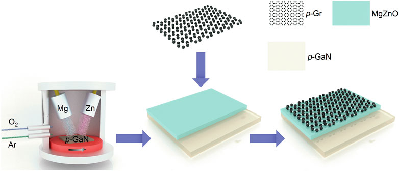
FIGURE 1. Fabrication process of Gr/MZO/GaN structure. The MZO film is grown first, and then the graphene transfer is performed.
Photodetector Fabrication
On the surface of Gr, a Ti/Au electrode was obtained by thermal evaporation, and an In electrode was obtained by welding on the GaN substrate. The Ti/Au electrode and In electrode form good ohmic contact or quasi-ohmic contact with Gr and GaN, respectively, which will not affect our photodetector test. At this point, the fabrication of the Gr/MZO/GaN heterojunction photodetector has been completed.
Characterizations and Measurements
We measured the characteristics of the MZO film. An X-ray Diffractometer (Rigaku MiniFlex 600) was used to study the crystallinity of the MZO film. The absorption spectrum of the MZO film was obtained by UV-VIS spectrophotometer (Shimadzu UV-2600). The surface morphology, thickness and element distribution of MZO film were measured by Focused Ion Beam etching system (ZEISSAURIGA) and atomic force microscope (CSPM 5500).
In addition, a Keithley 2636B source meter was used to measure the electrical characteristics of the device under various conditions. The light sources used in the measurement are all monochromatic light sources with wavelengths of 255 nm, 280 nm, 311 nm, 371 and 442 nm.
Results
Film Characterization Results
Figure 2A demonstrates the XRD result of MZO grown on GaN substrate. Due to the film thickness, there are very strong substrate diffraction peaks in the image, which leads to the weak signal peak of MZO film. However, three diffraction peaks (002), (111), (200) of the MZO film can still be observed, indicating that the MZO film is dominated by hexagonal phase and has good crystallinity (Senthil Kumar and Kumar, 2003; Wang et al., 2010; Young and Liu, 2018). The absorption spectrum of MZO film on sapphire substrate shown in Figure 2B, the preparation method and the conditions of MZO/sapphire structure and MZO/GaN structure are the same. The figure shows the absorption cut-off edge is 263 nm, on the basis of the connection between the band gap and the absorption value (Wu et al., 2010), we have made the corresponding band gap diagram by plotting the curve of (αhv)2 vs hv, where α means absorption coefficient, h means Planck constant, v means optical frequency. As shown in Figure 2B and the insertion diagram, we can see that the film has a sharp cut-off edge at 263 nm, the band gap width is 4.71 eV. The material with this band gap width can be used as the light photoresponse layer of solar-blind UV photodetectors. Figure 2C shows the surface morphology of MZO measured by Focused Ion Beam etching system and AFM, which shows that the surface of MZO film is smooth. Figure 2C also shows the element distribution of MZO film, the element of Mg and Zn is evenly distributed and the proportion of Mg component is 72.5% of the total of Mg and Zn. In addition, it can be seen from the cross-sectional SEM image in the figure that the thickness of the MZO film is 220 nm.
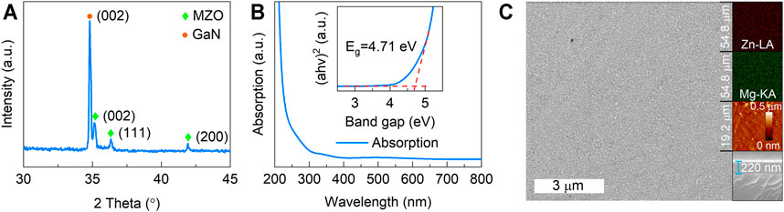
FIGURE 2. Characterization of MZO film. (A) XRD result of MZO film, which shows that the film is mainly hexagonal phase. (B) The absorption spectrum and band gap diagram of the MZO film, with a cut-off edge of 263 nm and a band gap of 4.71 eV. (C) The surface morphology, element distribution and thickness of MZO film. the element of Mg and Zn is evenly distributed, the surface of MZO film is smooth and its thickness is 220 nm.
Device Performance Measurements Results
The device is a heterojunction solar-blind photodetector with Gr/MZO/GaN structure. Figure 3A demonstrates the structure of the detector. MZO film is on the GaN substrate, and single-layer Gr is above MZO film. Ti/Au electrode and In electrode was fabricated on GaN and Gr side respectively. In this work, many tests have been carried out on the electrical characteristics of the device. Figure 3B shows the dark current curve under dark conditions and the photocurrent curve under 255 nm illumination. By comparison, it can be seen that the device has an obvious response to 255 nm light. When the device is in positive bias voltage, the photocurrent under 255 nm light is very close to the dark current, while in the negative bias voltage, the photocurrent of the device is nearly an order of magnitude greater than the dark current, which indicates that the device will have a very large signal-to-noise ratio under negative bias voltage, which is suitable for working under negative bias voltage. The dark current of the device has three different stages, which are analyzed by drawing the schematic diagram of the rectification principle as shown in Figure 3B-inset.The reverse-breakdown voltage of Gr/MZO junction is relatively high, while that of MZO/GaN junction is low. When the whole device is reverse biased, the Gr/MZO junction is in the reverse bias voltage, and the MZO/GaN junction is in the forward direction bias voltage, the whole device shows the current cut-off state. When the whole device is in forward bias, the Gr/MZO junction is in forward bias, but for the MZO/GaN junction in reverse bias, there are two cases: when the bias is small, the device is still in the current cut-off state; when the bias is large, the MZO/GaN junction is in the breakdown state, and the device is in the current on state (Zheng et al., 2018a). Moreover, this structure can effectively inhibit the thermal diffusion of positive and negative carriers in theory, which makes the noise current density of the device very low (Chi On et al., 2003), which is an additional significant advantage of the device.
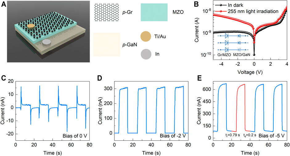
FIGURE 3. (A) Structure diagram of the device. (B) The I-V curve of the device under a dark environment and 255 nm illumination, the lower left corner reveals the schematic diagram of the device’s rectification principle. (C) When the device is under 0 bias voltage, the current changes with time, that is, the I-t curve, the rise time is 0.56 s, and the decay time is 0.21 s, the photocurrent is 2 nA. (D) The I-t curve under −2 V bias voltage has a rise time of 0.16 s and a decay time of 0.70 s, the photocurrent is 300 nA. (E) The I-t curve under −5 V bias voltage has a rise time of 0.79 s and a decay time of 0.20 s, the photocurrent is 670 nA.
In addition, the current curve of the device under 255 nm light with periodic switching was also tested. As the device is under 0 bias voltage, the device has obvious capacitance effect, as shown in Figure 3C, its rise time and decay time are 0.56 and 0.21 s respectively. Figure 3D and Figure 3E are the time-dependent curves of the current measured under −2 V and −5 V bias respectively, the photocurrent is 300 nA under −2 V bias and 670 nA under −5 V, which are two orders of magnitude greater than the photocurrent 2 nA at zero bias, and there exists no obvious capacitance effect. The time required for the device current to change from 10% of the maximum value to 90% of the maximum value is regarded as the rise time of the device (Kan et al., 2020), the rise time under −2 V bias is 0.16 s, and the rise time under −5 V bias is 0.79 s; by the same token, the time required for the current to change from 90% of the maximum value to 10% of the maximum value is also determined as the device decay time (Li et al., 2020), the decay time under −2 V bias is 0.70 s, and the decay time under −5 V bias is 0.20 s. In addition, the results of these three pictures also prove that the device has stable performance and can be used repeatedly.
In order to test the response of the device under different illumination densities, the devices were irradiated with 255 nm light sources with different illumination densities, and the corresponding current and voltage values were measured, and the I-V characteristic curve as shown in Figure 4A was made. It is apparent that under the same bias voltage, as the light density increases, the photoresponse current of the device also increases. In order to see the connection between the photoresponse current and the light density more intuitively, we have drawn the relationship between the current and the light density under different negative bias voltages. As Figure 4B proves, it follows that under five different negative bias voltages, the photo generated current increases with the growth of light density, forming a linear relationship. The responsivity R is an significant reference to study the optical response ability of the device, the responsivity R is defined as
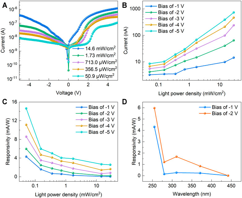
FIGURE 4. (A) The I-V characteristic curve of the device under 255 nm wavelength illumination with dissimilar current densities, the results indicated that under the same bias voltage, as the illumination density increases, the photoresponse current of the device also increases. (B) The graph of the current change with the light density under different bias voltages. The current increases as the light power density increases, forming a linear relationship. (C) The change of responsivity with light density. Due to the gradual saturation of carrier generation rate, the responsivity of the device decreases as light density increases. (D) Compared with the responsivity to the light of different wavelengths under −1 V and −2 V bias voltage, whence it followed that the responsivity at 255 nm is very high.
In addition, in order to determine whether the photogenerated carriers are mainly produced in MZO film, the spectral response characteristics of the devices was tested. Under multiple negative bias voltages, the photoresponse current of the device is measured with different wavelengths of light. After calculation, the selective optical response map of the device is drawn, as Figure 4D shows, it looks beyond dispute that under 255 nm illumination, the device has relatively obvious responsivity, while under 371 and 442 nm illumination, the responsivity is lower by more than an order of magnitude that under 255 nm illumination, which is in accordance with the optical absorption diagram measured as Figure 2A, indicating that the photogenerated carriers are the same as the original idea and mainly generated in the MZO layer. It is worth mentioning that the responsivity at 280 nm in this figure is lower than that at 311 nm, which is related to the fact that we did not use light with the same light power density.
The detector was compared with other detectors, and the relevant data is shown in Table 1. By comparison with the reference (Zhao et al., 2014), it can be seen that the responsivity of the detector in this paper is far greater than that of the MSM structure detector mentioned in the reference under the same bias voltage, the MSM detectors in some other articles (Wang et al., 2009; Zhao et al., 2015; Zhang W. et al., 2018), even if they work under a relatively high bias voltage, their responsivity is only comparable to the detectors in this article. It should be noted that the responsivity in the above-mentioned articles is the maximum value of its responsivity. In our test of responsivity, the shortest wavelength of the light source used is only 255 nm, which is far away from the wavelength at the absorption peak of MZO film. In other words, the responsivity of the detector in this paper will be far higher than 14.6 A/W in practical application, which indicates the detector in this article has excellent response performance. For this, we analyze that there are at least the following three reasons: First, the device uses Gr with high mobility and high light transmittance as the window layer to establish a vertical structure, which is beneficial to the transfer of photogenerated carriers; second, high quality MZO film is fabricated as optical absorption layer, which means that the recombination of photo-generated carriers due to trapping will be significantly reduced and, naturally, the photo-generated current generated by the device will increase; The p-Gr/MZO/p-GaN structure of the device can not only suppress noise electricity, but also contribute to the separation and transfer of photo-generated electron-hole pairs.
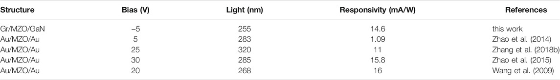
TABLE 1. Detector performance comparison.
Discussion
All in all, this work first uses magnetron sputtering to grow a high-quality MZO film on a p-type GaN substrate. Then the p-type single-layer Gr is introduced to form a heterojunction solar-blind UV detector with a Gr/MZO/GaN vertical structure, which has good response characteristics. The light response cut-off edge of the device is 263 nm, when expose to 255 nm light, the rise time of the device under −5 V bias is 0.79 s, the decay time is 0.2 s, its responsivity is 14.6 mA/W. In this article, we verified the feasibility and advantages of Gr as a window layer, and analyzed the reasons for the good performance of the device from multiple aspects in this article. More importantly, the MZO-based photodetector provides a reference for the application of Gr heterojunction detectors, and the construction method can also be used in the construction of other detectors, thereby improving the performance of other photodetectors.
Data Availability Statement
The raw data supporting the conclusions of this article will be made available by the authors, without undue reservation.
Author Contributions
ZW: Experiment, Data curation, Discussion, Writing. JL: Experiment, Data curation, Discussion. XW: Discussion. WZ: Conceptualization, Discussion. QH|: Conceptualization, Discussion, Writing.
Conflict of Interest
The authors declare that the research was conducted in the absence of any commercial or financial relationships that could be construed as a potential conflict of interest.
Publisher’s Note
All claims expressed in this article are solely those of the authors and do not necessarily represent those of their affiliated organizations, or those of the publisher, the editors and the reviewers. Any product that may be evaluated in this article, or claim that may be made by its manufacturer, is not guaranteed or endorsed by the publisher.
Acknowledgments
The authors gratefully acknowledge the support of Fund of National Engineering Research Center for Optoelectronic Crystalline Materials (OCM-2020-07), Science and Technology Innovation Special Fund Project of Fujian Agricultural and Forestry University (CXZX2020101A), Key Laboratory of Optoelectronic Materials Chemistry and Physics, Chinese Academy of Sciences (2008DP173016), Interdisciplinary integration promotes the development of smart agriculture (000/71202103B).
References
Allen, M. J., Tung, V. C., and Kaner, R. B. (2010). Honeycomb Carbon: a Review of Graphene. Chem. Rev. 110 (1), 132–145. doi:10.1021/cr900070d
Boruah, B. D., Mukherjee, A., and Misra, A. (2016). Sandwiched Assembly of ZnO Nanowires between Graphene Layers for a Self-Powered and Fast Responsive Ultraviolet Photodetector. Nanotechnology 27 (9), 095205. doi:10.1088/0957-4484/27/9/095205
Chi On Chui, C., Okyay, A. K., and Saraswat, K. C. (2003). Effective Dark Current Suppression with Asymmetric MSM Photodetectors in Group IV Semiconductors. IEEE Photon. Technol. Lett. 15 (11), 1585–1587. doi:10.1109/lpt.2003.818683
Goswami, L., Aggarwal, N., Verma, R., Bishnoi, S., Husale, S., Pandey, R., et al. (2020). Graphene Quantum Dot-Sensitized ZnO-Nanorod/GaN-Nanotower Heterostructure-Based High-Performance UV Photodetectors. ACS Appl. Mater. Inter. 12 (41), 47038–47047. doi:10.1021/acsami.0c14246
Hou, Y. N., Mei, Z. X., Liu, Z. L., Zhang, T. C., and Du, X. L. (2011). Mg0.55Zn0.45O Solar-Blind Ultraviolet Detector with High Photoresponse Performance and Large Internal Gain. Appl. Phys. Lett. 98 (10), 103506. doi:10.1063/1.3563705
Hu, Q.-C., and Kai, D. (2017). Magnesium Incorporation Efficiencies in Mg X Zn 1− X O Films on ZnO Substrates Grown by Metalorganic Chemical Vapor Deposition. Chin. Phys. B 26 (6), 068104. doi:10.1088/1674-1056/26/6/068104
Hu, Q., Zheng, W., Lin, R., Xu, Y., and Huang, F. (2019). Oxides/graphene Heterostructure for Deep-Ultraviolet Photovoltaic Photodetector. Carbon 147, 427–433. doi:10.1016/j.carbon.2019.03.027
Jia, L., Zheng, W., and Huang, F. (2020). Vacuum-ultraviolet Photodetectors. PhotoniX 1 (1), 22. doi:10.1186/s43074-020-00022-w
Jyun-Yi Li, L., Sheng-Po Chang, C., Hung-Hsu Lin, L., and Shoou-Jinn Chang, C. (2015). High Responsivity MgxZn1−xO Film UV Photodetector Grown by RF Sputtering. IEEE Photon. Technol. Lett. 27 (9), 978–981. doi:10.1109/lpt.2015.2405011
Kan, H., Zheng, W., Fu, C., Lin, R., Luo, J., and Huang, F. (2020). Ultrawide Band Gap Oxide Nanodots (Eg > 4.8 eV) for a High-Performance Deep Ultraviolet Photovoltaic Detector. ACS Appl. Mater. Inter. 12 (5), 6030–6036. doi:10.1021/acsami.9b17679
Kelly, P. J., and Arnell, R. D. (2000). Magnetron Sputtering: a Review of Recent Developments and Applications. Vacuum 56 (3), 159–172. doi:10.1016/s0042-207x(99)00189-x
Klas, R., Kirsche, A., Gebhardt, M., Buldt, J., Stark, H., Hädrich, S., et al. (2021). Ultra-short-pulse High-Average-Power Megahertz-Repetition-Rate Coherent Extreme-Ultraviolet Light Source. PhotoniX 2 (1), 4. doi:10.1186/s43074-021-00028-y
Li, G., Zhang, J., Liu, Y., and Zhang, K. (2011). Solar-blind Photodetectors Based on Polycrystalline MgZnO Thin Films. Opt. Eng. 50 (11), 113801. doi:10.1117/1.3643722
Li, Y., Zhang, D., Lin, R., Zhang, Z., Zheng, W., and Huang, F. (2019). Graphene Interdigital Electrodes for Improving Sensitivity in a Ga2O3:Zn Deep-Ultraviolet Photoconductive Detector. ACS Appl. Mater. Inter. 11 (1), 1013–1020. doi:10.1021/acsami.8b14380
Li, Y., Zheng, W., and Huang, F. (2020). All-silicon Photovoltaic Detectors with Deep Ultraviolet Selectivity. PhotoniX 1 (1), 15. doi:10.1186/s43074-020-00014-w
Liang, F.-X., Zhang, D.-Y., Wang, J.-Z., Kong, W.-Y., Zhang, Z.-X., Wang, Y., et al. (2016). Highly Sensitive UVA and Violet Photodetector Based on Single-Layer Graphene-TiO_2 Heterojunction. Opt. Express 24 (23), 25922–25932. doi:10.1364/OE.24.025922
Lin, R., Zheng, W., Zhang, D., Zhang, Z., Liao, Q., Yang, L., et al. (2018). High-Performance Graphene/β-Ga2O3 Heterojunction Deep-Ultraviolet Photodetector with Hot-Electron Excited Carrier Multiplication. ACS Appl. Mater. Inter. 10 (26), 22419–22426. doi:10.1021/acsami.8b05336
Rana, V. S., Rajput, J. K., Pathak, T. K., and Purohit, L. P. (2018). Multilayer MgZnO/ZnO Thin Films for UV Photodetectors. J. Alloys Comp. 764, 724–729. doi:10.1016/j.jallcom.2018.06.139
Senthil Kumar, M., and Kumar, J. (2003). XRD, XPS, SEM, PL and Raman Scattering Analysis of Synthesised GaN Powder. Mater. Chem. Phys. 77 (2), 341–345. doi:10.1016/s0254-0584(02)00012-3
Shiau, J.-S., Brahma, S., Liu, C.-P., and Huang, J.-L. (2016). Ultraviolet Photodetectors Based on MgZnO Thin Film Grown by RF Magnetron Sputtering. Thin Solid Films 620, 170–174. doi:10.1016/j.tsf.2016.09.037
Tian, C., Jiang, D., Pei, J., Sun, L., Liu, R., Guo, Z., et al. (2016). Performance Enhancement of MgZnO-Based Visible-Blind Photodetectors by Pt Nanoparticles. J. Alloys Comp. 667, 65–68. doi:10.1016/j.jallcom.2016.01.182
Wang, L. K., Ju, Z. G., Shan, C. X., Zheng, J., Li, B. H., Zhang, Z. Z., et al. (2010). Epitaxial Growth of High Quality Cubic MgZnO Films on MgO Substrate. J. Cryst. Growth 312 (7), 875–877. doi:10.1016/j.jcrysgro.2010.01.009
Wang, L. K., Ju, Z. G., Shan, C. X., Zheng, J., Shen, D. Z., Yao, B., et al. (2009). MgZnO Metal-Semiconductor-Metal Structured Solar-Blind Photodetector with Fast Response. Solid State. Commun. 149 (45-46), 2021–2023. doi:10.1016/j.ssc.2009.08.030
Wang, Z., Zheng, W., Hu, Q., Lin, S., Wu, Y., and Ye, D. (2021). Pt/(InGa)2O3/n-Si Heterojunction-Based Solar-Blind Ultraviolet Photovoltaic Detectors with an Ideal Absorption Cutoff Edge of 280 Nm. ACS Appl. Mater. Inter. 13 (37), 44568–44576. doi:10.1021/acsami.1c13006
Wu, C., Lu, Y., Shen, D., and Fan, X. (2010). Effect of Mg Content on the Structural and Optical Properties of Mg X Zn1−x O Alloys. Chin. Sci. Bull. 55 (1), 90–93. doi:10.1007/s11434-009-0393-y
Xie, C., Wang, Y., Zhang, Z.-X., Wang, D., and Luo, L.-B. (2018). Graphene/Semiconductor Hybrid Heterostructures for Optoelectronic Device Applications. Nano Today 19, 41–83. doi:10.1016/j.nantod.2018.02.009
Xie, X. H., Zhang, Z. Z., Li, B. H., Wang, S. P., Jiang, M. M., Shan, C. X., et al. (2013). Mott-type MgxZn1-xO-Based Visible-Blind Ultraviolet Photodetectors with Active Anti-reflection Layer. Appl. Phys. Lett. 102 (23), 231122. doi:10.1063/1.4811153
Xie, X. H., Zhang, Z. Z., Shan, C. X., Chen, H. Y., and Shen, D. Z. (2012). Dual-color Ultraviolet Photodetector Based on Mixed-Phase-MgZnO/i-MgO/p-Si Double Heterojunction. Appl. Phys. Lett. 101 (8), 081104. doi:10.1063/1.4746772
Xu, J., Zheng, W., and Huang, F. (2019). Gallium Oxide Solar-Blind Ultraviolet Photodetectors: a Review. J. Mater. Chem. C 7 (29), 8753–8770. doi:10.1039/c9tc02055a
Young, S.-J., and Liu, Y.-H. (2018). Low-frequency Noise Properties of MgZnO Nanorod Ultraviolet Photodetectors with and without UV Illumination. Sensors Actuators A: Phys. 269, 363–368. doi:10.1016/j.sna.2017.11.044
Zhang, D., Du, Z., Ma, M., Zheng, W., Liu, S., and Huang, F. (2019a). Enhanced Performance of Solar-Blind Ultraviolet Photodetector Based on Mg-Doped Amorphous Gallium Oxide Film. Vacuum 159, 204–208. doi:10.1016/j.vacuum.2018.10.025
Zhang, D., Lin, W., Liu, S., Zhu, Y., Lin, R., Zheng, W., et al. (2019b). Ultra-Robust Deep-UV Photovoltaic Detector Based on Graphene/(AlGa)2O3/GaN with High-Performance in Temperature Fluctuations. ACS Appl. Mater. Inter. 11 (51), 48071–48078. doi:10.1021/acsami.9b18352
Zhang, D., Zheng, W., Lin, R. C., Li, T. T., Zhang, Z. J., and Huang, F. (2018a). High Quality β-Ga2O3 Film Grown with N2O for High Sensitivity Solar-Blind-Ultraviolet Photodetector with Fast Response Speed. J. Alloys Comp. 735, 150–154. doi:10.1016/j.jallcom.2017.11.037
Zhang, J., Tian, W., Wu, F., Sun, S., Wang, S., Dai, J., et al. (2014). Optical Properties of the Nonpolar A-Plane MgZnO Films Grown on a-GaN/r-sapphire Templates by Pulsed Laser Deposition. Opt. Mater. Express 4 (11), 2346. doi:10.1364/ome.4.002346
Zhang, W., Jiang, D., Guo, Z., Yang, X., Hu, N., Duan, Y., et al. (2018b). Controlling Responsivity Depends on Change of Interdigital Electrodes in Planar MgZnO UV Photodetectors. Superlattices and Microstructures 115, 177–182. doi:10.1016/j.spmi.2018.01.030
Zhao, M., Jiang, D. Y., Liu, W. J., Yang, G., and Li, D. J. (2014). Ultraviolet Photodetectors Based on MgZnO Thin Films. Amr 852, 291–295. doi:10.4028/www.scientific.net/amr.852.291
Zhao, Y., Jiang, D., Liu, R., Duan, Q., Tian, C., Sun, L., et al. (2015). Surface Treatment to Improve Responsivity of MgZnO UV Detectors. Solid-State Elect. 111, 223–226. doi:10.1016/j.sse.2015.02.019
Zhao, Y., Zhang, J., Jiang, D., Shan, C., Zhang, Z., Yao, B., et al. (2009). Ultraviolet Photodetector Based on a MgZnO Film Grown by Radio-Frequency Magnetron Sputtering. ACS Appl. Mater. Inter. 1 (11), 2428–2430. doi:10.1021/am900531u
Zheng, W., Huang, F., Zheng, R., and Wu, H. (2015). Low-Dimensional Structure Vacuum-Ultraviolet-Sensitive (λ. Adv. Mater. 27 (26), 3921–3927. doi:10.1002/adma.201500268
Zheng, W., Lin, R., Ran, J., Zhang, Z., Ji, X., and Huang, F. (2018b). Vacuum-Ultraviolet Photovoltaic Detector. Acs Nano 12 (1), 425–431. doi:10.1021/acsnano.7b06633
Keywords: MgZnO, solar-blind ultraviolet photodetector, graphene, vertical structure, heterojunction
Citation: Wang Z, Lin J, Wei X, Zheng W and Hu Q (2021) A Solar-Blind Ultraviolet Photodetector With Graphene/MgZnO/GaN Vertical Structure. Front. Mater. 8:787613. doi: 10.3389/fmats.2021.787613
Received: 01 October 2021; Accepted: 28 October 2021;
Published: 24 November 2021.
Edited by:
Mingming Jiang, Nanjing University of Aeronautics and Astronautics, ChinaReviewed by:
Binghui Li, Chinese Academy of Sciences, ChinaZengxia Mei, Songshan Lake Material Laboratory, China
Copyright © 2021 Wang, Lin, Wei, Zheng and Hu. This is an open-access article distributed under the terms of the Creative Commons Attribution License (CC BY). The use, distribution or reproduction in other forums is permitted, provided the original author(s) and the copyright owner(s) are credited and that the original publication in this journal is cited, in accordance with accepted academic practice. No use, distribution or reproduction is permitted which does not comply with these terms.
*Correspondence: Wei Zheng, emhlbmd3MzdAbWFpbC5zeXN1LmVkdS5jbg==; Qichang Hu, cWNodUBmYWZ1LmVkdS5jbg==
†These authors contributed equally to this work.