 Bing Yan
 Li Huang
- Wuhan Global Sensor Technology Co., Ltd., Wuhan, China
Gallium antimonide (GaSb) is considered an ideal substrate for heterostructure growth via molecular beam epitaxy. A significant aspect that inhibits the widespread application of infrared plane-array detector growth on GaSb is the starting substrate surface quality. In this study, the chemical mechanical polishing of GaSb wafers is investigated by considering the effects of the polishing pad, polishing solution, polishing time and pH buffer on their surface morphology and roughness. The surface morphology and root mean square (RMS) roughness of the free-standing wafers are characterized using a white light interferometer, a laser interferometer and an atomic force microscope. X-ray tomography is employed to measure the surface crystalline quality and strain defects of the samples subjected to the polishing treatments. The results show that with the optimum polishing condition, the polished GaSb wafers demonstrate high-quality surfaces without haze, scratches or strain defect regions. The peak to valley value is 5.0 μm and the RMS roughness can be controlled at less than 0.13 nm. A buffer layer grown on the GaSb surface with molecular beam epitaxy is examined via atomic force microscopy and high-resolution X-ray diffraction, which show a low RMS roughness of 0.159 nm, a well-controlled two-dimensional growth mode and a full width half maximum of the Bragg diffraction peak of 14.2”, indicating high-quality GaSb wafers. Thus, this work provides useful guidelines for achieving GaSb wafers with high-quality surfaces that show significant promise for substrate applications.
Introduction
In semiconductor technology, the 6.1 Å material family is able to provide significant flexibility in designing heterostructures, making it attractive for potential applications in quantum devices, such as infrared detectors and high-speed devices (Dutta et al., 1997; Rogalski et al., 2009). A key obstacle restricting the wider use of this family is the lack of substrates with appropriate surfaces for epitaxial growth. Gallium antimonide (GaSb) is considered to be a suitable substrate for near lattice-matched epitaxial growth when an atomically smooth surface with fewer defects is required. Significant efforts have been made for surface improvement of GaSb substrates, especially in their preparation for molecular beam epitaxy (MBE) (Allen et al., 2012a; Martinez et al., 2012; Liu et al., 2015).
In MBE growth applications, the quality of the epitaxial layers has a strong dependence on the surface state of GaSb substrates owing to the complicated reactions during thermal oxide desorption (Liu et al., 2003). To obtain an atomically smooth surface with rapidly desorbed thin oxides, a surface preparation method for producing “epi-ready” GaSb substrates is required. However, GaSb surfaces are very chemically active and easily oxidized, resulting in the formation of an oxide layer with a thickness of several nanometers when exposed to air. In addition, unavoidable scratches can occur on the GaSb wafer surface owing to its low hardness. Various processing methods, such as chemical mechanical polishing (CMP), dry ion etch techniques and gas cluster ion beams, have been developed to improve the surface quality of GaSb wafers (Krishnaswami et al., 2008). Regardless of the technique used, control of the GaSb substrate surface relies on accurate process parameters and precise operations. Benefitting from synergy between the chemical reaction and mechanical lapping, CMP can efficiently remove material at an atomic level via a precise and highly demanding operation and has become a very important step in semiconductor wafer processing (Hooper et al., 2002). The process can planarize a much larger area by using a polymer foam pad to bridge across “high points” on the wafers (Rajeev et al., 1994). Planarization is achieved by pressing a wafer against a rotating polishing pad covered with a pool of abrasive solution, during which the performance of the oxidant and abrasive solution, the polishing pad and the polishing time have a significant impact on the wafer surface quality.
Despite its importance, CMP of GaSb wafers has not been systematically studied. In this study, we investigated the effect of CMP on the surface of GaSb substrates. The surface roughness and morphological changes of the GaSb substrates were studied. The quality of GaSb wafers was demonstrated through growth of a GaSb epitaxial layer via MBE.
Experimental
GaSb samples of ∼5 cm in size used in this study were grown by the vertical Bridgman method. Standard wire cutting and double-sided grinding were performed to prepare the samples prior to the CMP process. A commercially available polishing machine with a black polyurethane polishing pad was adopted to polish the GaSb wafers. The polishing solution consisted of a 35% SiO2 abrasive (50 nm in diameter) and a 10% sodium dichloroisocyanurate (SDIC) oxidant. Deionized H2O was used to dilute the polishing solution. The polishing process parameters are listed in Table 1.
TABLE 1. Polishing process parameters.
The surface morphologies, crystalline quality and surface defects of the samples were characterized by white light interferometry (WLI), laser interferometry, atomic force microscopy (AFM), X-ray tomography (XRT) and high-resolution X-ray diffraction (HRXRD). The surface and cross-section morphologies of the polishing pads were observed by scanning electron microscopy (SEM).
The material removal rate (MRR) of GaSb was calculated as follows:
Where ∆m (g) represents the removal weight of GaSb wafers characterized by a licensed electronic balance with an accuracy of 0.0001 g, ρ (g/cm3) and r (cm) are the density and radius of the GaSb wafers (ρ = 6.24 g/cm3), respectively, and t (min) is the polishing time.
Results and Discussion
Effect of Polishing Pad
In this experiment, three types of polishing pad (pads A, B and C) with different designs were selected. CMP was performed separately with the three different polishing pads, for which the solution dilution ratio and polishing time were kept at 1:10 and 45 min, respectively. The root mean square (RMS) roughness and MRR of the GaSb wafers are shown in Figure 1. The MRR values for pads A, B and C are 0.236, 0.216 and 0.286 μm/min, respectively. The mean RMS roughness values of pads A, B and C are 0.635, 0.796 and 1.043 nm, respectively.
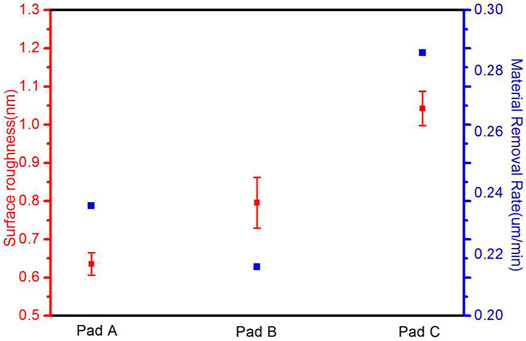
FIGURE 1. RMS roughness and MRR of GaSb wafers for the three pads.
It is well known that the polishing pad has a significant effect on the surface quality of wafers processed by CMP (Li et al., 1995). The surface layers of the three polishing pads are made of the same type of polyurethane with no grooving, but have different microporous structures.
The SEM images of the surfaces and cross-sections of the three polishing pads are shown in Figure 2. Pads A and B consist of double layers, whereas pad C has a triple-layer structure. The pore size, pore density, velvet length, thickness, compressibility and hardness of the polishing pads are listed in Table 2. Comparison of different pads under the same polishing conditions shows that the MRR of the GaSb wafers is a function of the pad surface characteristics. During polishing, the pad is under shear stress and the mechanical properties typically drop significantly with increasing pore size. The pores on the pad surface aid in transport of the polishing solution to all parts of the wafer, thereby ensuring chemical erosion and abrasive transport. When the size of the pores is larger, the solution transport capacity is also stronger. Furthermore, a low modulus of elasticity can be inferred from low compressibility of the polishing pad, leading to a reduction in the MRR. Therefore, pad C with a pore size of 45–83 µm and compressibility of 18% was found to have a higher MRR.
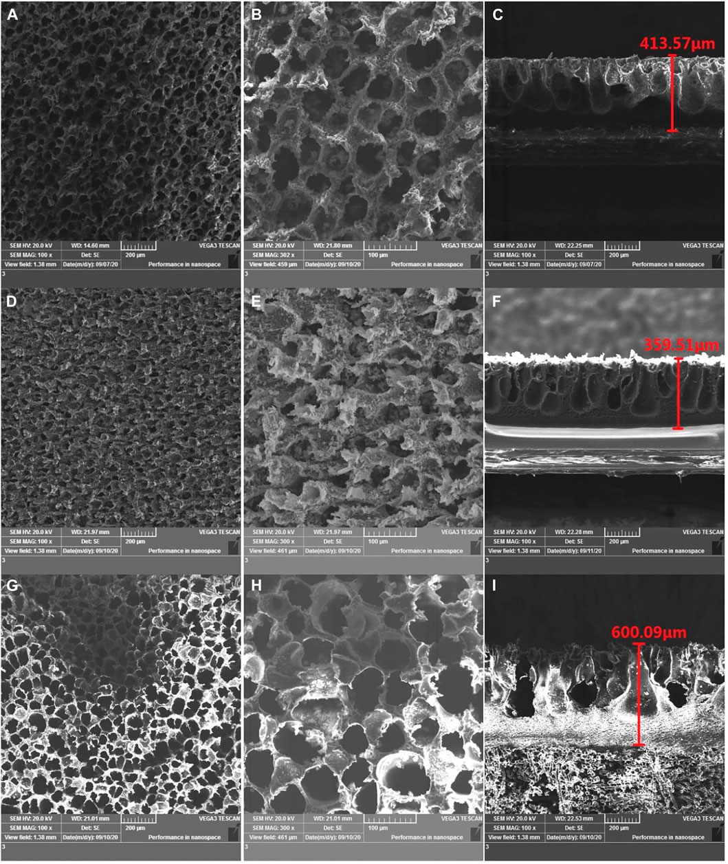
FIGURE 2. SEM morphology images of the three polishing pads: (A) plane and (C) cross-sectional views of pad A; (D) plane and (F) cross-sectional views of pad B; (G) plane and (I) cross-sectional views of pad C. (B), (E) and (H) are the enlarged views marked with the typical pore sizes for pads A, B, and C, respectively.
TABLE 2. Performances of polishing pads.
Conversely, the harder the polishing pad, the more difficult it is for the GaSb wafers to run in with the polishing pad. Thus, non-uniform surface removal caused by non-uniform friction results in lower surface quality and the RMS roughness values for multi-point tests are more widely distributed (Lee et al., 2013). Although the MRR value for pad B is low, owing to the high hardness, the roughness is greater than for pad A and the RMS roughness values measured have a narrower distribution. Therefore, pad A is judged to be a suitable pad for polishing of GaSb wafers.
Effect of Polishing Solution
The subsequent experiments of the polishing process were carried out on pad A with a polishing time of 45 min. The RMS roughness of the GaSb wafers varies with the dilution ratio of the polishing solution, as depicted in Figure 3. When the dilution ratio is 1:3, the mean RMS roughness value is 0.855 nm (based on a large scan area of 63 × 48 μm) and the MRR value is 0.597 μm/min. When the dilution ratio is 1:20, the mean RMS roughness is 0.4244 nm (based on a large scan area of 63 × 48 μm) and the MRR is 0.216 μm/min. It has been reported that the RMS roughness of wafers is reduced from 0.722–0.966 to 0.345–0.465 nm and can be considered a suitable range (Allen et al., 2011; Allen et al., 2012b).Figure 4 demonstrates the surface morphology (63 × 48 μm) of GaSb wafers polished using different dilution ratios for the polishing solution. It is evident that the morphology of the GaSb wafer surface is improved by increasing the dilution ratio of the polishing solution. Different degrees of deep scratches are apparent on wafers subjected to polishing with dilution ratios of 1:3, 1:7 and 1:10. For a dilution ratio of 1:20, the degree of deep scratches reduced, but small amounts of shallow scratches could still be observed via AFM, as shown in Figure 5.
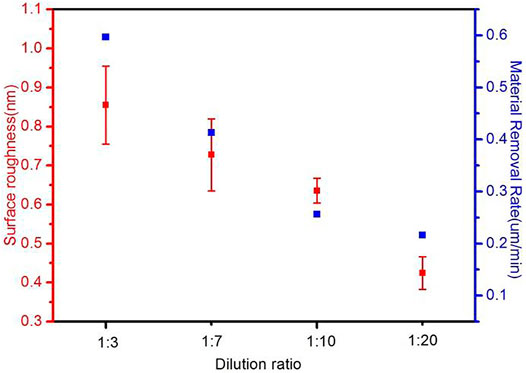
FIGURE 3. RMS roughness and MRR of GaSb wafers as a function of the dilution ratio of the polishing solution.
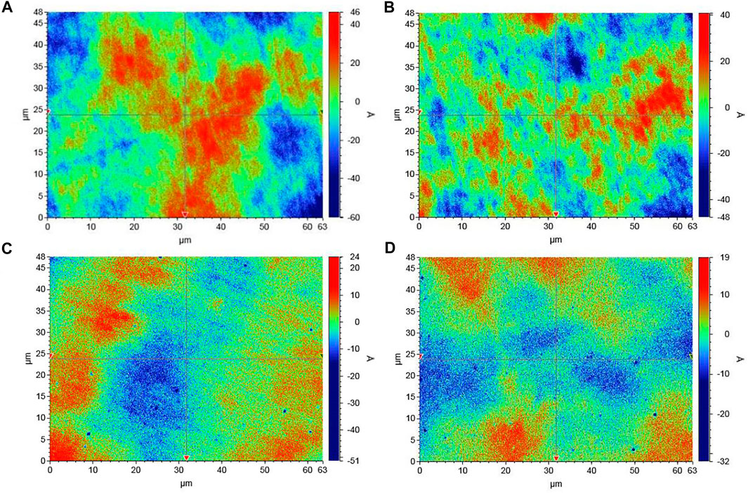
FIGURE 4. WLI morphology images of GaSb wafers under the polishing solution with dilution ratios of (A) 1:3, (B) 1:7, (C) 1:10 and (D) 1:20.
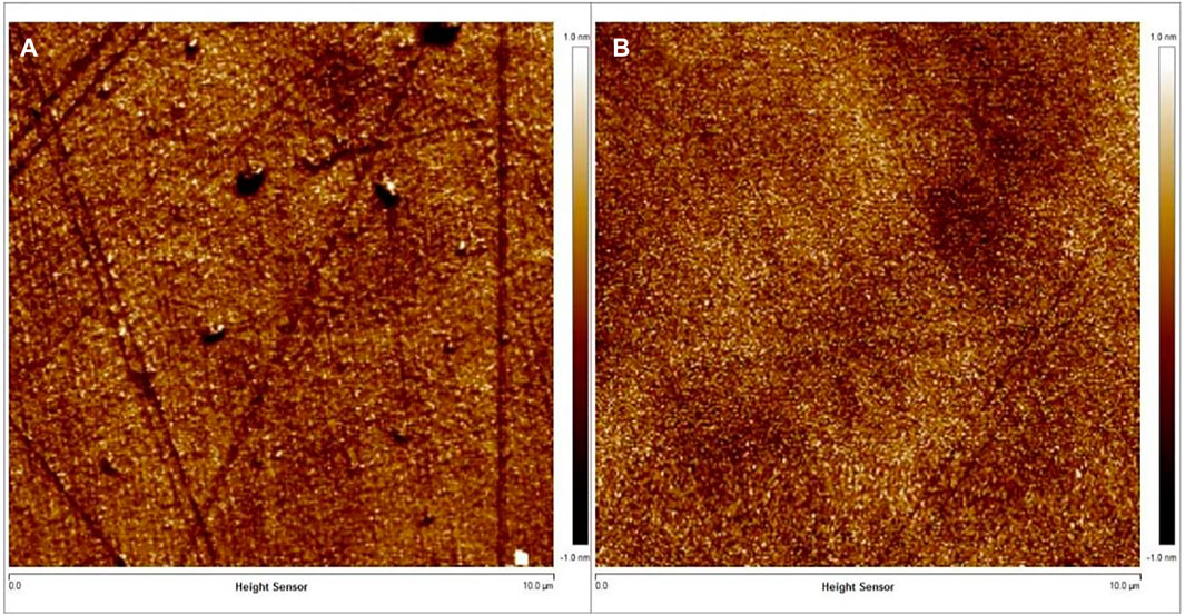
FIGURE 5. AFM images of GaSb wafers under the polishing solution with dilution ratios of (A) 1:3 and (B) 1:20.
The polishing solution mainly contains abrasive particles and oxidant. SDIC was used as the oxidant in this experiment. The oxidant can be hydrolyzed in aqueous solution via the following hydrolytic reaction:
Under the condition of the aqueous solution containing ClO−, the oxidation reaction of GaSb can be represented by the following processes (Bermudez, 2013):
For a given applied stress and polishing pad, the MRR is primarily a function of the nature of the polishing solution. With increasing dilution ratio of the polishing solution, the surface oxidation rate and abrasive concentration decrease, which lead to a reduction in the chemical and mechanical action. At a dilution ratio of 1:20, the mechanical and chemical action becomes more appropriate and results in gradual optimization of the RMS roughness of the GaSb wafer and decreasing MRR. The number of abrasive particles deposited on the surface of the polishing pad is another factor that controls the removal rate. Excess abrasives lead to a large MRR for the GaSb wafer surface, and settling of excess abrasives on the surface of the polishing pad may scratch the wafer surface (Xie et al., 1996). With increasing dilution ratio of the polishing solution, the MRR decreases from 0.597 to 0.216 μm/min and scratch levels on the GaSb wafer surface are weakened and reduce in number.
Effect of Polishing Time
It is noteworthy that the polishing time also significantly affects the surface quality of GaSb wafers. As shown in Figure 6A, the wafer RMS roughness decreases sharply to 0.41 nm (63 × 48 μm) as the polishing time increases from 0 to 40 min, and then remains nearly constant. Similarly, the MRR value decreases obviously from 1.2 to 0.159 μm/min and is then maintained at 0.16 μm/min from 40 to 150 min. Figure 6B shows the wafer PV value measured by laser interferometry, which decreases from 6.77 to 5.06 µm as the polishing time increases from 0 to 50 min. Subsequently, with increasing polishing time the wafer PV deteriorates obviously and increases up to 8.43 µm with a polishing time of 150 min. It can be concluded that 50 min is the optimum polishing time for planarization of GaSb wafers. Figure 7 demonstrates surface WLI images (63 × 48 μm) of a polished GaSb wafer surface for different polishing times. The grinding grain on the GaSb wafer surface gradually flattens out and disappears. For a polishing time of 50 min, the surface of the wafers shows low RMS roughness and no obvious deep scratches. The wafer surface then remains stable over time.
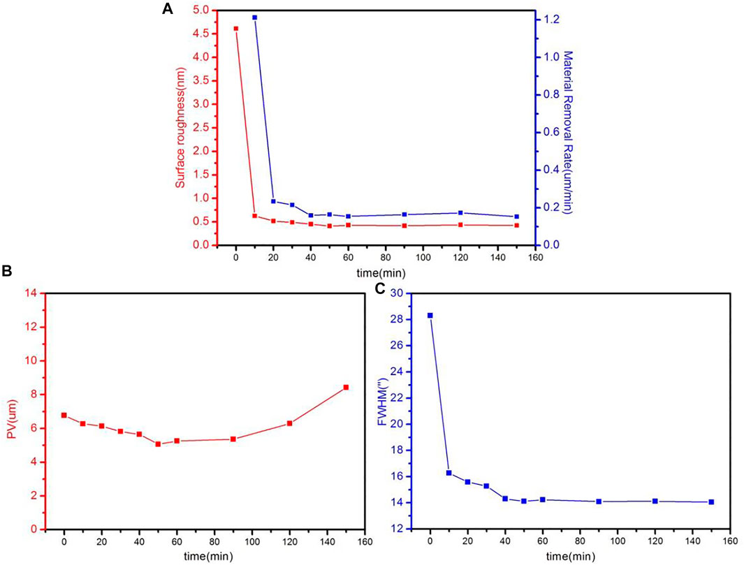
FIGURE 6. RMS roughness, MRR, PV and FWHM of GaSb wafers as a function of the polishing time.
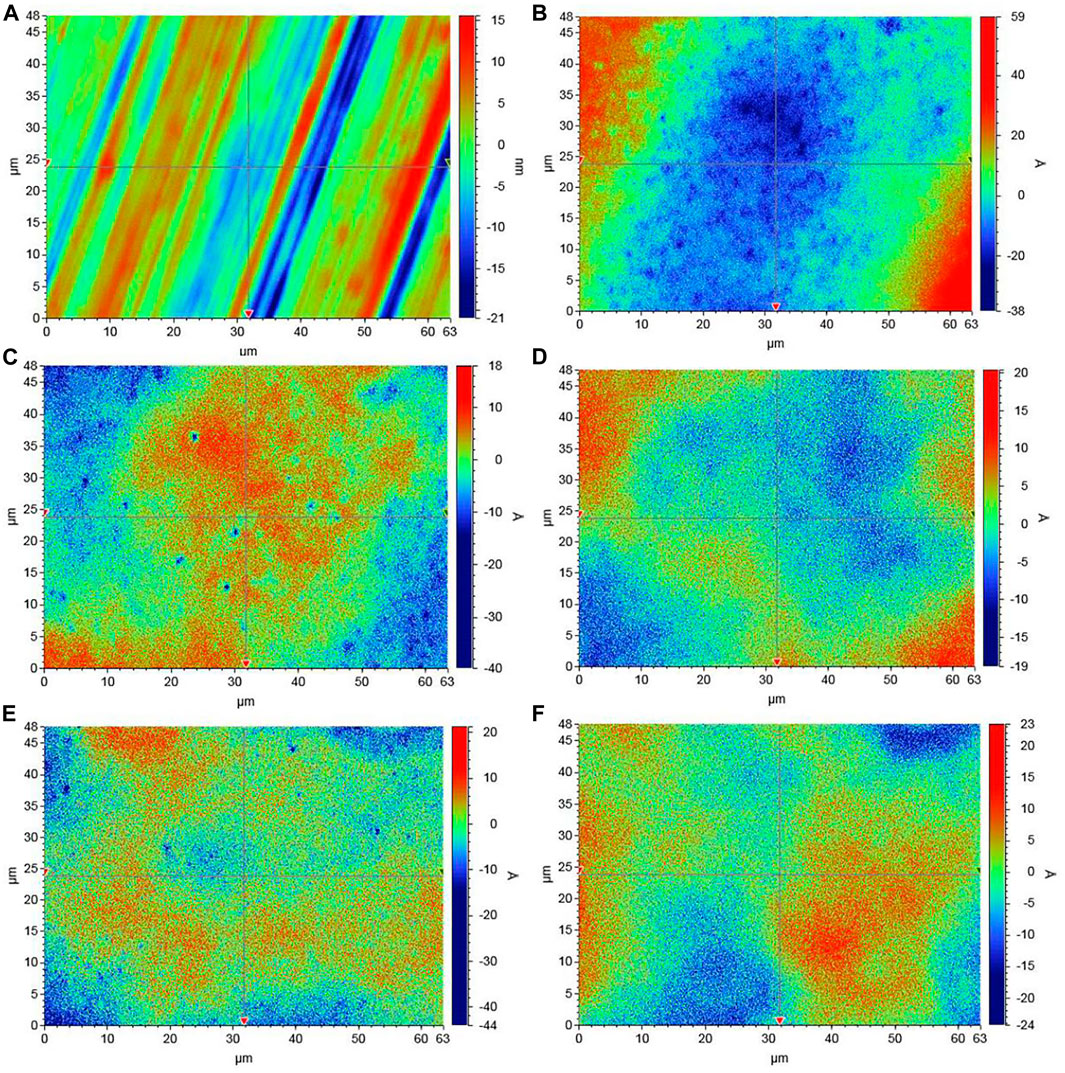
FIGURE 7. WLI images of GaSb surface with polishing times of. (A) 0, (B) 20, (C) 50, (D) 90, (E) 120 and (F) 150 min.
Figure 6C shows that the full-width half-maximum (FWHM) value for the Bragg diffraction peak of GaSb exhibits a decreasing trend, which is consistent with the RMS roughness and MRR. The FWHM value decreases from 28” to 14.3” with a polishing time of 40 min and is then maintained at this value. FWHM values can be used to characterize damage on the GaSb surface. In the early stage of polishing, initial crystalline damage to the GaSb surface is serious and surfaces are more susceptible to oxidation. Before a polishing time of 40 min, surface crystalline damage on the GaSb is easy to remove via polishing, resulting in high RMS roughness and fast MRR. After a polishing time of 40 min, surface damage on the GaSb is completely removed under certain polishing solution and pad conditions, and the RMS roughness and MRR of the GaSb wafers both reach a stable level. Figure 8 demonstrates surface WLI images (63 × 48 μm) of GaSb wafers polished using different polishing times. The GaSb wafers surface of the grinding grain disappears and flatten out gradually. For a polishing time of 50 min, the wafer surface shows low RMS roughness and no obvious deep scratches. The surface of the wafer then remains stable over time. This indicates that 50 min is the optimum polishing time for planarization of GaSb wafers.
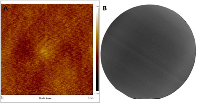
FIGURE 8. (A) AFM and (B) XRT morphology images of a GaSb surface.
Effect of pH Buffer
Since the SDIC oxidant used in the polishing solution reaches a hydrolytic equilibrium, the HClO concentration in the aqueous solution is dynamic. The chemical reaction is as follows. With the consumption of ClO− in the polishing process, the balance constantly shifts to the right and H+ is slowly released. The pH environment of the polishing solution then changes, leading to a non-ideal polishing effect. In this regard, NaHCO3 can serve as a pH buffer to stabilize the pH environment of the polishing solution by reacting with H+ and to a certain extent optimizes the stability of the chemical oxidation action.
The polishing process was conducted with a polishing solution (its dilution ratio is 1:20), a 2 wt% NaHCO3 additive and a polishing time of 50 min. Figure 7A presents the AFM image of the GaSb wafers, showing a well-controlled surface without scratches. The RMS roughness of the polished wafers can be controlled to less than 0.13 nm, indicating a better quality than that of state-of-the-art GaSb wafers available on the market (Allen et al., 2011; Allen et al., 2012b). To further evaluate the crystalline quality of the GaSb wafers, a mapping image was taken using the XRT (Wang and Matyi, 1992), which has a high resolution for crystalline defects and strain resulting from the CMP process, as shown in Figure 7B. The polished wafers show a uniform surface without obvious damage, defects or strain, indicating their high surface quality.
MBE Growth of GaSb Buffer
To further verify the quality of the polished GaSb wafers, an “epi-ready” GaSb substrate was prepared for buffer layer growth via MBE. The sample was degassed at 300 C for 30 min in a pretreatment chamber and then deoxidized at 540 C for 10 min in the reactor before growth. A buffer layer with a thickness of 1 μm was grown at 520 C. The GaSb growth rate was established as 0.5 monolayer/s using reflective high-energy electron diffraction. The Ga and Sb fluxes were kept at 3.0 × 10⁻⁷ and 2.4 × 10⁻⁶ Torr, respectively, during growth of the buffer layer, which were directly measured as the beam equivalent pressure using an ion gauge under the substrate. Figures 9A,B show an AFM image and the HRXRD rocking curve of the sample, respectively. In Figure 9A, an atomically smooth surface with RMS roughness of 0.159 nm can be observed over a 10 × 10 μm scan area, revealing a well-controlled two-dimensional growth mode. In Figure 9B, the FWHM of the Bragg diffraction peak of GaSb is 14.2”, indicating very high crystalline quality of the GaSb wafers. Hence, the optimized CMP process for GaSb can meet the requirements for MBE.
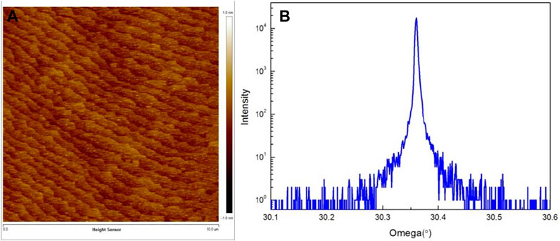
FIGURE 9. (A) AFM image and (B) HRXRD rocking curve of a GaSb buffer layer.
Conclusion
An ideal CMP process for GaSb wafers that can perform a one-pass operation for coarse and fine polishing with high quality and reliability was investigated. The MRR and RMS roughness of the GaSb wafer surface were determined as a function of the polishing pad, polishing solution, polishing time and pH buffer. With the optimum polishing condition, i.e., a polishing pad with suitable velvet properties and pore sizes, a polishing solution dilution ratio of 1:20, a polishing time of 50 min and 2 wt% NaHCO3 additive as the pH buffer, the GaSb polished wafers showed good surface morphology and structural qualities via AFM, RMS roughness of less than 0.13 nm, a scratch-free and atomically smooth surface, uniform XRT images and a perfect GaSb buffer layer grown via MBE.
Data Availability Statement
The datasets presented in this study can be found in online repositories. The names of the repository/repositories and accession number(s) can be found below: https://figshare.com/s/9229d57072a26684cf50
Author Contributions
BY, LH, contributed to conception and design of the study. HL, BZ organized the database. BY, YL performed the statistical analysis. BY wrote the first draft of the manuscript. WL, WY sections of the manuscript. All authors contributed to manuscript revision, read, and approved the submitted version.
Funding
This study received funding from Wuhan Global Sensor Technology Co., Ltd. The funder was not involved in the study design, collection, analysis or interpretation of data, the writing of this article or the decision to submit it for publication. All authors declare no other competing interests.
Conflict of Interest
All authors are employed by Wuhan Global Sensor Technology Co., Ltd.
Publisher’s Note
All claims expressed in this article are solely those of the authors and do not necessarily represent those of their affiliated organizations, or those of the publisher, the editors and the reviewers. Any product that may be evaluated in this article, or claim that may be made by its manufacturer, is not guaranteed or endorsed by the publisher.
Acknowledgments
This work was supported by Wuhan Global Sensor Technology Co., Ltd. The authors would like to thank the Global R&D team who are dedicated to valuable work and good cooperation. We are also thankful to our colleagues who greatly assisted the research.
References
Allen, L. P., Flint, J. P., Meschew, G., Dallas, G., and Bakken, D. (2011). 100mm Diameter GaSb substrates with extended IR wavelength for advanced space based applications. Proc. SPIE 8012, 801215–801222. doi:10.1117/12.882937
Allen, L. P., Flint, J. P., Meshew, G., and Trevethan, J. (2012). Surface chemistry improvement of 100mm GaSb for advanced space based applications. Proc. SPIE 8268, 826819–826821. doi:10.1117/12.904778
Allen, L. P., Flint, J. P., Meshew, G., Trevethan, J., Dallas, G., Khoshakhlagh, A., et al. (2012). Manufacturing of 100mm diameter GaSb substrates for advanced space based applications. Proc. SPIE 8268, 826817–826821. doi:10.1117/12.904777
Bajaj, R. M., Desai, M., Stell, M., and Tolles, R. (1994). Effect of Polishing Pad Material Properties on Chemical Mechanical Polishing (Cmp) Processes. Mater. Res. Soc. Symp. Proc., 337. doi:10.1557/PROC-337-637
Bermudez, V. M. (2013). The Effects of the Initial Stages of Native-Oxide Formation on the Surface Properties of GaSb (001). J. Appl. Phys. 114 (2), 024903. doi:10.1063/1.4812740
Dutta, P. S., Bhat, H. L., and Kumar, V. (1997). The Physics and Technology of Gallium Antimonide: An Emerging Optoelectronic Material. J. Appl. Phys. 81 (9), 5821–5870. doi:10.1063/1.365356
Hooper, B. J., Byrne, G., and Galligan, S. (2002). Pad Conditioning in Chemical Mechanical Polishing. J. Mater. Process. Tech. 123, 107–113. doi:10.1016/s0924-0136(01)01137-2
Krishnaswami, K., Vangala, S. R., Dauplaise, H. M., Allen, L. P., Dallas, G., Bakken, D., et al. (2008). Molecular Beam Epitaxy on Gas Cluster Ion Beam-Prepared GaSb Substrates: Towards Improved Surfaces and Interfaces. J. Cryst. Growth 310, 1619–1626. doi:10.1016/j.jcrysgro.2007.11.225
Lee, E.-S., Cha, J.-W., and Kim, S.-H. (2013). Evaluation of the Wafer Polishing Pad Capacity and Lifetime in the Machining of Reliable Elevations. Int. J. Machine Tools Manufacture 66, 82–94. doi:10.1016/j.ijmachtools.2012.11.003
Li, W., Shin, D. W., Tomozawa, M., and Murarka, S. P. (1995). The Effect of the Polishing Pad Treatments on the Chemical-Mechanical Polishing of SiO2 Films. Thin Solid Films 270, 601–606. doi:10.1016/0040-6090(96)80082-4
Liu, A. W. K., Lubyshev, D., Qiu, Y., Fastenau, J. M., Wu, Y., Furlong, M. J., et al. (2015). MBE Growth of Sb-based Bulk nBn Infrared Photodetector Structures on 6-inch GaSb Substrates. Proc. SPIE 9451, 94510T–1. doi:10.1117/12.2178122
Liu, Z. Y., Hawkins, B., and Kuech, T. F. (2003). Chemical and Structural Characterization of GaSb(100) Surfaces Treated by HCl-Based Solutions and Annealed in Vacuum. J. Vac. Sci. Technol. B 21 (1), 71–77. doi:10.1116/1.1532023
Martinez, R., Amirhaghi, S., Smith, B., Mowbray, A., and Furlong, M. J. (2012). Large Diameter Ultra-flat Epitaxy Ready GaSb Substrates: Requirements for MBE Grown Advanced Infrared Detectors. Proc. SPIE 8353, 835314–835322. doi:10.1117/12.919777
Rogalski, A., Antoszewski, J., and Faraone, L. (2009). Third-generation Infrared Photodetector Arrays. J. Appl. Phys. 105, 091101. doi:10.1063/1.3099572
Wang, V. S., and Matyi, R. J. (1992). Triple crystal X‐ray Diffraction Analysis of Chemical‐mechanical Polished Gallium Arsenide. J. Appl. Phys. 72, 5158–5164. doi:10.1063/1.351995
Keywords: GaSb, polishing pad, dilution ratio, pH buffer, root mean square (RMS) roughness, molecular beam epitaxy
Citation: Yan B, Liang H, Liu Y, Liu W, Yuan W, Zhang B and Huang L (2021) Chemical Mechanical Polishing of GaSb Wafers for Significantly Improved Surface Quality. Front. Mater. 8:773131. doi: 10.3389/fmats.2021.773131
Received: 09 September 2021; Accepted: 30 September 2021;
Published: 18 October 2021.
Edited by:
Jijie Huang, Sun Yat-sen University, ChinaCopyright © 2021 Yan, Liang, Liu, Liu, Yuan, Zhang and Huang. This is an open-access article distributed under the terms of the Creative Commons Attribution License (CC BY). The use, distribution or reproduction in other forums is permitted, provided the original author(s) and the copyright owner(s) are credited and that the original publication in this journal is cited, in accordance with accepted academic practice. No use, distribution or reproduction is permitted which does not comply with these terms.
*Correspondence: Li Huang, Z3VpZGVobEAxNjMuY29t