 Tenghui Ouyang
 Ximiao Wang
 Shaojing Liu
 Huanjun Chen
94% of researchers rate our articles as excellent or good
Learn more about the work of our research integrity team to safeguard the quality of each article we publish.
Find out more
ORIGINAL RESEARCH article
Front. Mater., 30 July 2021
Sec. Semiconducting Materials and Devices
Volume 8 - 2021 | https://doi.org/10.3389/fmats.2021.736180
This article is part of the Research TopicSpotlight on China - Materials ScienceView all 14 articles
Two-dimensional (2D)-material-based photodetectors have recently received great attention due to their potentials in developing ultrathin and highly compact devices. Avalanche photodiodes (APDs) are widely used in a variety of fields such as optical communications and bioimaging due to their fast responses and high sensitivities. However, conventional APDs based on bulk materials are limited by their relatively high dark current. One solution to tackle this issue is by employing nanomaterials and nanostructures as the active layers for APDs. In this study, we proposed and fabricated an atomically-thick APD based on heterojunctions formed by 2D transition metal dichalcogenides (TMDs). A typical device structure was formed by stacking a semiconducting monolayer WS2 onto two metallic few-layer MoTe2 flakes. Due to the Schottky barrier formed between the TMD layers and their atomic thicknesses, the dark current of the APD is greatly reduced down to 93 pA. In addition, the APD can operate through a broad spectral range from visible to near-infrared region, with a responsivity of 6.02 A/W, an external quantum efficiency of 1,406%, and an avalanche gain of 587. We believe that the 2D APD demonstrated here provides a feasible approach for developing all-2D optoelectronic devices with simultaneous high-sensitivity and low noise.
2D atomic crystals have attracted extensive interests during the past decade due to their excellent electrical, optical, and optoelectronic properties. Echo with their ultrathin structure, a broad range of potential applications can be envisioned, including high-performance 2D transistors (Yoon et al., 2013; Liu et al., 2015; Choi et al., 2016; Chuang et al., 2016; Liu et al., 2019; Zheng et al., 2020), photodetectors (Mittendorff et al., 2013; Cheng et al., 2014; Mudd et al., 2015; Tao et al., 2015; Wang et al., 2015; Shim et al., 2016; Vu et al., 2017; Yu et al., 2017; Zeng et al., 2019; Wang et al., 2020), ultra-compact and flexible light-emitting diodes (Withers et al., 2015; Wang et al., 2017; Shang et al., 2018), sensors (Burman et al., 2016; Shokri and Salami, 2016; Guo et al., 2017), to name but a few. In particular, 2D transition metal dichalcogneides (TMDs) are usually semiconductors with exotic characteristics which can open up new avenues for both of fundamental research and practical applications. For example, monolayer WS2 is shown to be a direct bandgap semiconductor with strong room-temperature exciton binding energy. It has been widely employed as quantum emitters for studying of strong light−matter interactions in different types of micro- and nanocavities (Wen et al., 2017). In addition, monolayer WS2 exhibits strong absorption across the visible spectral range, as well as excellent chemical stability (Bernardi et al., 2013; Zhang et al., 2013). These allow it to act as active layers for photodetectors. The few-layer MoTe2 is reported to be a type-II Weyl semimetal, which can be employed as electrodes in the 2D devices for its high carrier mobility and good electric conduvtivity (Zhang et al., 2014; Beams et al., 2016; Chen et al., 2016). Furthermore, one can also explore new physical phenomena associated with the semimetal phase in the few-layer MoTe2 (Keum et al., 2015).
Avalanche photodiodes (APDs), which consist of p−n junctions or Schottky junctions, are able to convert the incoming photons into charge carriers undergoing cascade amplifications upon reverse bias (Johnson, 1965; Anderson and McMurtry, 1966; Aull et al., 2002). When operating in the avalanche regime, APDs can exhibit high internal gain for photodetection of ultrahigh sensitivity, making them widely used in optical communications (Liu et al., 1992; Ferraro et al., 2015), single-photon detection (Huntington et al., 2007; Faramarzpour et al., 2008; Ren et al., 2011), and bioimaging (Vo-Dinh et al., 2010; Wohnhaas et al., 2013). However, conventional APDs based on bulk materials are usually limited by their relatively high dark current. This issue can be alleviated by reducing the volume of the devices, which is typically accompanied by sacrifice of device responsivity and quantum efficiency. During the past decade, due to their atomic thicknesses, strong optical absorption, and high photocurrent conversion efficiencies, 2D crystals have been demonstrated to provide a new avenue for developing high-performance photodetectors with low dark current and high responsivity (Table 1).
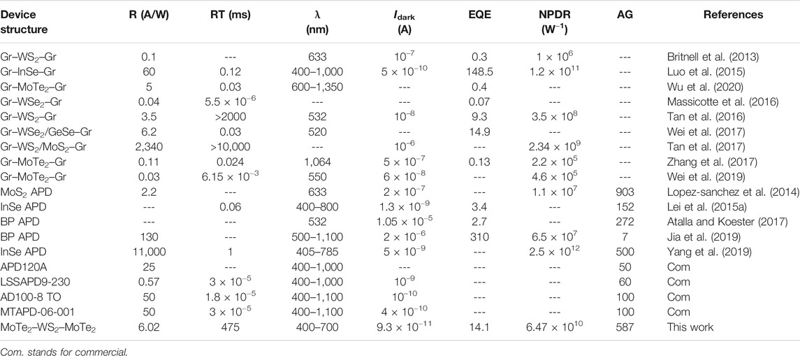
TABLE 1. Comparison of device performances.
Generally, in 2D photodetectors bulk metals such as titanium and gold are utilized as electrodes. A limitation of these electrodes is that acquiring defect-free interface between metal and 2D crystals without Fermi level pinning or carrier scattering is still a challenge, because defects and dangling bonds in these metal electrodes will introduce plentiful interfacial states (Gong et al., 2014; Kim et al., 2017). In contrast, the passivated and dangling-bond-free surfaces of 2D crystals can make them integrate layer-by-layer to form heterojunctions bonded through van der Waals (vdW) force. Accordingly, devices free of interface defects can be formed through stacking different types of 2D crystals. Specifically, all-2D photodetectors have been developed by respectively adopting the 2D crystals as electrodes and active layers (Britnell et al., 2013; Luo et al., 2015; Massicotte et al., 2016; Tan et al., 2016; Padilha et al., 2017; Tan et al., 2017; Wei et al., 2017; Zhang et al., 2017; Yao and Yang, 2018; Wei et al., 2019; Yang et al., 2019; Wu et al., 2020). Although these all-2D devices exhibit excellent photodetection performances, their room-temperature dark currents are still relatively high (in the range of ∼0.1 nA–1 μA, Table 1). Such high dark currents will deteriorate the signal-to-noise (S/N) ratio of the photodetectors and consequently limit the device applications in sensing of low photon flows.
In this study, we present an all-2D APD composed of a monolayer WS2 and two few-layer MoTe2 flakes (MoTe2–WS2–MoTe2 heterostructure). The metallic MoTe2 flakes act as electrodes. A Schottky barrier can thereafter be formed at the interface between the semiconducting WS2 and metallic MoTe2. Upon reverse bias, the APD is demonstrated with a responsivity (R) of 6.02 A/W, an external quantum efficiency (EQE) of 1,406%, and an avalanche gain (AG) of 587. In particular, due to the Schottky barrier, a dark current as low as 93 pA can be obtained. The R and EQE is at the forefront of the all-2D photodetectors, while the dark current is even better than many state-of-the-art commercial APDs. In addition, wavelength scanned measurements further indicated that the APD operated in a broad spectral range from 400 to 700 nm. Our results therefore demonstrate a facile approach for design and fabrication of room-temperature all-2D photodetectors with simultaneous high-sensitivity and low noise.
Monolayer WS2 was purchased from 6Carbon Technology company in China. Few-layer MoTe2 was grown on the silicon substrate covered with 300-nm-thick SiO2 layer according to the process reported previously (Chen et al., 2017).
The MoTe2–WS2–MoTe2 heterostructure was fabricated using a wet-transfer method (Wen et al., 2017). Specifically, Polystyrene (PS) was first coated on the surface of the substrate covered with monolayer WS2 flakes. Then, the substrate covered with PS film was put into water so that the PS film pasted with WS2 was stripped off from the substrate. Subsequently, the WS2 adhered onto the PS film was transferred onto two few-layer MoTe2 flakes separated with a micrometer-scale gap. After incubation at 110°C for 60 s, the sample was immersed into toluene solution for 2 hours to dissolve the PS film, whereby heterojunctions were formed between the WS2 and two MoTe2 flakes.
To fabricate the MoTe2–WS2–MoTe2 heterojunction device structure, maskless lithography (uPG501, Wavetest) was employed to pattern the two electrodes. Afterwards, titanium (Ti, 10-nm thick) and gold (Au, 100-nm thick) were deposited using an electron-beam evaporation system (DE400, Wavetest). The heterojunction device structure was obtained after the lift-off process.
Raman and photoluminescence (PL) spectra were measured using a micro-Raman spectrometer (inVia Reflex, Renishaw). The excitation laser with a wavelength of 532 nm was focused onto the samples through a ×50 objective (numerical aperture 0.80). The diameter of the focusing spot is ∼1 μm. The thicknesses of the WS2 and MoTe2 flakes were measured using an atomic force microscope (AFM, NTEGRA Spectra, NT-MDT). The photocurrents were measured by a sourcemeter (Keithley 2636B, Tektronix), with incidence wavelengths of 405, 532, 633, 785, and 1,064 nm. In addition, a supercontinuum laser source with an output wavelength range of 400–2400 nm (Fianium, SC400-4-PP) was employed to measure the photocurrent spectrum. The noise power spectra of the device under different bias voltages were collected using a semiconductor characterization system (FS-Pro™, Hongkong Base For Information Technology).
The configuration of the all-2D APD device is schematically shown in Figure 1A, which consists of a monolayer WS2 overlaid onto two few-layer MoTe2 flakes. The metallic MoTe2 flakes act as electrodes in the APD. In this way two heterojunctions were formed at the overlapped regions between the WS2 and MoTe2. Afterwards, titanium and gold layers were consecutively deposited on the MoTe2 flakes as electrodes for electrical readout. Optical microscope image of the APD is displayed in Figure 1B. The channel length (i.e., separation between the two MoTe2 flakes) of the device is measured as 2 μm. The thickness of the WS2 flake is 1.0 nm, and those of the two MoTe2 flakes are 4.3 and 4.5 nm, respectively (Supplementary Figure S1, Supporting Information). The monolayer nature of the WS2 can be further confirmed by Raman spectroscopy characterizations (Figure 1C). Two strong peaks are observed at 352 cm−1 and 418 cm−1, corresponding to the 2LA(M) and A1g(Γ) modes of WS2, respectively. The peak intensity ratio of 2LA(M)/A1g(Γ) can be determined as 6.6, which is a typical feature of monolayer WS2 (Cong et al., 2014; Xu et al., 2015). For Raman spectrum collected from the MoTe2 region, a small peak at 188.91 cm−1 can be observed, which is the Bg mode of MoTe2 in 1T′ phase (Kan et al., 2015; Naylor et al., 2016; Chen et al., 2017). 1T′-MoTe2 is a semimetal and a good candidate of 2D electrode material because of its low resistance and high carrier mobility (Zhang et al., 2014; Beams et al., 2016; Chen et al., 2016). Due to its strong exciton transition at room temperature, the pristine monolayer WS2 exhibits a strong PL peak at 614 nm (Figure 1D). In contrast, because of its semimetal nature, negligible PL signal can be observed in the 1T′-MoTe2 region. It is noted that in the heterostructure regions both the Raman and PL signals from WS2 are reduced (Figures 1C,D). Such a phenomenon suggests intimate contact between the monolayer WS2 and few-layer MoTe2. Once the intimate contact is formed, the WS2 excitons or lattice vibrations will transfer their energies to the MoTe2 underneath through electromagnetic coupling. Subsequently, the lattice vibration energy or exciton energy will be dissipated by the impurities, defects, and free electrons in the semimetal layer. As a result, the Raman and PL signals of the WS2 will be quenched.
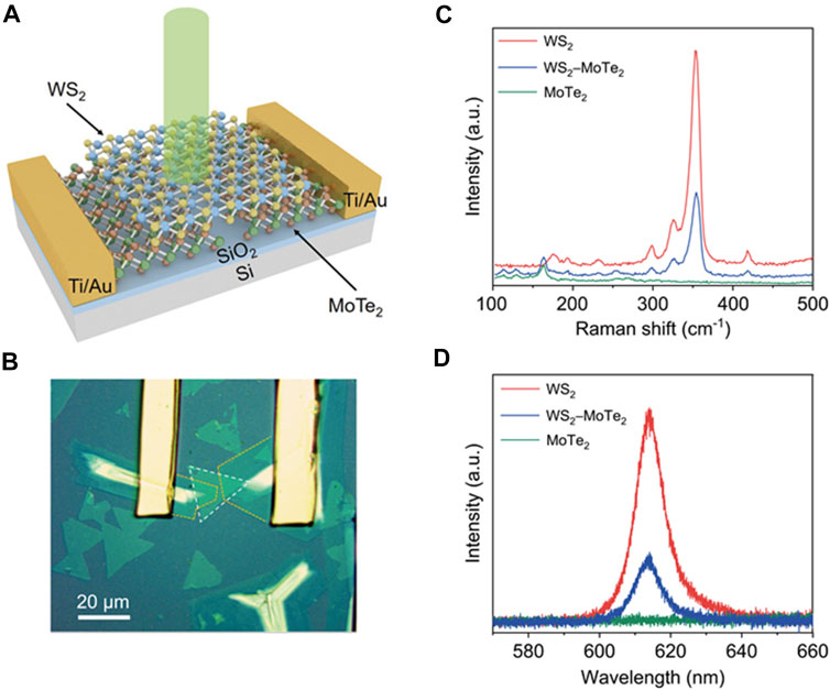
FIGURE 1. Material characterizations of the MoTe2–WS2–MoTe2 heterojunction device. (A) Schematic showing the APD composed of a monolayer WS2 flake overlaid onto two few-layer MoTe2 flakes. The green cylinder delegates the incidence light. (B) Optical microscope image of the fabricated MoTe2–WS2–MoTe2 heterostructure. The WS2 region is marked with white dashed lines. The MoTe2 regions are marked with yellow dashed lines. (C, D) Raman (C) and PL (D) spectra of the MoTe2–WS2–MoTe2 heterostructure. The spectra are collected from the monolayer WS2 (red), few-layer MoTe2 (green), and WS2–MoTe2 heterojunction (blue) regions. The excitation laser is of 532-nm wavelength.
Schottky junctions can be formed at the two heterojunctions between the semiconducting WS2 and semimetal MoTe2 layer. Figure 2A shows the dependence of current on bias voltage in a representative device. Specifically, the current increases along with the increase of bias voltage and saturates at 10.4 V. Afterwards, the current increases notably when the bias is further increased. Such bias voltage dependence is typical of Schottky diodes. Due to the Schottky barrier, the device exhibits a dark current as low as 93 pA under a bias voltage of 59 V. Such a dark current is much lower than many photodetectors based on 2D materials and even lower than typical commercial APDs (Table 1). The Schottky barriers at the heterojunctions can trigger electron avalanche effect upon applying a large electrical field across the device. The current at 10.4 V (26 pA) is defined as the saturation current Isat59. Bias voltages above 10.4 V will accelerate the charge carriers passing through the heterojunction, giving rise to ionization collisions of the lattice and generation of additional charge carriers, i.e., occurrence of electron avalanche effect. To further demonstrate the avalanche effect, a charge carrier multiplication factor, M, is defined as M = I/Isat, with I the current above 10.4 V. When the avalanche effect occurs, parameter M will follow the behavior (Miller, 1957),
where n represents ionization rate, Vb is a fitting parameter. Equation (1) can be rewritten as,
suggesting a linear dependence of
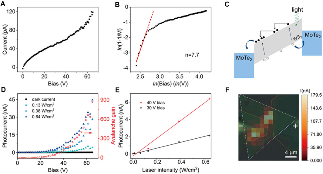
FIGURE 2. Electrical and photocurrent characterizations of the MoTe2–WS2–MoTe2 heterojunction device. (A) Dependence of dark current on bias voltage of the heterojunction device. (B) Relationship between ln(1−1/M) and ln(V). M is the multiplication factor. V is the bias voltage. Red dashed line is the linear fit. (C) Schematic showing the operation principle of the heterojunction device. (D) Photocurrent response of the MoTe2–WS2–MoTe2 heterojunction device under different light illumination intensities. Red opened circles show the corresponding AGs upon an excitation intensity of 0.64 W/cm2. The illumination wavelength is 532 nm. (E) Intensity-dependent photocurrent of the MoTe2–WS2–MoTe2 heterojunction device. The applied bias voltages are 30 V (black) and 40 V (red). (F) Photocurrent mapping of MoTe2–WS2–MoTe2 heterojunction device. White dashed lines mark out the WS2 region. Yellow solid lines mark out the MoTe2 region. Symbols “+” and “−” indicate the direction of the bias voltage.
The avalanche effect and small dark currents of the MoTe2–WS2–MoTe2 heterostructure can greatly benefit photodetection. Figure 2C illustrates the operation principle of the heterostructure APD. Electron−hole pairs will be generated in both of the 2D layers and Schottky junctions upon light illumination. When a bias voltage is applied to initiate the avalanche effect, carrier multiplications will occur, giving rise to a rapid increase of the photocurrent with the applied bias. Additionally, a larger S/N ratio will be obtained as well. Figure 2D shows the current responses of the device measured in the dark and under 532-nm laser excitations of different intensities (green: 0.13 W/cm2; cyan: 0.38 W/cm2; blue: 0.64 W/cm2). The dark current remains below 100 pA even when the bias voltage is above 60 V. In contrast, the photocurrent increases slowly with applied bias smaller than 10.4 V, then dramatically grows when the bias voltage become larger due to the avalanche effect. Moreover, the photocurrent increases against illumination intensity. By plotting the photocurrent as a function of the laser intensity, linear dependences can be observed at two typical bias voltages (30 and 40 V, Figure 2E) for laser intensity upto 0.64/cm2.
R, EQE, and AG are three important parameters evaluating the performance of an APD. Specifically, R, EQE, and AG can be calculated according to the following formulae (Yu et al., 2013; Long et al., 2019),
where Iph, Idark, and Pin represent photocurrent, dark current, and incidence light intensity, respectively. Parameter h is the Planck constant (h = 6.62607015 × 10⁻³⁴ J s), c is the speed of light (c = 2.99792458 × 10⁸ m/s), e is quantity of a unit electric charge (e = 1.602176634 × 10⁻¹⁹ C), λ is wavelength of incidence light. Parameters Iph0 and Idark0 are the photocurrent and dark current before the occurrence of avalanche effect, respectively. In our analyses, Iph0 and Idark0 were taken at the bias of 10.4 V.
We evaluate the R, EQE, and AG of the heterojunction device with an illumination intensity of 0.64 W/cm2. As shown in Figure 2D, the AG increases distinctly as a function of the bias voltage. At a bias of 59 V, the R and EQE are calculated to be 6.02 A/W and 1,406%, respectively, corresponding to an AG of 587. Table 1 summarizes the performances of various 2D photodetectors, including APD and non-APD types, as well as typical APDs that are commercially available. It is seen that although the R of the MoTe2–WS2–MoTe2 heterojunction device is moderate, its EQE and AG are among the best ones. In particular, the AG of the heterojunction device is much better than the listed commercial APDs can exhibit. Moreover, the dark current of our device is merely 93 pA at a bias of 59 V, which is at the lowest level among both of the 2D and commercial photodetectors. The normalized photocurrent-to-dark current ratio (NPDR) can be further calculated as NPDR = R/Idark = 6.47 × 10¹⁰ W−1, which is better than most of the 2D photodetectors can provide (Table 1). These results suggest that our 2D APD can provide an excellent S/N ratio and favor the detection of low-level signals.
Figure 2F shows a typical 2D photocurrent map of the MoTe2–WS2–MoTe2 heterojunction APD. To avoid electrical breakdown of the device, a relatively small voltage of 25 V is applied to reversely bias the left Schottky junction. According to Figure 2A, such a bias can already trigger the avalanche effect. In addition, to induce strong enough photocurrent for the 2D mapping, a relatively large incidence intensity of 305.73 W/cm2 was used. As shown in Figure 2F, photocurrent was visible near the left Schottky junction (reversely bias) and the channel region. However, negligible photocurrent can be found at the right Schottky junction which is forward biased. These observations can be understood by considering that in the avalanche regime, the photocurrent is proportional the magnitude of collision ionization. The photo-generated electrons in the reversely-biased Schottky junction and regions nearby will experience a longer acceleration path, which will therefore undergo more collision events. These additional collisions will generate more electrons, giving rise to stronger photocurrents.
Figure 3A illustrates the switching characteristic of the broadband photoresponse of MoTe2–WS2–MoTe2 heterojunction APD under a bias voltage of 50 V at 532-nm excitation. The three ON/OFF cycles are similar with each other, suggesting that photodetection performance of our APD is repeatable. Response time (RT), which is another important parameter characterizing a photodetector, can be deduced from one typical cycle. As shown in Figure 3B, the RTs are revealed as 1,260 and 475 ms for the laser-on and–off processes, respectively. As an APD, the RTs of our heterojunction photodetector is ordinary among the 2D photodetectors (Table 1). The origin of such long RTs can be possibly due to introduction of carrier trapping centers during the device manufacturing processes. It is known that impurities and defects will be generated at the interface of the heterojunction by stacking different 2D materials via wet-transfer method (Rooney et al., 2017). These impurities and defects will act as trapping states for electrons and holes, which will increase the photocurrent gain but largely compromise the RT of the photodetectors (Hu et al., 2012; Lopez-Sanchez et al., 2013; Lei et al., 2015a; Lei et al., 2015b). To fasten the device responses, improvement of the device manufacturing processes is required.
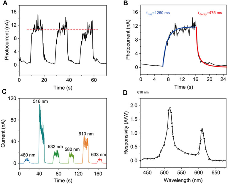
FIGURE 3. Time- and spectrum-resolved photoresponses of the MoTe2–WS2–MoTe2 heterojunction device. (A) Photocurrents of the device in response to three ON/OFF illumination cycles. The red dashed line suggests that the photocurrent maxima of the three cycles are the same. (B) Photocurrent of the device during one typical ON/OFF illumination cycle. Blue and red curves are fitting results by assuming that the rise and decay processes of the photocurrent are exponential dependences. (C) Representative switching behaviors of the heterojunction device under illuminations at 480, 516, 532, 580, 610, and 633 nm. (D) Photocurrent spectrum of the heterojunction device.
We further study the broadband photocurrent performance of the MoTe2–WS2–MoTe2 APD by illuminating the device at different wavelengths. To that end, the bias voltage was fixed at 30 V, the laser spot was focused onto the center of the left Schottky junction shown in Figure 2F. The incidence wavelength was selected by placing a specific narrowband optical filter in front of the exit of the supercontinuum laser. Representative switching behaviors of the APD illuminated at 480, 516, 532, 580, 610, and 633 nm are shown in Figure 3C. The device exhibits similar ON/OFF behaviors and same dark currents at different excitation wavelengths. Moreover, two clear photocurrent maxima were observed at 516 and 610 nm, respectively. This can be seen more clearly by plotting the R against illumination wavelength, i.e., the photocurrent spectrum (Figure 3D). The peak at 610 nm should correspond to the exciton-A transition in the monolayer WS2, as corroborated with the PL spectrum shown in Figure 1D. The peak at 516 nm with a larger R can be ascribed to exciton-B in monolayer WS2. The separation between the two photocurrent maxima is 0.37 eV, which is consistent with the splitting energy of the valence band minimum in WS2 arising from the spin-orbit coupling at K (K′) valley (Zeng et al., 2013; Zhao et al., 2013; Zhu et al., 2015). Previous studies have demonstrated that the recombination rate of exciton-B is much smaller than that of exciton-A, giving rise to a much lower PL quantum yield of exciton-B (Zeng et al., 2013; Zhao et al., 2013; Zhu et al., 2015). Accordingly, more photo-generated carriers will undergo avalanche multiplications under optical excitation associated with exciton-B, leading to a stronger photocurrent response. Another important observation is that the photocurrent response can extend to wavelengths larger than 614 nm, i.e., the exciton transition energy of WS2. Such an effect can be ascribed to photo-generated electron transmitting over the Schottky barrier from the Fermi energy of the metallic MoTe259. On the basis of the photocurrent spectrum shown in Figure 3D, the Schottky barrier height can be extracted as 1.93 eV (Supplementary Figure S2, Supporting Information), corresponding to a wavelength of 642 nm. This low Schottky barrier height guarantees photocurrent response of the APD under optical excitation with energy smaller than the exciton transition energy of the monolayer WS2.
With the knowledge of dark current, AG, RT, and M, the S/N ratio can be readily calculated according to (Lei et al., 2015a),
where BW is the bandwidth. In a specific calculation, BW is set as inverse of the RT (Lei et al., 2015a). Under an illumination intensity of 0.64 W/cm2 and a bias voltage of 59 V, the S/N ratio is calculated as 71 dB, which is 10 times larger than that of a 2D APD (60 dB) consisted of layered InSe and bulk metal electrode (Lei et al., 2015a). The enhanced S/N ratio in our device is attributed to its ultralow dark current even in the avalanche regime.
Finally, we characterized the current noise density of the MoTe2–WS2–MoTe2 APD, whereby the noise equivalent power (NEP) and normalized detectivity (D*) can be calculated. Figure 4 shows the low-frequency noise power spectra of the device under different applied bias voltages. The noise increases against the bias voltage. In addition, all of the four noise power spectra can be well fitted using the equation
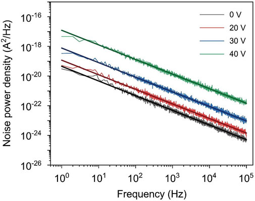
FIGURE 4. Noise power spectra of the MoTe2–WS2–MoTe2 heterojunction APD under different applied bias voltages. The black straight lines are linear fittings of the noise power spectra under different bias voltages.
By integrating Sn(f) within a given bandwidth B (usually B is set as 1 Hz), the total noise current power can be expressed as (Chang et al., 2011),
The NEP and D* can thereafter be obtained as (Chang et al., 2011),
where A is the effective APD area used to normalized the noise, which is 294 μm2 according to the triangular WS2 region shown in Figure 1B. Parameter B is the test bandwidth which is set as 100 kHz. Therefore, for a bias voltage of 40 V, the corresponding NEP and D* are calculated as 7.49 × 10⁻¹¹ W/Hz0.5 and 7.24 × 10⁹ Jones, respectively.
In summary, we successfully demonstrate an all-2D APD structure with ultralow dark current. By stacking a monolayer semiconducting WS2 onto two few-layer semimetal MoTe2 flakes, two back-to-back Schottky barriers were formed at the two heterojunctions between the WS2 and MoTe2. Due to the double Schottky barriers and good crystallinity of the 2D crystals, the fabricated device structure can exhibit excellent electrical avalanche effect. When operating in the avalanche regime, the heterojunction structure can act as an APD with improved photodetection performances and a remarkably low dark current. The EQE of our APD is 1,406%, with an AG of 587 and dark current as low as 93 pA. Moreover, due to the small Schottky barrier height, the 2D APD can operate in a broadband spectrum range from 400 to 700 nm. Further optimization of the APD performances is possible. For example, by selecting 2D crystals with favorable energy band structures and alignments, it is possible to establish proper Schottky barriers to further minimize the dark currents and expand the operation wavelength ranges. Additionally, by improving the processing techniques of the 2D stacked heterostructures, one can reduce the RT and current noise. We therefore believe that the results obtain in the current study can pave the way for design and fabrication of miniaturized all-2D optoelectronic devices with supreme performances.
The original contributions presented in the study are included in the article/Supplementary Material, further inquiries can be directed to the corresponding author.
HC and SD conceived the study and supervised the project. TO fabricated the all-2D APD device and characterized the device performances. XW and SL helped prepare the samples and characterizations. TO, XW, SL, HC, and SD analyzed the data and discussed the results. The manuscript was written through contributions of all authors. All authors have given approval to the final version of the manuscript.
We acknowledge support from the National Key Basic Research Program of China (grant no. 2019YFA0210203), the National Natural Science Foundation of China (grant nos. 91963205 and 11904420), Guangdong Basic and Applied Basic Research Foundation (grant no. 2020A1515011329). HC acknowledges the support from Changjiang Young Scholar Program.
The authors declare that the research was conducted in the absence of any commercial or financial relationships that could be construed as a potential conflict of interest.
The reviewer LS declared a past co-authorship with one of the authors HC to the handling Editor.
All claims expressed in this article are solely those of the authors and do not necessarily represent those of their affiliated organizations, or those of the publisher, the editors and the reviewers. Any product that may be evaluated in this article, or claim that may be made by its manufacturer, is not guaranteed or endorsed by the publisher.
The Supplementary Material for this article can be found online at: https://www.frontiersin.org/articles/10.3389/fmats.2021.736180/full#supplementary-material
Anderson, L. K., and McMurtry, B. J. (1966). High-Speed Photodetectors. Proc. IEEE 54 (10), 1335–1349. doi:10.1109/proc.1966.5121
Atalla, M. R. M., and Koester, S. J. (2017). “Black Phosphorus Avalanche Photodetector,” in 75th Annual Device Research Conference (DRC), South Bend, IN, June 25–28, 2017.
Aull, B. F., Loomis, A. H., Young, D. J., Heinrichs, R. M., Felton, B. J., Daniels, P. J., et al. (2002). Geiger-Mode Avalanche Photodiodes for Three- Dimensional Imaging. Lincoln Lab. J. 13 (2), 335–350.
Balandin, A. A. (2013). Low-Frequency 1/f Noise in Graphene Devices. Nat. Nanotech 8 (8), 549–555. doi:10.1038/nnano.2013.144
Beams, R., Cançado, L. G., Krylyuk, S., Kalish, I., Kalanyan, B., Singh, A. K., et al. (2016). Characterization of Few-Layer 1T′ MoTe2 by Polarization-Resolved Second Harmonic Generation and Raman Scattering. ACS Nano 10 (10), 9626–9636. doi:10.1021/acsnano.6b05127
Bernardi, M., Palummo, M., and Grossman, J. C. (2013). Extraordinary Sunlight Absorption and One Nanometer Thick Photovoltaics Using Two-Dimensional Monolayer Materials. Nano Lett. 13 (8), 3664–3670. doi:10.1021/nl401544y
Britnell, L., Ribeiro, R. M., Eckmann, A., Jalil, R., Belle, B. D., Mishchenko, A., et al. (2013). Strong Light-Matter Interactions in Heterostructures of Atomically Thin Films. Science 340 (6138), 1311–1314. doi:10.1126/science.1235547
Burman, D., Ghosh, R., Santra, S., and Guha, P. K. (2016). Highly Proton Conducting MoS2/graphene Oxide Nanocomposite Based Chemoresistive Humidity Sensor. RSC Adv. 6 (62), 57424–57433. doi:10.1039/c6ra11961a
Chang, S.-P., Lu, C.-Y., Chang, S.-J., Chiou, Y.-Z., Hsueh, T.-J., and Hsu, C.-L. (2011). Electrical and Optical Characteristics of UV Photodetector with Interlaced ZnO Nanowires. IEEE J. Select. Top. Quan. Electron. 17 (4), 990–995. doi:10.1109/jstqe.2010.2046884
Chen, K., Chen, Z., Wan, X., Zheng, Z., Xie, F., Chen, W., et al. (2017). A Simple Method for Synthesis of High-Quality Millimeter-Scale 1T′ Transition-Metal Telluride and Near-Field Nanooptical Properties. Adv. Mater. 29 (38), 1–9. doi:10.1002/adma.201700704
Chen, S.-Y., Goldstein, T., Venkataraman, D., Ramasubramaniam, A., and Yan, J. (2016). Activation of New Raman Modes by Inversion Symmetry Breaking in Type II Weyl Semimetal Candidate T′-MoTe2. Nano Lett. 16 (9), 5852–5860. doi:10.1021/acs.nanolett.6b02666
Cheng, R., Li, D., Zhou, H., Wang, C., Yin, A., Jiang, S., et al. (2014). Electroluminescence and Photocurrent Generation from Atomically Sharp WSe2/MoS2 Heterojunction P-N Diodes. Nano Lett. 14 (10), 5590–5597. doi:10.1021/nl502075n
Choi, K., Lee, Y. T., Kim, J. S., Min, S.-W., Cho, Y., Pezeshki, A., et al. (2016). Non-Lithographic Fabrication of All-2D α-MoTe2Dual Gate Transistors. Adv. Funct. Mater. 26 (18), 3146–3153. doi:10.1002/adfm.201505346
Chuang, H.-J., Chamlagain, B., Koehler, M., Perera, M. M., Yan, J., Mandrus, D., et al. (2016). Low-Resistance 2D/2D Ohmic Contacts: A Universal Approach to High-Performance WSe2, MoS2, and MoSe2 Transistors. Nano Lett. 16 (3), 1896–1902. doi:10.1021/acs.nanolett.5b05066
Clément, N., Nishiguchi, K., Fujiwara, A., and Vuillaume, D. (2010). One-by-One Trap Activation in Silicon Nanowire Transistors. Nat. Commun. 1 (1), 92. doi:10.1038/ncomms1092
Cong, C., Shang, J., Wu, X., Cao, B., Peimyoo, N., Qiu, C., et al. (2014). Synthesis and Optical Properties of Large-Area Single-Crystalline 2D Semiconductor WS2Monolayer from Chemical Vapor Deposition. Adv. Opt. Mater. 2 (2), 131–136. doi:10.1002/adom.201300428
Faramarzpour, N., Deen, M. J., Shirani, S., and Fang, Q. (2008). Fully Integrated Single Photon Avalanche Diode Detector in Standard CMOS 0.18- $\mu$m Technology. IEEE Trans. Electron. Devices 55 (3), 760–767. doi:10.1109/ted.2007.914839
Ferraro, M. S., Clark, W. R., Rabinovich, W. S., Mahon, R., Murphy, J. L., Goetz, P. G., et al. (2015). InAlAs/InGaAs Avalanche Photodiode Arrays for Free Space Optical Communication. Appl. Opt. 54 (31), F182–F188. doi:10.1364/ao.54.00f182
Gong, C., Colombo, L., Wallace, R. M., and Cho, K. (2014). The Unusual Mechanism of Partial Fermi Level Pinning at Metal-MoS2 Interfaces. Nano Lett. 14 (4), 1714–1720. doi:10.1021/nl403465v
Guo, H., Lan, C., Zhou, Z., Sun, P., Wei, D., and Li, C. (2017). Transparent, Flexible, and Stretchable WS2 Based Humidity Sensors for Electronic Skin. Nanoscale 9 (19), 6246–6253. doi:10.1039/c7nr01016h
Hu, P., Wen, Z., Wang, L., Tan, P., and Xiao, K. (2012). Synthesis of Few-Layer GaSe Nanosheets for High Performance Photodetectors. ACS Nano 6 (7), 5988–5994. doi:10.1021/nn300889c
Huntington, A. S., Compton, M. A., and Williams, G. M. (2007). “Linear-Mode Single-Photon APD Detectors,” in Proceeding of SPIE, South Bend, IN, June 25–28, 2017, 6771.
Jia, J., Jeon, J., Park, J. H., Lee, B. H., Hwang, E., and Lee, S. (2019). Avalanche Carrier Multiplication in Multilayer Black Phosphorus and Avalanche Photodetector. Small 15 (38), 1805352. doi:10.1002/smll.201805352
Johnson, K. M. (1965). High-Speed Photodiode Signal Enhancement at Avalanche Breakdown Voltage. IEEE Trans. Electron. Devices 12 (2), 55–63. doi:10.1109/t-ed.1965.15453
Kan, M., Nam, H. G., Lee, Y. H., and Sun, Q. (2015). Phase Stability and Raman Vibration of the Molybdenum Ditelluride (MoTe2) Monolayer. Phys. Chem. Chem. Phys. 17 (22), 14866–14871. doi:10.1039/c5cp01649e
Keum, D. H., Cho, S., Kim, J. H., Choe, D.-H., Sung, H.-J., Kan, M., et al. (2015). Bandgap Opening in Few-Layered Monoclinic MoTe2. Nat. Phys 11 (6), 482–486. doi:10.1038/nphys3314
Kim, C., Moon, I., Lee, D., Choi, M. S., Ahmed, F., Nam, S., et al. (2017). Fermi Level Pinning at Electrical Metal Contacts of Monolayer Molybdenum Dichalcogenides. ACS Nano 11 (2), 1588–1596. doi:10.1021/acsnano.6b07159
Lei, S., Wen, F., Ge, L., Najmaei, S., George, A., Gong, Y., et al. (2015). An Atomically Layered InSe Avalanche Photodetector. Nano Lett. 15 (5), 3048–3055. doi:10.1021/acs.nanolett.5b00016
Lei, S., Wen, F., Li, B., Wang, Q., Huang, Y., Gong, Y., et al. (2015). Optoelectronic Memory Using Two-Dimensional Materials. Nano Lett. 15 (1), 259–265. doi:10.1021/nl503505f
Liu, L., Xu, N., Zhang, Y., Zhao, P., Chen, H., and Deng, S. (2019). Van der Waals Bipolar Junction Transistor Using Vertically Stacked Two‐Dimensional Atomic Crystals. Adv. Funct. Mater. 29 (17), 1807893. doi:10.1002/adfm.201807893
Liu, Y., Forrest, S. R., Hladky, J., Lange, M. J., Olsen, G. H., and Ackley, D. E. (1992). A Planar InP/InGaAs Avalanche Photodiode with Floating Guard Ring and Double Diffused Junction. J. Lightwave Technol. 10 (2), 182–193. doi:10.1109/50.120573
Liu, Y., Wu, H., Cheng, H.-C., Yang, S., Zhu, E., He, Q., et al. (2015). Toward Barrier Free Contact to Molybdenum Disulfide Using Graphene Electrodes. Nano Lett. 15 (5), 3030–3034. doi:10.1021/nl504957p
Long, M., Wang, P., Fang, H., and Hu, W. (2019). Progress, Challenges, and Opportunities for 2D Material Based Photodetectors. Adv. Funct. Mater. 29 (19), 1803807. doi:10.1002/adfm.201803807
Lopez-sanchez, O., Dumcenco, D., Charbon, E., and Kis, A. (2014). Avalanche Photodiodes Based on MoS2/Si Heterojunctions. Lausanne, Switzerland: arXiv. arXiv:1411.3232.
Lopez-Sanchez, O., Lembke, D., Kayci, M., Radenovic, A., and Kis, A. (2013). Ultrasensitive Photodetectors Based on Monolayer MoS2. Nat. Nanotech. 8 (7), 497–501. doi:10.1038/nnano.2013.100
Luo, W., Cao, Y., Hu, P., Cai, K., Feng, Q., Yan, F., et al. (2015). Gate Tuning of High-Performance InSe-Based Photodetectors Using Graphene Electrodes. Adv. Opt. Mater. 3 (10), 1418–1423. doi:10.1002/adom.201500190
Massicotte, M., Schmidt, P., Vialla, F., Schädler, K. G., Reserbat-Plantey, A., Watanabe, K., et al. (2016). Picosecond Photoresponse in Van Der Waals Heterostructures. Nat. Nanotech. 11 (1), 42–46. doi:10.1038/nnano.2015.227
Miller, S. L. (1957). Ionization Rates for Holes and Electrons in Silicon. Phys. Rev. 105 (4), 1246–1249. doi:10.1103/physrev.105.1246
Mittendorff, M., Winnerl, S., Kamann, J., Eroms, J., Weiss, D., Schneider, H., et al. (2013). Ultrafast Graphene-Based Broadband THz Detector. Appl. Phys. Lett. 103 (2), 021113. doi:10.1063/1.4813621
Mudd, G. W., Svatek, S. A., Hague, L., Makarovsky, O., Kudrynskyi, Z. R., Mellor, C. J., et al. (2015). High Broad-Band Photoresponsivity of Mechanically Formed InSe-Graphene Van Der Waals Heterostructures. Adv. Mater. 27 (25), 3760–3766. doi:10.1002/adma.201500889
Na, J., Lee, Y. T., Lim, J. A., Hwang, D. K., Kim, G.-T., Choi, W. K., et al. (2014). Few-Layer Black Phosphorus Field-Effect Transistors with Reduced Current Fluctuation. ACS Nano 8 (11), 11753–11762. doi:10.1021/nn5052376
Naylor, C. H., Parkin, W. M., Ping, J., Gao, Z., Zhou, Y. R., Kim, Y., et al. (2016). Monolayer Single-Crystal 1T′-MoTe2 Grown by Chemical Vapor Deposition Exhibits Weak Antilocalization Effect. Nano Lett. 16 (7), 4297–4304. doi:10.1021/acs.nanolett.6b01342
Padilha, J. E., Miwa, R. H., Da Silva, A. J. R., and Fazzio, A. (2017). Two-Dimensional Van Der Waals P-N Junction of InSe/Phosphorene. Phys. Rev. B 95 (19), 2–7. doi:10.1103/physrevb.95.195143
Ren, M., Gu, X., Liang, Y., Kong, W., Wu, E., Wu, G., et al. (2011). Laser Ranging at 1550 Nm with 1-GHz Sine-Wave Gated InGaAs/InP APD Single-Photon Detector. Opt. Express 19 (14), 13497–13502. doi:10.1364/oe.19.013497
Rooney, A. P., Kozikov, A., Rudenko, A. N., Prestat, E., Hamer, M. J., Withers, F., et al. (2017). Observing Imperfection in Atomic Interfaces for Van Der Waals Heterostructures. Nano Lett. 17 (9), 5222–5228. doi:10.1021/acs.nanolett.7b01248
Shang, Y., Li, G., Liu, W., and Ning, Z. (2018). Quasi-2D Inorganic CsPbBr3Perovskite for Efficient and Stable Light-Emitting Diodes. Adv. Funct. Mater. 28 (22), 1801193. doi:10.1002/adfm.201801193
Shim, J., Oh, A., Kang, D.-H., Oh, S., Jang, S. K., Jeon, J., et al. (2016). High-Performance 2D Rhenium Disulfide (ReS2) Transistors and Photodetectors by Oxygen Plasma Treatment. Adv. Mater. 28 (32), 6985–6992. doi:10.1002/adma.201601002
Shokri, A., and Salami, N. (2016). Gas Sensor Based on MoS2 Monolayer. Sensors Actuators B. Chem. 236, 378–385. doi:10.1016/j.snb.2016.06.033
Tan, H., Fan, Y., Zhou, Y., Chen, Q., Xu, W., and Warner, J. H. (2016). Ultrathin 2D Photodetectors Utilizing Chemical Vapor Deposition Grown WS2 with Graphene Electrodes. ACS Nano 10 (8), 7866–7873. doi:10.1021/acsnano.6b03722
Tan, H., Xu, W., Sheng, Y., Lau, C. S., Fan, Y., Chen, Q., et al. (2017). Lateral Graphene-Contacted Vertically Stacked WS2/MoS2 Hybrid Photodetectors with Large Gain. Adv. Mater. 29 (46), 1–8. doi:10.1002/adma.201702917
Tao, Y., Wu, X., Wang, W., and Wang, J. (2015). Flexible Photodetector from Ultraviolet to Near Infrared Based on a SnS2 Nanosheet Microsphere Film. J. Mater. Chem. C 3 (6), 1347–1353. doi:10.1039/c4tc02325k
Vo-Dinh, T., Wang, H. N., and Scaffidi, J. (2010). Plasmonic Nanoprobes for SERS Biosensing and Bioimaging. J. Biophoton. 3 (1-2), 89–102. doi:10.1002/jbio.200910015
Vu, Q. A., Lee, J. H., Nguyen, V. L., Shin, Y. S., Lim, S. C., Lee, K., et al. (2017). Tuning Carrier Tunneling in Van Der Waals Heterostructures for Ultrahigh Detectivity. Nano Lett. 17 (1), 453–459. doi:10.1021/acs.nanolett.6b04449
Wang, L., Jie, J., Shao, Z., Zhang, Q., Zhang, X., Wang, Y., et al. (2015). MoS2/Si Heterojunction with Vertically Standing Layered Structure for Ultrafast, High-Detectivity, Self-Driven Visible-Near Infrared Photodetectors. Adv. Funct. Mater. 25 (19), 2910–2919. doi:10.1002/adfm.201500216
Wang, Q., Zhou, C., and Chai, Y. (2020). Breaking Symmetry in Device Design for Self-Driven 2D Material Based Photodetectors. Nanoscale 12 (15), 8109–8118. doi:10.1039/d0nr01326a
Wang, S., Wang, J., Zhao, W., Giustiniano, F., Chu, L., Verzhbitskiy, I., et al. (2017). Efficient Carrier-to-Exciton Conversion in Field Emission Tunnel Diodes Based on MIS-Type Van Der Waals Heterostack. Nano Lett. 17 (8), 5156–5162. doi:10.1021/acs.nanolett.7b02617
Wei, X., Yan, F., Lv, Q., Shen, C., and Wang, K. (2017). Fast Gate-tunable Photodetection in the Graphene Sandwiched WSe2/GaSe Heterojunctions. Nanoscale 9 (24), 8388–8392. doi:10.1039/c7nr03124f
Wei, X., Yan, F., Lv, Q., Zhu, W., Hu, C., Patanè, A., et al. (2019). Enhanced Photoresponse in MoTe2 Photodetectors with Asymmetric Graphene Contacts. Adv. Opt. Mater. 7 (12), 1–8. doi:10.1002/adom.201900190
Wen, J., Wang, H., Wang, W., Deng, Z., Zhuang, C., Zhang, Y., et al. (2017). Room-Temperature Strong Light-Matter Interaction with Active Control in Single Plasmonic Nanorod Coupled with Two-Dimensional Atomic Crystals. Nano Lett. 17 (8), 4689–4697. doi:10.1021/acs.nanolett.7b01344
Withers, F., Del Pozo-Zamudio, O., Mishchenko, A., Rooney, A. P., Gholinia, A., Watanabe, K., et al. (2015). Light-Emitting Diodes by Band-Structure Engineering in Van Der Waals Heterostructures. Nat. Mater 14 (3), 301–306. doi:10.1038/nmat4205
Wohnhaas, C., Mailänder, V., Dröge, M., Filatov, M. A., Busko, D., Avlasevich, Y., et al. (2013). Triplet-Triplet Annihilation Upconversion Based Nanocapsules for Bioimaging Under Excitation by Red and Deep-Red Light. Macromol. Biosci. 13 (10), 1422–1430. doi:10.1002/mabi.201300149
Wu, G., Wang, X., Chen, Y., Wu, S., Wu, B., Jiang, Y., et al. (2020). MoTe2 P–N Homojunctions Defined by Ferroelectric Polarization. Adv. Mater. 32 (16), 1–8. doi:10.1002/adma.201907937
Xu, Z.-Q., Zhang, Y., Lin, S., Zheng, C., Zhong, Y. L., Xia, X., et al. (2015). Synthesis and Transfer of Large-Area Monolayer WS2 Crystals: Moving Toward the Recyclable Use of Sapphire Substrates. ACS Nano 9 (6), 6178–6187. doi:10.1021/acsnano.5b01480
Yang, Y., Jeon, J., Park, J.-H., Jeong, M. S., Lee, B. H., Hwang, E., et al. (2019). Plasmonic Transition Metal Carbide Electrodes for High-Performance InSe Photodetectors. ACS Nano 13 (8), 8804–8810. doi:10.1021/acsnano.9b01941
Yao, J., and Yang, G. (2018). Flexible and High-Performance All-2D Photodetector for Wearable Devices. Small 14 (21), 2–9. doi:10.1002/smll.201704524
Yoon, J., Park, W., Bae, G. Y., Kim, Y., Jang, H. S., Hyun, Y., et al. (2013). Highly Flexible and Transparent Multilayer MoS2 Transistors with Graphene Electrodes. Small 9 (19), 3295–3300. doi:10.1002/smll.201370112
Yu, J., Shan, C. X., Huang, X. M., Zhang, X. W., Wang, S. P., and Shen, D. Z. (2013). ZnO-Based Ultraviolet Avalanche Photodetectors. J. Phys. D. Appl. Phys. 46 (30), 305105. doi:10.1088/0022-3727/46/30/305105
Yu, W., Li, S., Zhang, Y., Ma, W., Sun, T., Yuan, J., et al. (2017). Near-Infrared Photodetectors Based on MoTe2/Graphene Heterostructure with High Responsivity and Flexibility. Small 13 (24), 1–8. doi:10.1002/smll.201700268
Zeng, H., Liu, G.-B., Dai, J., Yan, Y., Zhu, B., He, R., et al. (2013). Optical Signature of Symmetry Variations and Spin-Valley Coupling in Atomically Thin Tungsten Dichalcogenides. Sci. Rep. 3 (1), 1608. doi:10.1038/srep01608
Zeng, L. H., Wu, D., Lin, S. H., Xie, C., Yuan, H. Y., Lu, W., et al. (2019). Controlled Synthesis of 2D Palladium Diselenide for Sensitive Photodetector Applications. Adv. Funct. Mater. 29 (1), 1–9. doi:10.1002/adfm.201970005
Zhang, K., Fang, X., Wang, Y., Wan, Y., Song, Q., Zhai, W., et al. (2017). Ultrasensitive Near-Infrared Photodetectors Based on a Graphene-MoTe2-Graphene Vertical van der Waals Heterostructure. ACS Appl. Mater. Inter. 9 (6), 5392–5398. doi:10.1021/acsami.6b14483
Zhang, W., Huang, Z., Zhang, W., and Li, Y. (2014). Two-Dimensional Semiconductors with Possible High Room Temperature Mobility. Nano Res. 7 (12), 1731–1737. doi:10.1007/s12274-014-0532-x
Zhang, Y., Zhang, Y., Ji, Q., Ju, J., Yuan, H., Shi, J., et al. (2013). Controlled Growth of High-Quality Monolayer WS2 Layers on Sapphire and Imaging its Grain Boundary. ACS Nano 7 (10), 8963–8971. doi:10.1021/nn403454e
Zhao, W., Ghorannevis, Z., Chu, L., Toh, M., Kloc, C., Tan, P.-H., et al. (2013). Evolution of Electronic Structure in Atomically Thin Sheets of WS2 and WSe2. ACS Nano 7 (1), 791–797. doi:10.1021/nn305275h
Zheng, Z., Sun, F., Huang, W., Jiang, J., Zhan, R., Ke, Y., et al. (2020). Phonon Polaritons in Twisted Double-Layers of Hyperbolic Van Der Waals Crystals. Nano Lett. 20 (7), 5301–5308. doi:10.1021/acs.nanolett.0c01627
Keywords: MoTe2, WS2, avalanche photodiodes, transition metal dichalcogenides, heterojunctions
Citation: Ouyang T, Wang X, Liu S, Chen H and Deng S (2021) A Complete Two-Dimensional Avalanche Photodiode Based on MoTe2−WS2−MoTe2 Heterojunctions With Ultralow Dark Current. Front. Mater. 8:736180. doi: 10.3389/fmats.2021.736180
Received: 06 July 2021; Accepted: 20 July 2021;
Published: 30 July 2021.
Edited by:
Dongxiang Li, Qingdao University of Science and Technology, ChinaReviewed by:
Lei Shao, Beijing Computational Science Research Center (CSRC), ChinaCopyright © 2021 Ouyang, Wang, Liu, Chen and Deng. This is an open-access article distributed under the terms of the Creative Commons Attribution License (CC BY). The use, distribution or reproduction in other forums is permitted, provided the original author(s) and the copyright owner(s) are credited and that the original publication in this journal is cited, in accordance with accepted academic practice. No use, distribution or reproduction is permitted which does not comply with these terms.
*Correspondence: Huanjun Chen, Y2hlbmhqOEBtYWlsLnN5c3UuZWR1LmNu
Disclaimer: All claims expressed in this article are solely those of the authors and do not necessarily represent those of their affiliated organizations, or those of the publisher, the editors and the reviewers. Any product that may be evaluated in this article or claim that may be made by its manufacturer is not guaranteed or endorsed by the publisher.
Research integrity at Frontiers
Learn more about the work of our research integrity team to safeguard the quality of each article we publish.