 Yi-Feng Zhao1
 Zhao Guan
 Fang-Yu Yue
 Chun-Gang Duan
- 1Key Laboratory of Polar Materials and Devices (MOE) and Department of Electronics, East China Normal University, Shanghai, China
- 2Collaborative Innovation Center of Extreme Optics, Shanxi University, Taiyuan, China
Raman spectra play a significant role in the study of polar materials. Herein, we report the influence of strain and interlayer shift on vibration responses in bulk and few-layer ferrovalley material GeSe in different polarization states (ferroelectric/FE and antiferroelectric/AFE) based on density functional theory and density functional perturbation theory calculations. We find Ag1 mode shifts by about 10 cm−1 from monolayer to bilayer and trilayer due to the interlayer coupling. The Ag3 mode on behalf of FE mode is observed that is consistent with the experiments in bulk and few-layer GeSe. Meanwhile, in our calculations, with the transition between AFE and FE state in the bilayer and trilayer, the Raman frequency of Ag2 and Ag3 mode decrease obviously whereas that of Ag1 mode increases. Interestingly, the Raman peaks shifted a lot due to the strain effect. We expect these variations in the Raman spectroscopy can be employed to identify the status of GeSe films, e.g., the AFE or FE state, and the number of layers in experiments.
Introduction
Ferroelectric (FE) materials with a stable spontaneous polarization that could be switched under external electric field have been widely studied and exploited in multifunctional devices such as ferroelectric synapse, field-effect transistors, and ferroelectric tunnel junction (Scott and Paz de Araujo, 1989; Mathews et al., 1997; Velev et al., 2007; Garcia et al., 2009; Huang et al., 2018b; Shen et al., 2019; Tian et al., 2019; Guan et al., 2020) due to their abundant physics. Until now, perovskite ferroelectric oxides are mostly utilized in these devices. However, with the decrease of thickness, ferroelectricity can hardly be maintained because of the existence of depolarization field in ferroelectric films (Junquera and Ghosez, 2003), which severely restrain the application of traditional perovskite ferroelectrics in miniaturized and high-density devices. In addition, the interfacial defect caused by lattice mismatch can also destroy the film ferroelectricity (Duan et al., 2006; Wang et al., 2010). The emergence of two-dimensional (2D) ferroelectrics provides an opportunity to resolve these difficulties (Wu and Jena, 2018). Recently, plenty of 2D ferroelectrics have been successfully exfoliated from a bulk structure in experiments, including in-plane ferroelectricity (Chang et al., 2016; Chang et al., 2019; Higashitarumizu et al., 2020), and out-of-plane ferroelectricity (Liu et al., 2016; Zhou et al., 2017; You et al., 2019; Yuan et al., 2019). Beyond experimental works, theoretical studies have predicted that ferroelectricity can survive in 2D materials (Ding et al., 2017; Huang et al., 2018a), in which some even possess noncollinear ferroelectric ordering (Lin et al., 2019; Song et al., 2021).
Among these works, group IV chalcogenides (MX, M = Sn, Ge; X = S, Se) with few-layer have been discovered with intrinsic ferroelectricity and antiferroelectricity in the experiment (Fei et al., 2016), with a fantastic optical selective property as a polarizer (Shen et al., 2018), valley physics (Rodin et al., 2016), a high absorption coefficient as photovoltaic cells (Franzman et al., 2010; Shi and Kioupakis, 2015), robust ferroelectricity as nonvolatile storage (Wang and Qian, 2017) and so on (Yagmurcukardes et al., 2016). On the other hand, FE and antiferroelectric (AFE) phase transition is also predicted by interlayer sliding (Xu et al., 2021), suggesting an AFE tunnel junction can be realized in these materials (Ding et al., 2021).
As a most general and powerful tool to study crystal structures and vibration properties, Raman spectroscopy has been diffusely employed due to the advantage of nondestructive to the sample and easy sample preparation. Especially in 2D materials, the Raman spectrum can be used to precisely identify the number of layers because of its high sensitivity of thickness. For instance, in graphene (Ferrari et al., 2006), the G peak down-shifts with the decrease of layers, which is a sign to determine the number of layers. A similar case occurs in the theoretical work of PbI2 (Yagmurcukardes et al., 2018), the larger number of layers, the more blueshift with the Raman peak of Ag1 mode. On the contrary, a redshift of Ag and B1g modes with the increased layers in few-layer phosphorene (Feng et al., 2015) could be observed. Moreover, the information of interlayer stacking and an effect of external field can be also detected by Raman spectroscopy (Zhang et al., 2015). Therefore, investigation using Raman spectroscopy could help to understand charming properties in 2D materials (Deng et al., 2019; Saboori et al., 2019).
However, it should be mentioned that few-layer GeSe is rarely explored in the experiment due to the great challenge for sample preparation, leading to difficulty to study their layer numbers and phase transition related Raman spectroscopy. Consequently, systematic study of Raman spectroscopy of layered GeSe is necessary by theoretical calculation, which can provide guidelines for evaluating phonon-related characterization of GeSe based on Raman spectroscopy.
In this paper, we fully investigate the Raman spectroscopy, concerning the bulk and few-layer GeSe from monolayer to trilayer, by first-principles calculations. The van der Waals (vdW) correction is adopted in our calculations by comparing the Raman spectrum and crystal structure with experiment results in bulk GeSe. We find four vibration modes of Ag1, B3g, Ag2 and Ag3 in bulk GeSe, in which Ag2 is absent in the experiment but exists in SnSe (Yang et al., 2018). For monolayer GeSe, these vibration peaks are located at 81.84 cm−1, 97.54 cm−1, 141.94 cm−1 and 183.14 cm−1, respectively. With the increase of layer number, Ag1 mode has a redshift but Ag2 and Ag3 exhibit a large blue shift as large as 40 cm−1 and 30 cm−1, which verify the importance of interlayer interaction and can be used to identify the thickness of GeSe. In addition, we find strain has a remarkable influence on the Raman spectrum in different structures, suggestive of the possibility to probe the strain effect using optical method. More importantly, AFE/FE phase transition could be triggered by some methods such as interlayer sliding or strain. Herein, we use interlayer shift to realize the transition in few-layer as well as study the Raman spectroscopy on transition structures. We find an Ag1 mode increase of about 10 cm−1 whereas Ag2 and Ag3 decrease with the transition from AFE to FE phase, helping us to determine the AFE state or FE state. Our calculation could give information about the number of layers, whether the system under strain state and the ferroelectric phase of layered GeSe.
Calculation Details
The optimized structures are calculated by employing the PWSCF package of the QUANTUM-ESPRESSO (Giannozzi et al., 2009) within the density functional theory (DFT) (Hohenberg and Kohn, 1964; Kohn and Sham, 1965). We adopt the local density approximation (LDA) with Perdew-Zunger parametrization (Perdew and Zunger, 1981) and the generalized gradient approximation (GGA) with Perdew-Burke-Ernzehof parametrization (Perdew et al., 1996) to evaluate the exchange-correlation energy and consider a modified norm-conserving pseudopotential to describe the valence electron-ion interactions (Gonze et al., 1991). In our calculations, the vdW correction was fully taken into account by using the DFT + D2 method (Grimme, 2006; Barone et al., 2009). To avoid the spurious interactions between periodic images, vacuum spacing of 20 Å was set along the c-direction. The energy cutoff was set to 50 Ry and a Brillouin zone (BZ) integration is adopted with a k-grid density of 7 × 7 × 3 for bulk structures and 7 × 7 × 1 for few-layer structures via using the k-points scheme. All structures are optimized until the Hellman-Feynman force is below 10−6 Ry/Bohr and the convergence of electric energy is of about 10−4 Ry/atom.
The related phonon vibration frequencies are calculated by diagonalizing the force constant matrix within the density functional perturbation theory (DFPT) (Baroni et al., 2001). The BZ integration is adopted with a k-grid density of 14 × 14 × 6 for bulk structures and 14 × 14 × 1 for few-layer structures at gamma point. The force tolerance is set to 10−10.
The Raman intensity of Raman activate mode (Supplementary Figures S1,S2) can be written as (Umari et al., 2001; Ceriotti et al., 2006):
where es and ei represent the electric polarization vectors of incident and scattered light, respectively.
Results
Raman Active Modes of Bulk and Few-Layer GeSe
Bulk GeSe belongs to a layered structure in AB stacking with vdW interactions, as plotted in Figure 1A, with the space group of Pnma. We noted the longer axis in the x-y plane is the armchair direction (y) and the other axis is the zigzag (x) direction. Figures 1B,C shows the monolayer GeSe that retains the symmetry of the bulk structure. The relative displacement between the Ge atom and Se atom indicates the system is in the ferroelectric phase.
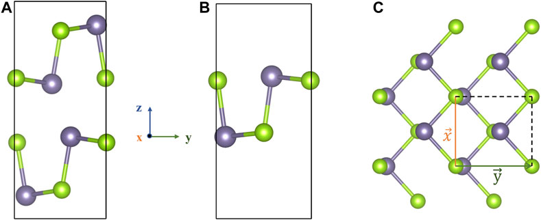
FIGURE 1. The atomic structures of (A) bulk and (B) monolayer GeSe. (C) The top view of monolayer GeSe. The dark and green spheres represent Ge and Se atoms, respectively.
We first optimize the lattice parameters of the bulk structure to compare to experimental lattices, shown in Table1. As we can see, there is a large lattice difference of the b axis (b axis is the armchair direction) under various pseudopotentials and methods for bulk structure. DFT-D2 (vdW-D2) and DFT-D3 (vdW-D3) method of Grimme is applied as vdW correction (Grimme, 2006). The optimized structure with the vdW-D2 method is in good agreement with experimental results compared to others. As to LDA and GGA methods, the lattice parameters is underestimated by 4 and 2.5% of the b axis, respectively. Based on these calculated structures, we investigate the Raman frequencies, and we find vdW-D2 gives a credible result in comparison to other methods, consistent with previous work (Park et al., 2019). Hence the interlayer interactions will be considered in the following calculations of bulk and multilayer structures. We should note that the Ag2 mode obtained in theoretical calculations was not observed in experiments on GeSe (Wang et al., 2017) but appears in the similar system SnSe (Yang et al., 2018), which is due to the Raman tensor of Ag2 mode is too small for its Raman peak to be observed in GeSe.
TABLE 1. The calculated structure lattice parameters (in the unit of Å) of bulk GeSe with various methods.
According to the above comparison and analysis, we use the vdW-D2 method to relax our structure and calculate the optical phonon frequencies. To understand the Raman frequencies of bulk GeSe, we analyze the crystal structure by combining the irreducible representations of Γ points. The primitive unit cell of bulk GeSe include eight atoms, resulting in 24 vibrational modes as following:
and
which are three acoustical (B1u, B2u, B3u), seven infrared active modes (3B1u, B2u, 3B3u), two silent modes (2Au), as well as twelve Raman modes (4Ag, 2B1g, 4B2g, 2B3g). Four active Raman modes for bulk GeSe as 3Ag at 68.21 cm−1, 179.05 cm−1, and 189.6 cm−1and B3g at 153.02 cm−1 are listed in Table 2, and we define 3Ag as Ag1, Ag2 and Ag3, respectively. To study the four active phonon vibration modes, we projected the eigenvectors of the dynamical matrix on Ge and Se atoms. Figure 2 gives the outline of the four vibration active modes of bulk GeSe. We find that Ag1, Ag2 and Ag3 couple the in-plane and out-of-plane vibrations with various contribution. Ag1 and Ag2 modes are mainly dominated by out-of-plane motion, in which Ge and Se atoms (Ge1 and Se2) move to the opposite direction of Ag1 mode whereas in Ag2 mode they move to the same direction. Ag3 mode is most contributed by armchair direction, and only the Ge atom has a small out-of-plane contribution. For Ag3 mode, it forms by an in-plane vibration along the armchair direction, indicating an intrinsic ferroelectric vibration mode in one layer of bulk GeSe, which agrees with previous experiment work (Zhao et al., 2018).
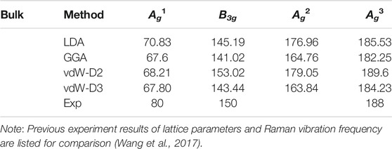
TABLE 2. The Raman vibration frequency (in the unit of cm−1) of bulk GeSe with different methods.

FIGURE 2. The activate Raman vibration mode of bulk GeSe. The out-of-plane along z direction.
Monolayer GeSe has been predicted a member of ferrovalley materials with plenty of fantastic physical properties (Morales-Ferreiro et al., 2017; Shen et al., 2018; Liu et al., 2021). Thus, it is necessary to investigate the Raman spectrum dependence of few-layer. For monolayer GeSe, the four active Raman peaks of Ag1, B3g, Ag2, and Ag3 modes are located at 81.84 cm−1, 97.54 cm−1, 141.94 cm−1, and 183.14 cm−1 illustrated in Table 3. Even though, both of paraelectric and ferroelectric phases exist in monolayer GeSe, we investigate the FE phase in the current work due to its lower energy state and stable structure. With the increase of thickness from monolayer to trilayer, the Raman shift changes a lot. Indeed, Ag1 mode generates a redshift from 81.84 cm−1 in the monolayer to 69.26 cm−1 in the bilayer. As to the remanent modes, they all increase. However, few shifts are induced between bilayer and trilayer. Our calculation suggests that GeSe has a large Raman shift with increasing layer thickness compared to other 2D materials (Lee et al., 2010; Tan et al., 2012; Yagmurcukardes et al., 2018; Kong et al., 2021). It provides a valuable approach for distinguishing the structure between monolayer and few-layer GeSe. The reason for such a large discrepancy of Raman peaks between monolayer and multilayer is attributed to the interlayer vdW interactions in multilayer GeSe, giving rise to structures difference. As a result, the lattice parameters that is listed in Table 3 along the armchair direction of monolayer GeSe are largely smaller than that of bilayer and trilayer.
TABLE 3. The lattice constant and activate Raman frequency (in the unit of Å and cm−1) for monolayer, bilayer and trilayer GeSe.
The Influence of Strain on Raman Peaks
Considering materials always are in strain in heterostructure or different temperatures, the influence of strain on Raman active modes is further explored in bulk and few-layer GeSe by changing the lattice parameter on both armchair and zigzag direction, as depicted in Figure 3. In monolayer GeSe, with the varying strain from −2 to 2%, the vibration mode of Ag1 linearly decreases in frequency. On the contrary, Ag2 and Ag3 modes exhibit a clear increase with strain. And for B3g mode, an inconspicuous change has been observed. Raman peaks between bilayer and trilayer GeSe possess the same trend in tensile and compressive strains. It should be mentioned that Raman frequency of Ag1 mode is most steady and rarely changed compared with the other three modes. Whereas, B3g and Ag3 modes increase by compressive strain and decrease along with tensile strain in Figures 3B,C. Moreover, as the strain increases, the gap of Raman shift among Ag2 and Ag3 modes is shrunk. Our results suggest that the stain has a great effect on the Raman shift, which can be detected in the experiment, demonstrating the stress dependence of Raman spectra can also be used for the determination of crystal direction.
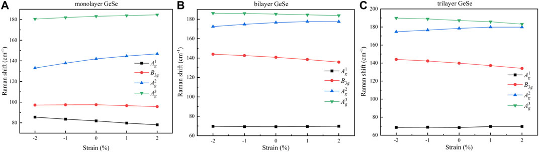
FIGURE 3. The influence of the Raman frequency on strain from −2 to 2% for (A) monolayer, (B) bilayer and (C) trilayer GeSe.
Interlayer Shift-Induced Raman Shift
Besides FE phase, AFE phase GeSe is also considered to be the lowest energy phase in an even number of layers. However, in some ways, the FE phase is more desired by researchers to utilize in multifunctional devices. To date, only the theoretical studies of AFE/FE transition for GeSe multilayers have been reported rather than any experimental works (Xu et al., 2021). Therefore, it is remarkable things to investigate the interlayer shift-induced AFE/FE transition and relevant Raman shift in few-layer GeSe. To realize the phase transition, we consider the AFE phase as a start structure. The structure evolution of the AFE/FE transition is illustrated in Figure 4. In bilayer GeSe, the bottom layer GeSe is fixed and the top layer artificially shifted along-y-direction in Figure 4A. When the top layer was shifted about 0.4b (b is the lattice parameter of y-direction), the system translates to an FE state. The same phenomenon appears in trilayer GeSe, in which we move interlayer between the top and bottom layer that is in fixation, showing in Figure 4B. Each shifted structure has been fully relaxed so that the Raman spectrum is obtained with a stable structure. Figures 5A,B represents the Raman shift in the intermediate phase. Ag1 mode of FE phase increases by of about 10 cm−1 compared with AFE phase in both bilayer and trilayer GeSe. Meanwhile. B3g, Ag2, and Ag3 mode show a redshift, in which the same variation rule in Ag2 mode is observed in both of bilayer and trilayer GeSe. In bilayer GeSe, Ag3 mode decreases with a nearly linear slope, yet it firstly increases and then diminishes with the interlayer shift of the trilayer. These large discrepancies in the Raman shift could be taken as an explicit evidence to identify the induced AFE/FE transition in the experiment.
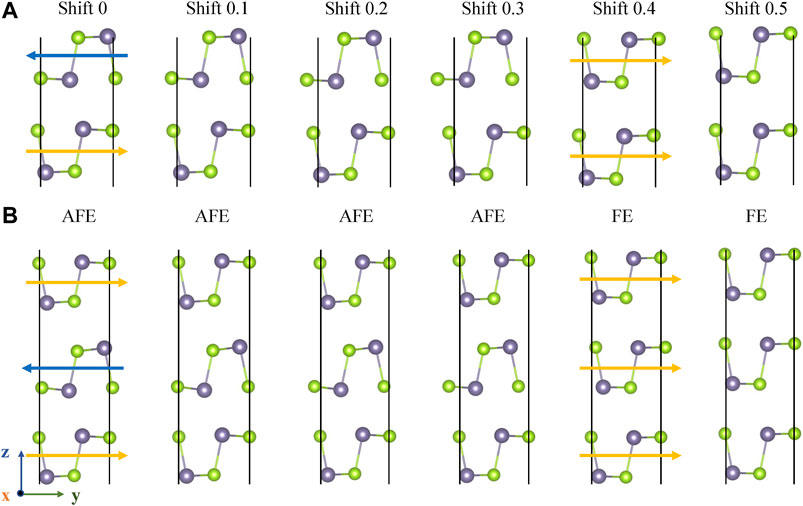
FIGURE 4. The evolution structures of AFE/FE transition by layer shift for (A) bilayer GeSe and (B) trilayer GeSe. The arrows represent the ferroelectric polarization direction. The shift n (n = 0, 0.1, 0.2, 0.3, 0.4, 0.5) represent the multiples of lattice parameter. The direction of arrows means the polarization direction of one-layer GeSe.

FIGURE 5. The activate Raman frequency related to the evolution structures for (A) bilayer and (B) trilayer GeSe in Figure 4.
Conclusion
To summarize, the Raman frequency of few-layer and bulk GeSe is systematically investigated using first-principles calculations. A large difference of Raman peaks between the monolayer and the multilayer, demonstrating the significant effect of vdW interlayer interaction. We then find the strain influence on these systems, in which Ag2 linearly increases and B3g mode linearly diminishes from −2 to 2%. More important, the interlayer shift could also induce a phase transition from AFE to FE. As a result, the Raman frequency discrepancy of four vibration modes is natural. We truly expect our calculations can pave a way to verify the number of layers, strain influence, and polarity in few-layer GeSe.
Data Availability Statement
The raw data supporting the conclusion of this article will be made available by the authors, without undue reservation.
Author Contributions
C-GD and NZ conceived the idea and supervised the work. Y-FZ carried out theory calculations. All authors analyzed the results and contributed to writing the manuscript.
Funding
This paper was supported by the National Key Research and Development Program of China (2017YFA0303403), Shanghai Science and Technology Innovation Action Plan (No. 19JC1416700), Natural Science Foundation of Shanghai (Grant No. 20ZR1418300) and the National Natural Science Foundation of China (No. 11774092, 61790583, 61874043, and 12074119). Computations were performed at the East China Normal University Multifunctional Platform for Innovation.
Conflict of Interest
The authors declare that the research was conducted in the absence of any commercial or financial relationships that could be construed as a potential conflict of interest.
Publisher’s Note
All claims expressed in this article are solely those of the authors and do not necessarily represent those of their affiliated organizations, or those of the publisher, the editors and the reviewers. Any product that may be evaluated in this article, or claim that may be made by its manufacturer, is not guaranteed or endorsed by the publisher.
Supplementary Material
The Supplementary Material for this article can be found online at: https://www.frontiersin.org/articles/10.3389/fmats.2021.736057/full#supplementary-material
References
Barone, V., Casarin, M., Forrer, D., Pavone, M., Sambi, M., and Vittadini, A. (2009). Role and Effective Treatment of Dispersive Forces in Materials: Polyethylene and Graphite Crystals as Test Cases. J. Comput. Chem. 30 (6), 934–939. doi:10.1002/jcc.21112
Baroni, S., de Gironcoli, S., Dal Corso, A., and Giannozzi, P. (2001). Phonons and Related crystal Properties from Density-Functional Perturbation Theory. Rev. Mod. Phys. 73 (2), 515–562. doi:10.1103/RevModPhys.73.515
Ceriotti, M., Pietrucci, F., and Bernasconi, M. (2006). Ab Initiostudy of the Vibrational Properties of crystallineTeO2: Theα,β, Andγphases. Phys. Rev. B 73 (10), 104304. doi:10.1103/PhysRevB.73.104304
Chang, K., Liu, J., Lin, H., Wang, N., Zhao, K., Zhang, A., et al. (2016). Discovery of Robust In-Plane Ferroelectricity in Atomic-Thick SnTe. Science 353 (6296), 274–278. doi:10.1126/science.aad8609
Chang, K., Miller, B. J., Yang, H., Lin, H., Parkin, S. S. P., Barraza-Lopez, S., et al. (2019). Standing Waves Induced by Valley-Mismatched Domains in Ferroelectric SnTe Monolayers. Phys. Rev. Lett. 122 (20), 206402. doi:10.1103/PhysRevLett.122.206402
Deng, Z., Li, Z., Wang, W., and She, J. (2019). Vibrational Properties and Raman Spectra of Pristine and Fluorinated Blue Phosphorene. Phys. Chem. Chem. Phys. 21 (3), 1059–1066. doi:10.1039/c8cp05699d
Ding, J., Shao, D.-F., Li, M., Wen, L.-W., and Tsymbal, E. Y. (2021). Two-Dimensional Antiferroelectric Tunnel Junction. Phys. Rev. Lett. 126 (5), 057601. doi:10.1103/PhysRevLett.126.057601
Ding, W., Zhu, J., Wang, Z., Gao, Y., Xiao, D., Gu, Y., et al. (2017). Prediction of intrinsic two-dimensional ferroelectrics in In2Se3 and other III2-VI3 van der Waals materials. Nat. Commun. 8, 14956. doi:10.1038/ncomms14956
Duan, C.-G., Sabirianov, R. F., Mei, W.-N., Jaswal, S. S., and Tsymbal, E. Y. (2006). Interface Effect on Ferroelectricity at the Nanoscale. Nano Lett. 6 (3), 483–487. doi:10.1021/nl052452l
Fei, R., Kang, W., and Yang, L. (2016). Ferroelectricity and Phase Transitions in Monolayer Group-IV Monochalcogenides. Phys. Rev. Lett. 117 (9), 097601. doi:10.1103/PhysRevLett.117.097601
Feng, Y., Zhou, J., Du, Y., Miao, F., Duan, C.-G., Wang, B., et al. (2015). Raman Spectra of Few-Layer Phosphorene Studied from First-Principles Calculations. J. Phys. Condens. Matter 27 (18), 185302. doi:10.1088/0953-8984/27/18/185302
Ferrari, A. C., Meyer, J. C., Scardaci, V., Casiraghi, C., Lazzeri, M., Mauri, F., et al. (2006). Raman Spectrum of Graphene and Graphene Layers. Phys. Rev. Lett. 97 (18), 187401. doi:10.1103/PhysRevLett.97.187401
Franzman, M. A., Schlenker, C. W., Thompson, M. E., and Brutchey, R. L. (2010). Solution-Phase Synthesis of SnSe Nanocrystals for Use in Solar Cells. J. Am. Chem. Soc. 132 (12), 4060–4061. doi:10.1021/ja100249m
Garcia, V., Fusil, S., Bouzehouane, K., Enouz-Vedrenne, S., Mathur, N. D., Barthélémy, A., et al. (2009). Giant Tunnel Electroresistance for Non-destructive Readout of Ferroelectric States. Nature 460 (7251), 81–84. doi:10.1038/nature08128
Giannozzi, P., Baroni, S., Bonini, N., Calandra, M., Car, R., Cavazzoni, C., et al. (2009). QUANTUM ESPRESSO: a Modular and Open-Source Software Project for Quantum Simulations of Materials. J. Phys. Condens. Matter 21 (39), 395502. doi:10.1088/0953-8984/21/39/395502
Gonze, X., Stumpf, R., and Scheffler, M. (1991). Analysis of Separable Potentials. Phys. Rev. B 44 (16), 8503–8513. doi:10.1103/PhysRevB.44.8503
Grimme, S. (2006). Semiempirical GGA-type Density Functional Constructed with a Long-Range Dispersion Correction. J. Comput. Chem. 27 (15), 1787–1799. doi:10.1002/jcc.20495
Guan, Z., Hu, H., Shen, X., Xiang, P., Zhong, N., Chu, J., et al. (2020). Recent Progress in Two‐Dimensional Ferroelectric Materials. Adv. Electron. Mater. 6 (1), 1900818. doi:10.1002/aelm.201900818
Higashitarumizu, N., Kawamoto, H., Lee, C.-J., Lin, B.-H., Chu, F.-H., Yonemori, I., et al. (2020). Purely In-Plane Ferroelectricity in Monolayer SnS at Room Temperature. Nat. Commun. 11 (1), 2428. doi:10.1038/s41467-020-16291-9
Hohenberg, P., and Kohn, W. (1964). Inhomogeneous Electron Gas. Phys. Rev. 136 (3B), B864–B871. doi:10.1103/PhysRev.136.B864
Huang, C., Du, Y., Wu, H., Xiang, H., Deng, K., and Kan, E. (2018a). Prediction of Intrinsic Ferromagnetic Ferroelectricity in a Transition-Metal Halide Monolayer. Phys. Rev. Lett. 120 (14), 147601. doi:10.1103/PhysRevLett.120.147601
Huang, W., Fang, Y.-W., Yin, Y., Tian, B., Zhao, W., Hou, C., et al. (2018b). Solid-State Synapse Based on Magnetoelectrically Coupled Memristor. ACS Appl. Mater. Inter. 10 (6), 5649–5656. doi:10.1021/acsami.7b18206
Junquera, J., and Ghosez, P. (2003). Critical Thickness for Ferroelectricity in Perovskite Ultrathin Films. Nature 422 (6931), 506–509. doi:10.1038/nature01501
Kohn, W., and Sham, L. J. (1965). Self-Consistent Equations Including Exchange and Correlation Effects. Phys. Rev. 140 (4A), A1133–A1138. doi:10.1103/PhysRev.140.A1133
Kong, X., Berlijn, T., and Liang, L. (2021). Thickness and Spin Dependence of Raman Modes in Magnetic Layered Fe 3 GeTe 2. Adv. Electron. Mater. 7, 2001159. doi:10.1002/aelm.202001159
Lee, C., Yan, H., Brus, L. E., Heinz, T. F., Hone, J., and Ryu, S. (2010). Anomalous Lattice Vibrations of Single- and Few-Layer MoS2. ACS Nano 4 (5), 2695–2700. doi:10.1021/nn1003937
Lin, L.-F., Zhang, Y., Moreo, A., Dagotto, E., and Dong, S. (2019). Frustrated Dipole Order Induces Noncollinear Proper Ferrielectricity in Two Dimensions. Phys. Rev. Lett. 123 (6), 067601. doi:10.1103/PhysRevLett.123.067601
Liu, F., You, L., Seyler, K. L., Li, X., Yu, P., Lin, J., et al. (2016). Room-temperature Ferroelectricity in CuInP2S6 Ultrathin Flakes. Nat. Commun. 7, 12357. doi:10.1038/ncomms12357
Liu, S.-C., Dai, C.-M., Min, Y., Hou, Y., Proppe, A. H., Zhou, Y., et al. (2021). An Antibonding Valence Band Maximum Enables Defect-Tolerant and Stable GeSe Photovoltaics. Nat. Commun. 12 (1), 670. doi:10.1038/s41467-021-20955-5
Mathews, S., Ramesh, R., Venkatesan, T., and Benedetto, J. (1997). Ferroelectric Field Effect Transistor Based on Epitaxial Perovskite Heterostructures. Science 276 (5310), 238–240. doi:10.1126/science.276.5310.238
Morales-Ferreiro, J. O., Diaz-Droguett, D. E., Celentano, D., and Luo, T. (2017). First-Principles Calculations of Thermoelectric Properties of IV-VI Chalcogenides 2D Materials. Front. Mech. Eng. 3 (15), 15. doi:10.3389/fmech.2017.00015
Park, M., Choi, J. S., Yang, L., and Lee, H. (2019). Raman Spectra Shift of Few-Layer IV-VI 2D Materials. Sci. Rep. 9, 19826. doi:10.1038/s41598-019-55577-x
Perdew, J. P., Burke, K., and Ernzerhof, M. (1996). Generalized Gradient Approximation Made Simple. Phys. Rev. Lett. 77 (18), 3865–3868. doi:10.1103/PhysRevLett.77.3865
Perdew, J. P., and Zunger, A. (1981). Self-interaction Correction to Density-Functional Approximations for many-electron Systems. Phys. Rev. B 23 (10), 5048–5079. doi:10.1103/PhysRevB.23.5048
Rodin, A. S., Gomes, L. C., Carvalho, A., and Castro Neto, A. H. (2016). Valley Physics in Tin (II) Sulfide. Phys. Rev. B 93 (4), 045431. doi:10.1103/PhysRevB.93.045431
Saboori, S., Deng, Z., Li, Z., Wang, W., and She, J. (2019). β-As Monolayer: Vibrational Properties and Raman Spectra. ACS Omega 4 (6), 10171–10175. doi:10.1021/acsomega.9b00712
Scott, J. F., and Paz de Araujo, C. A. (1989). Ferroelectric Memories. Science 246 (4936), 1400–1405. doi:10.1126/science.246.4936.1400
Shen, X.-W., Fang, Y.-W., Tian, B.-B., and Duan, C.-G. (2019). Two-Dimensional Ferroelectric Tunnel Junction: The Case of Monolayer In:SnSe/SnSe/Sb:SnSe Homostructure. ACS Appl. Electron. Mater. 1 (7), 1133–1140. doi:10.1021/acsaelm.9b00146
Shen, X.-W., Tong, W.-Y., Gong, S.-J., and Duan, C.-G. (2018). Electrically Tunable Polarizer Based on 2D Orthorhombic Ferrovalley Materials. 2d Mater. 5 (1), 011001. doi:10.1088/2053-1583/aa8d3b
Shi, G., and Kioupakis, E. (2015). Anisotropic Spin Transport and Strong Visible-Light Absorbance in Few-Layer SnSe and GeSe. Nano Lett. 15 (10), 6926–6931. doi:10.1021/acs.nanolett.5b02861
Song, S., Zhang, Y., Guan, J., and Dong, S. (2021). Noncollinear Ferrielectricity and Morphotropic Phase Boundary in Monolayer GeS. Phys. Rev. B 103 (14), L140104. doi:10.1103/PhysRevB.103.L140104
Tan, P. H., Han, W. P., Zhao, W. J., Wu, Z. H., Chang, K., Wang, H., et al. (2012). The Shear Mode of Multilayer Graphene. Nat. Mater. 11 (4), 294–300. doi:10.1038/Nmat3245
Tian, B., Liu, L., Yan, M., Wang, J., Zhao, Q., Zhong, N., et al. (2019). A Robust Artificial Synapse Based on Organic Ferroelectric Polymer. Adv. Electron. Mater. 5 (1), 1800600. doi:10.1002/aelm.201800600
Umari, P., Pasquarello, A., and Dal Corso, A. (2001). Raman Scattering Intensities in α-quartz: A First-Principles Investigation. Phys. Rev. B 63 (9), 094305. doi:10.1103/PhysRevB.63.094305
Velev, J. P., Duan, C.-G., Belashchenko, K. D., Jaswal, S. S., and Tsymbal, E. Y. (2007). Effect of Ferroelectricity on Electron Transport inPt/BaTiO3/PtTunnel Junctions. Phys. Rev. Lett. 98 (13), 137201. doi:10.1103/PhysRevLett.98.137201
Wang, H., and Qian, X. (2017). Two-dimensional Multiferroics in Monolayer Group IV Monochalcogenides. 2d Mater. 4 (1), 015042. doi:10.1088/2053-1583/4/1/015042
Wang, X., Li, Y., Huang, L., Jiang, X.-W., Jiang, L., Dong, H., et al. (2017). Short-Wave Near-Infrared Linear Dichroism of Two-Dimensional Germanium Selenide. J. Am. Chem. Soc. 139 (42), 14976–14982. doi:10.1021/jacs.7b06314
Wang, Y., Niranjan, M. K., Janicka, K., Velev, J. P., Zhuravlev, M. Y., Jaswal, S. S., et al. (2010). Ferroelectric Dead Layer Driven by a Polar Interface. Phys. Rev. B 82 (9), 094114. doi:10.1103/PhysRevB.82.094114
Wu, M., and Jena, P. (2018). The rise of two‐dimensional van der Waals ferroelectrics. Wires Comput. Mol. Sci. 8 (5), e1365. doi:10.1002/wcms.1365
Xu, B., Deng, J., Ding, X., Sun, J., and Liu, J. Z. (2021). Interlayer Sliding Induced Intralayer Ferroelectric-Antiferroelectric Transition in Bilayer Group-IV Monochalcogenides. arXiv preprint arXiv:2103.12518.
Yagmurcukardes, M., Peeters, F. M., and Sahin, H. (2018). Electronic and Vibrational Properties of PbI2 : From Bulk to Monolayer. Phys. Rev. B 98 (8), 085431. doi:10.1103/PhysRevB.98.085431
Yagmurcukardes, M., Senger, R. T., Peeters, F. M., and Sahin, H. (2016). Mechanical Properties of Monolayer GaS and GaSe Crystals. Phys. Rev. B 94 (24), 245407. doi:10.1103/PhysRevB.94.245407
Yang, S., Liu, Y., Wu, M., Zhao, L.-D., Lin, Z., Cheng, H.-c., et al. (2018). Highly-anisotropic Optical and Electrical Properties in Layered SnSe. Nano Res. 11 (1), 554–564. doi:10.1007/s12274-017-1712-2
You, L., Zhang, Y., Zhou, S., Chaturvedi, A., Morris, S. A., Liu, F., et al. (2019). Origin of giant negative piezoelectricity in a layered van der Waals ferroelectric. Sci. Adv. 5 (4), eaav3780. doi:10.1126/sciadv.aav3780
Yuan, S., Luo, X., Chan, H. L., Xiao, C., Dai, Y., Xie, M., et al. (2019). Room-temperature Ferroelectricity in MoTe2 Down to the Atomic Monolayer Limit. Nat. Commun. 10, 1775. doi:10.1038/s41467-019-09669-x
Zhang, X., Qiao, X.-F., Shi, W., Wu, J.-B., Jiang, D.-S., and Tan, P.-H. (2015). Phonon and Raman Scattering of Two-Dimensional Transition Metal Dichalcogenides from Monolayer, Multilayer to Bulk Material. Chem. Soc. Rev. 44 (9), 2757–2785. doi:10.1039/c4cs00282b
Zhao, H., Mao, Y., Mao, X., Shi, X., Xu, C., Wang, C., et al. (2018). Band Structure and Photoelectric Characterization of GeSe Monolayers. Adv. Funct. Mater. 28 (6), 1704855. doi:10.1002/adfm.201704855
Keywords: GESE, Raman spectra, first-principales calculation, ferroelectric, antiferroelectric, ferrovalley
Citation: Zhao Y-F, Guan Z, Zhong N, Yue F-Y, Xiang P-H and Duan C-G (2021) Raman Spectra of Bulk and Few-Layer GeSe From First-Principles Calculations. Front. Mater. 8:736057. doi: 10.3389/fmats.2021.736057
Received: 04 July 2021; Accepted: 25 August 2021;
Published: 10 September 2021.
Edited by:
Weiliang Wang, Sun Yat-sen University, ChinaReviewed by:
Zhongming Wei, Institute of Semiconductors (CAS), ChinaZexiang Deng, The University of Hong Kong, Hong Kong, SAR China
Haiming Huang, Guangzhou University, China
Mehmet Yagmurcukardes, University of Antwerp, Belgium
Copyright © 2021 Zhao, Guan, Zhong, Yue, Xiang and Duan. This is an open-access article distributed under the terms of the Creative Commons Attribution License (CC BY). The use, distribution or reproduction in other forums is permitted, provided the original author(s) and the copyright owner(s) are credited and that the original publication in this journal is cited, in accordance with accepted academic practice. No use, distribution or reproduction is permitted which does not comply with these terms.
*Correspondence: Chun-Gang Duan, Y2dkdWFuQGNscG0uZWNudS5lZHUuY24=