 Shiyu Deng1
 Kun Chen
 Huanjun Chen
95% of researchers rate our articles as excellent or good
Learn more about the work of our research integrity team to safeguard the quality of each article we publish.
Find out more
ORIGINAL RESEARCH article
Front. Mater. , 17 August 2021
Sec. Thin Solid Films
Volume 8 - 2021 | https://doi.org/10.3389/fmats.2021.735344
This article is part of the Research Topic Electronic Properties, Vibrational Properties and Optical Properties of Van der Waals 2D Crystals View all 8 articles
Ultrathin hexagonal boron nitride (h-BN) has recently attracted a lot of attention due to its excellent properties. With the rapid development of chemical vapor deposition (CVD) technology to synthesize wafer-scale single-crystal h-BN, the properties of h-BN have been widely investigated with a variety of material characterization techniques. However, the electronic properties of monolayer h-BN have rarely been quantitatively determined due to its atomically thin thickness and high sensitivity to the surrounding environment. In this work, by the combined use of AFM (atomic force microscope) PeakForce Tunneling (PF-TUNA) mode and Kevin probe force microscopy (KPFM) model, both the electrical resistivity (529 MΩ cm) and the inherent Fermi level (∼4.95 eV) of the as-grown monolayer h-BN flakes on the copper substrate have been quantitatively analyzed. Moreover, direct visualization of the high-temperature oxidation-resistance effect of h-BN nanoflakes has been presented. Our work demonstrates a direct estimation of the electronic properties for 2D materials on the initial growth substrate without transfer, avoiding any unwanted contaminations introduced during the transfer process. The quantitative analysis by state-of-the-art atomic force microscope techniques implies that monolayer h-BN can be employed as an atomically thin and high-quality insulator for 2D electronics, as well as a high-temperature antioxidation layer for electronic device applications.
Ultrathin hexagonal boron nitride (h-BN) has recently attracted more and more attention because of its similarity to graphene in structure, as well as its demonstrated excellent properties (Dean et al., 2010; Liu et al., 2013a; Wang et al., 2019; Chen et al., 2020). Within each layer of h-BN, sp-bonded alternating boron and nitrogen atoms are arranged in a honeycomb lattice with a lattice constant of 0.252 nm (Dean et al., 2010). The h-BN is a promising deep ultraviolet emitter with intense 215 nm luminescence at room temperature due to its direct bandgap of 5.97 eV (Kubota et al., 2007). Besides, h-BN film has been integrated as a dielectric layer in graphene devices or as the electron tunneling barriers with a dielectric constant of four to six and a breakdown voltage of 8–10 MV/cm (Lee et al., 2011; Kim et al., 2012a; Britnell et al., 2012; Hattori et al., 2016). More importantly, h-BN can be used as a superior substrate for electronic devices of 2D materials due to its atomically smooth surface which is relatively free of dangling bonds and charge traps (Lee et al., 2012; Lee et al., 2015). Like graphene, high-quality monolayer and few-layer h-BN flakes can be exfoliated from bulk BN crystals by either mechanical cleavage (Pacilé et al., 2008) or a chemical-solution-derived method (Coleman et al., 2011; McManus et al., 2017). On the other hand, chemical vapor deposition (CVD) offers significant advantages for obtaining large area h-BN films by using various chemical precursors such as borazine (B3N3H6) (Shi et al., 2010) or ammonia borane (NH3-BH3) (Fazen et al., 1995; Kim et al., 2012b; Wang et al., 2019; Chen et al., 2020). The growth substrate plays a more important role in the synthesis of h-BN. For instance, epitaxial growth of single-crystal monolayer h-BN as large as 100 cm2 has been demonstrated on a low-symmetry Cu (110) vicinal surface (Wang et al., 2019). Wafer-scale single-crystal monolayer h-BN has also been obtained on Cu (111) surface, due to the lateral docking of h-BN to Cu (111) steps (Chen et al., 2020). So far, the electronic properties of multilayer h-BN have been widely reported. For example, the electrical resistivity of the hybrid atomic monolayer consisting of h-BN and graphene (h-BNC) can be tuned from the insulator to 10−3 Ω cm (Ci et al., 2010). The h-BN stripes of the in-plane graphene/h-BN heterostructures showed ∼2 pA current under the voltage bias of tens of millivolts (Liu et al., 2013b). The threshold resistive switching of multilayer h-BN/Cu stacks with a current compliance of less than 100 nA has been studied by conductive AFM (C-AFM, contact mode) (Ranjan et al., 2018). The leakage current for graphite/h-BN sandwich devices with 2 and 4 L h-BN has also been measured by C-AFM, corresponding to a resistance in the order of 10 MΩ–1 GΩ (Britnell et al., 2012). A broad variation in the resistance values of monolayer h-BN has been observed (Stehle et al., 2017). C-AFM has also been used to obtain the barrier height for tunneling (3.07 eV) of h-BN based on the Fowler-Nordheim tunneling (FNT) model (Lee et al., 2011). A fluctuation up to three orders of magnitude of the tunneling current across the h-BN stack from one substrate (Pt) grain to another has been reported (Hui et al., 2017). Despite these rapid developments of h-BN, the electronic properties of monolayer h-BN have been rarely quantitatively estimated due to its atomically thin thickness and high sensitivity to the surrounding environment (Steinborn et al., 2013; Qian et al., 2016; Jiang et al., 2017). In this work, monolayer h-BN nanoflakes with regular shapes have been synthesized on the copper foil and the electronic properties including the electrical resistivity (529 MΩ cm) and the inherent Fermi level (∼4.95 eV) of the CVD monolayer h-BN on the initial growth substrate have been quantitatively analyzed by the combined use of AFM PeakForce Tunneling (PF-TUNA) mode and Kevin probe force microscopy (KPFM) model, demonstrating that monolayer h-BN can be used as an atomically thin and high-quality insulator as well as an antioxidation layer.
The monolayer h-BN nanoflakes were grown on the inner side of the Cu-foil enclosure by customized low-pressure chemical vapor deposition (LPCVD) (Wan et al., 2021) with the precursor of solid NH3-BH3 since the growth of LPCVD is preferentially surface reaction limited and less affected by the geometry of the substrate or gas flow effect (Bhaviripudi et al., 2010). The synthesis of monolayer h-BN flakes was carried out in our CVD system (see Supplementary Figure S1A) which contains a split tube furnace with a fused quartz tube (OD: 50 mm) as shown in Figure 1A. A copper foil with 25 μm thickness was used as the growth substrate. Before growth, the copper foil was washed thoroughly by diluted nitric acid and deionized (DI) water. To obtain monolayer h-BN nanoflakes, copper-foil enclosure as depicted in Supplementary Figure S1B, formed by bending the flat Cu foil and then crimping the three remaining sides (Li et al., 2011), was adopted to lower the density of NH3-BH3. The h-BN film could grow on both the inside and the outside of the Cu-foil enclosure. The thickness of the resulting h-BN film on the outside could be in the range of 5–30 nm (see Supplementary Figure S2 and Supplementary Section S1), depending on the growth time as well as the amount of the precursors. On the other hand, monolayer h-BN flakes have been observed on the inside of the Cu-foil enclosure with a low density of nuclei as shown in Figure 1B, presumably due to the lower partial pressure of NH3-BH3 (Li et al., 2011). The Cu-foil enclosure was heated in an oven at 150–300°C in air for 1 h to visualize the h-BN nanoflakes. A typical growth process (see Supplementary Figure S1A) for monolayer h-BN is described as follows: 1) the copper-foil enclosure and ammonia borane were placed into the furnace and a glass tube, respectively. Then the pressure of the CVD system was evacuated down to ∼0.1 Pa; 2) the copper-foil enclosure was lately gradually heated to 1,050°C in 40 min and pure H2 (30 sccm) was introduced into the furnace at a pressure of ∼40 Pa by the mass flow controller (MFC); 3) after annealing at 1,050°C for 30°min, the copper-foil enclosure was stabilized at the desired growth temperature (∼1,030°C), and then NH3-BH3 was introduced into the system with the heating belt at a temperature ∼60–90°C; the growth time was tuned between 5 and 30 min; 4) after exposure to NH3-BH3, the copper-foil enclosure was quickly cooled down to room temperature under the atmosphere of H2 (2–10°sccm) and Ar (30–50°sccm) by directly opening the split tube furnace.
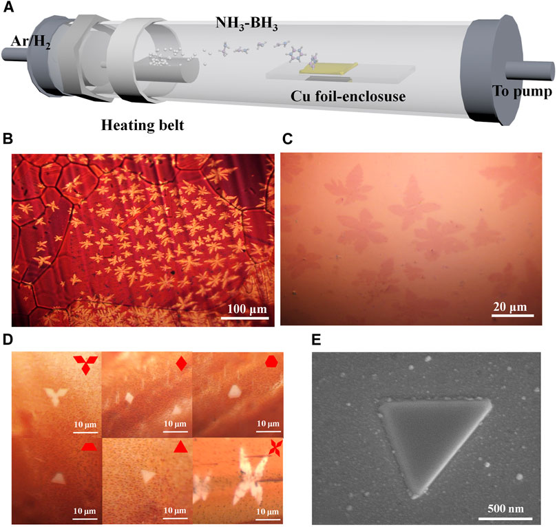
FIGURE 1. LPCVD synthesis of monolayer h-BN nanoflakes for the following AFM measurements. (A) Schematic of the LPCVD system for monolayer h-BN growth using Cu-foil enclosure. (B) Optical image of h-BN/Cu after oxidation. (C) Optical image of the wet-transferred monolayer h-BN on 300 nm thick SiO2/Si substrate. (D) Optical images of h-BN nanoflakes on the copper foil with various regular shapes. Insets: the schematic of h-BN nanoflakes. (E) SEM image of an h-BN monolayer on the copper substrate after oxidation. The brighter edge is due to the height difference between h-BN and copper oxide, which has been further confirmed by the following AFM measurements.
The SEM images were obtained by LEO 1450VP (operated at 5 kV). Raman spectroscopy measurement was performed using a Renishaw LabRAM Invia micro-Raman system with 532 nm laser excitation at room temperature and in the atmospheric environment. The laser spot size was around 1 μm by using a ×50 objective and the laser power was kept below 1 mW. Absorption spectroscopy was performed by using a UV-Vis spectrophotometer (UV-1900, Shimadzu). The XPS measurement was carried out on a Thermo VG ESCALAB 250 X-ray photoelectron spectrometer using a monochromated Al Kα (1,486.6 eV) X-ray source. The light spot of an X-ray was around 0.5 mm in diameter. The AFM measurement was carried out by using Dimension Icon system (Bruker) for the PF-TUNA mode and NTEGRA system (NT-MDT) for the KPFM mode. The standard commercial AFM tips with V-shaped cantilevers (NSC11/TiN) were used for the PF-TUNA mode. The tips were coated with a TiN layer of 20–30 nm thickness, whose curvature radius was ∼35 nm. KPFM measurement was performed using the conductive AFM tip (HA_NC/Pt, resonant frequency:140 kHz).
The as-grown h-BN films on the copper surface were transferred to target substrates by the wet-transfer method (see Supplementary Figure S5 and Supplementary Section S3). After that, the h-BN devices were fabricated by using a maskless UV lithography process (Direct Projection Lithography, TuoTuo Technology). Electrodes (∼5 nm thick Cr and ∼50 nm thick Au) were prepared by thermal evaporation under a vacuum of 1 × 10⁻³ Pa. The current−voltage (I−V) curves were measured using a Keithley 2636B source meter with a current resolution down to 0.1 fA controlled by a LabVIEW program.
Figure 1A shows the schematic of the LPCVD growth of monolayer h-BN on the inner side of the Cu-foil enclosure, during which the growth time plays an important role in the formation of the resulting h-BN nanoflakes. If the growth time was less than 15 min, the nucleation sites of h-BN with random shapes were distributed along the polished lines (Supplementary Figure S2A and Supplementary Section S2) on the copper surface, in good agreement with the previous result (Kim et al., 2012b). Supplementary Figures S2B–D display the scanning electron microscopy (SEM) images of h-BN nanoflakes with growth time ranging from 5 to 15 min. It can be clearly observed that both flake size and the density of h-BN nuclei/islands increased with prolonged growth time. As shown in Figure 1B and Supplementary Figure S4, if the growth time was further increased to 20–30°min, the h-BN nanoflakes can be observed across the entire surface on the inner side of the Cu-foil enclosure. Figure 1C shows the wet-transferred snowflake-shaped h-BN sheets on the 300 nm thick SiO2/Si substrate. Moreover, other regular shapes including the Mitsubishi-shaped, diamond-like, hexagonal, ladder-shaped, triangle, and butterfly-shaped h-BN nanoflakes can be observed as depicted in Figure 1D. Figure 1E presents the SEM image of the resulting triangle h-BN nanoflakes on the copper substrate after the oxidation.
Raman spectroscopy is a powerful tool to analyze the h-BN lattice vibration modes which are due to the stretching of the bonds between the nitrogen and boron atoms (Shi et al., 2010; Song et al., 2010). The Raman spectrum in Figure 2A shows one dominant peak at 1,368.7°cm−1, which can be assigned to the E2g vibration mode of h-BN, confirming the BN film with a hexagonal structure. Compared with the E2g mode of bulk BN film (∼1,370.9°cm−1), this peak was shifted down about 2.2°cm−1. In general, the Raman peak frequency would be shifted to higher and lower frequency under compressive and tensile stress, respectively (Song et al., 2010). Therefore, the redshift of the Raman peak could be due to an increase of stress in the h-BN films, which could be formed by the substrate interaction and the intrinsic surface wrinkles as shown in Supplementary Figure S2B. To investigate the optical properties, UV-visible absorption measurement has been performed and the results are shown in Figure 2B. According to the absorption equation (Shi et al., 2010; Song et al., 2010; Kim et al., 2012b),
where A is the optical absorption of the h-BN film and L is the film thickness, the absorption coefficient α at each photon energy E can be obtained. The optical band gap Eg (OBG) can be estimated by a straight-line fitting as shown in Figure 2B (the dark line) using the following equation (Kim et al., 2012b):
where C is a constant. When αE = 0, the corresponding E equals Eg and the optical band gap Eg was estimated to be around ∼5.74 eV, which is consistent with the previous literature (Kim et al., 2012b; Bhaviripudi et al., 2010; Song et al., 2010). X-ray photoelectron spectroscopy (XPS) has also been applied to characterize the elemental stoichiometry of the synthesized h-BN samples. Figure 2E shows the XPS spectra of transferred h-BN films on 300 nm thick SiO2/Si substrate. The binding energies for boron 1s and nitrogen 1s are shown in Figures 2C,D, respectively. The observed binding energies of B 1s and N 1s and from the XPS measurement were 190.68 and 398.24 eV, respectively, in good agreement with the literature values (Shi et al., 2010; Kim et al., 2012b; Song et al., 2010). Both the B 1s and the N 1s spectra indicate that the configuration for B and N atoms was the B-N bond, implying that the hexagonal phase exists in the BN films. The B/N stoichiometry from the XPS survey has been calculated to be ∼0.9. The excess N could be due to the exposure of the h-BN film to the atmosphere in between the film growth and the XPS measurement. Moreover, O 1s (532.92 eV) and C 1s (284.8 eV) peaks are observed in our samples as shown in Figure 2E, which could also result from the exposure of the h-BN film to air. Since the X-ray is expected to penetrate through the h-BN film down to several nanometers (Shi et al., 2010), a small Si 2p peak (101.96 eV) (inset in Figure 2E) could be from the underlying SiO2/Si substrate.
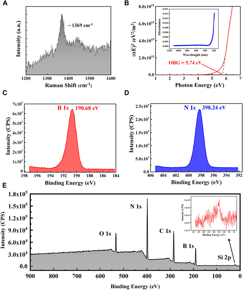
FIGURE 2. Characterizing of h-BN samples. (A) Raman spectrum of the h-BN sample transferred on a SiO2/Si substrate. (B) The optical band gap analysis and inset is UV-visible absorption spectrum. (C) B1s and (D) N1s XPS spectra of the h-BN sample, respectively. (E) XPS survey spectrum of the h-BN on SiO2/Si substrate. The inset displays the XPS spectrum of Si 2p.
To gain the insight of the resistivity (ρ) of monolayer h-BN, AFM PF-TUNA mode (Figures 3A,B) has been performed on monolayer h-BN grown on the copper surface. By using the PF-TUNA model, the force between the tip and sample could be precisely controlled, and the problem arising from using C-AFM to measure nanoelectrical properties could be solved. During the measurement, a constant force between tip and sample was maintained, and thus the topographic and current images could be simultaneously generated, enabling the direct correlation of local topography with the electrical properties. Figure 3C displays the 3D height image of h-BN on the copper surface, showing the polished lines and the groove between them. Since the thickness of monolayer h-BN is only ∼0.32 nm (Kim et al., 2012b), it is difficult to distinguish h-BN from the copper surface. The particles on the sample were believed to come from the quartz tube used in the LPCVD chamber, as reported by the literature (Zhang et al., 2012). In contrast to the AFM topological image, both the TUNA current image (Figure 3D) and the phase image (see Supplementary Figure S7 and Supplementary Section S4) clearly reveal that the h-BN nanoflakes occur along the polished lines, which is consistent with the SEM results as well as the previous literature (Kim et al., 2012b). Figure 3E shows a line profile of the TUNA current taken from the red line in Figure 3D, which is the average current over one full tapping cycle at a sample position, including the current measured when the tip is in contact with the sample surface as well as when it is off the sample surface (see Supplementary Figure S6) (Schillers et al., 2016; Slattery et al., 2018). The resistance Rh-BN of monolayer h-BN can be obtained by
where V = 10 V is the bias voltage applied between the conductive tip and sample, Rtip, RAir, and RCu are the resistance of AFM tip, the air resistance between tip and sample, and the resistance of copper substrate, respectively (Figure 3B). The obtained Rh-BN is ∼430 GΩ, exhibiting the insulating characteristics of h-BN. The histogram distribution of total TUNA resistance is shown in Figure 3F, clearly revealing two pronounced peaks at ∼ 40 and ∼480 GΩ for Cu and h-BN/Cu, respectively, given the resistance (R) of monolayer h-BN ∼ 440 GΩ, which is consistent with the value obtained from the line profile. For the h-BN/Cu sample under the conductive AFM tip, the tunneling behavior is more complicated but can be understood by the typical theoretical model of the tunneling current, which is given by (Bai, 2000; Britnell et al., 2012)
where DOSs(E) and DOSt(E) are the density of states of the sample and tip, respectively, T(E) is the transmission probability at the given energy and f(E) is the Fermi distribution function, and Aeff is the effective area through which the TUNA current can flow. In the C-AFM mode, Aeff can be estimated by
where Rtip is the radius of AFM tip, F is the contact force between sample and tip, and K is related to the elasticity moduli and the Poisson ratios of the tip and the samples (Frammelsberger et al., 2007). For a Pt-Ir coated tip with Rtip = 20 nm on insulating SiO2, the Aeff is in the range of 50–200 nm2 (Frammelsberger et al., 2007). However, for the PF-TUNA mode, the Z-piezo with the tip is modulated by a default amplitude of 150 nm at 1–2 kHz (Schillers et al., 2016; Slattery et al., 2018) and during the TUNA current measurement, the tip is tens of nm away from the sample surface for most of the time. Thus, the effective area Aeff as indicated in Figure 3B is estimated by the projected area of the tip on the sample surface, which is ∼3,800 nm2 for Rtip = 35 nm, in good agreement with the value reported by previous literature (Lee et al., 2011). The resistivity (ρ) of monolayer h-BN is estimated by
where t = 0.32 nm is the thickness of monolayer h-BN (Kim et al., 2012b). Thus, the estimated resistivity of monolayer h-BN is ∼529 MΩ cm, which is consistent with our analysis of the resistivity (∼501 MΩ cm) of 14 nm thick h-BN film (see Supplementary Figure S8 and Supplementary Section S5). It should be noted that the resistivity estimated by the direct current tunneling through graphite/h-BN/Au demonstrated an exponential dependence on the h-BN thickness as expected for the quantum tunneling theory (Bai, 2000; Britnell et al., 2012). However, the measured PF-TUNA current is the average current over one entire tapping cycle, including the current while the tip is approaching the surface as well as when it is off the surface. Thus, our estimated resistivity of monolayer h-BN is close to the intrinsic h-BN resistivity.
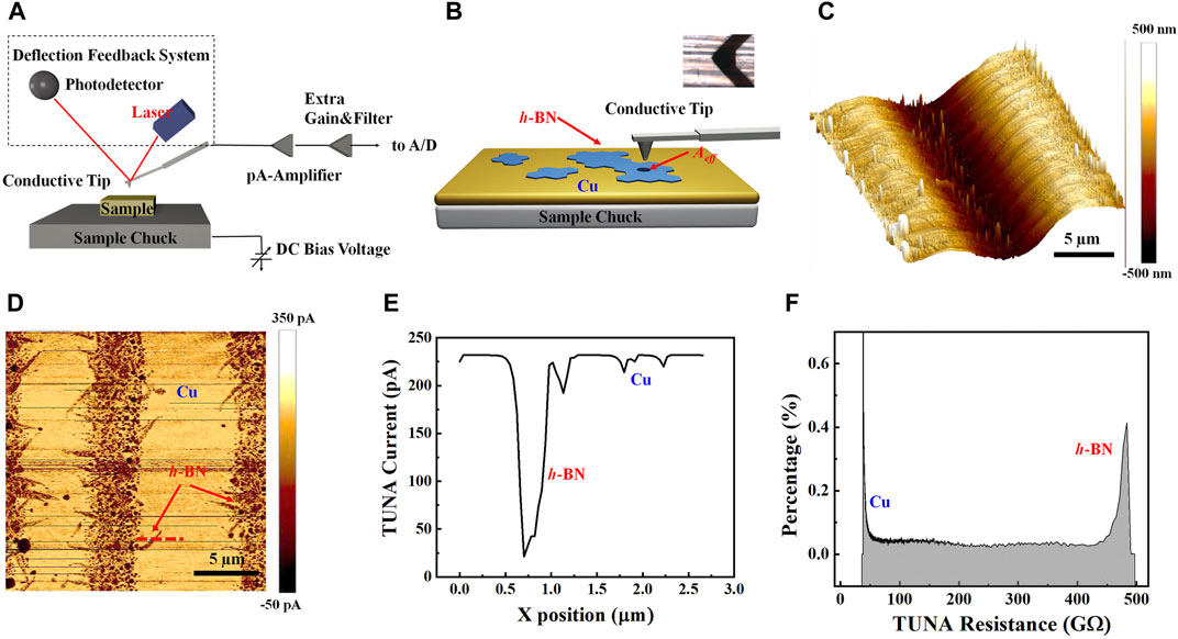
FIGURE 3. AFM PF-TUNA measurements of monolayers h-BN nanoflakes on Cu. (A) Schematic of the working principle of AFM PF-TUNA mode. (B) Diagram of the measurement setup of TUNA current between the conductive AFM tip (inset) and monolayer h-BN on copper substrate. (C) AFM height image of as-grown monolayer h-BN on copper. (D) PF-TUNA current mapping of h-BN monolayer on copper. (E) A line profile of the TUNA current taken from the red line in panel (D). (F) The histogram distribution of the TUNA resistance.
X-ray diffraction analysis has been carried out to identify the crystalline phases present in the Cu substrate. Since the copper oxidation is inevitable in air, the Cu foil was firstly annealed in an oven at 150–300°C for 1 h to ensure the visualization of the h-BN nanoflakes on the copper substrate, as well as to realize the full formation of CuO (111) on top of the Cu foil without the covering and protection of h-BN flakes (Duong et al., 2012). Figure 4A shows the XRD patterns obtained by a 2θ scan of the Cu substrate before (black line) and after (blue line) oxidation. Before the oxidation in air, the presence of only one sharp Cu (111) peak at ∼ 43.3° in the XRD pattern (black line in Figure 4A) confirmed the high crystallinity of the Cu foil. After the copper oxidation, a tiny XRD peak located at ∼ 38.7° appeals (blue line in Figure 4A), revealing the formation of CuO (111) on the top of the copper foil (Scherzer et al., 2019; Chen et al., 2020). A zoom-in XRD spectrum as displayed in Figure 4B further confirms the presence of the CuO (111).
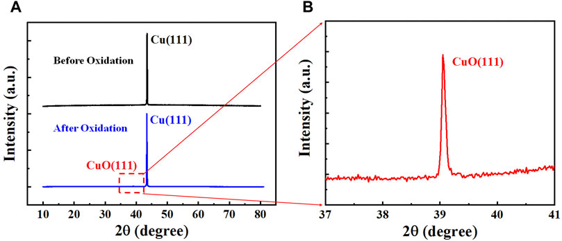
FIGURE 4. XRD characterization of copper foil. (A) XRD patterns obtained by a 2θ scan of the Cu (111) (∼43.3°) foil before (black) and after oxidation (red). (B) Zoom-in XRD pattern obtained by a 2θ scan, showing the CuO (111) peak at 38.7°.
After the copper oxidation, KPFM measurement has been performed to probe the electronic properties of monolayer h-BN in addition to the PF-TUNA mode (Chen et al., 2015a; Chen et al., 2017; Wan et al., 2017; Chen et al., 2015b; Wan et al., 2020; Wan et al., 2013; Wan et al., 2016). Figure 5A shows the band Gram of h-BN and CuO (111) based on the optical band gap Eg (OBG) estimated from the UV-visible absorption measurement and workfunction of CuO (111) reported in previous literatures (Sponza et al., 2018; Greiner and Lu, 2013; Singh and Mehta, 2014). Figure 5B shows the AFM image of the transferred h-BN nanoflakes on 300 nm thick SiO2/Si substrate, revealing a film thickness of 0.5 nm and confirming the monolayer nature of the sample. Figures 5C,F show the AFM topological images of the triangle and hexagonal monolayer h-BN on the CuO (111)/Cu substrate, respectively. In general, the lattice constant of CuO (a = 4.68 Å, b = 3.43 Å, c = 5.14 Å) is larger than that of Cu (a = b = c = 3.62 Å) (Varghese et al., 2016), which could further be verified by the XRD peak positions according to Bragg’s Law (see Supplementary Figure S6):
where n is a positive integer, λ is the wavelength of the incident wave, and d is the interplanar distance. Therefore, from the height line profiles taken from the AFM topological images in Figures 5C,F, the h-BN nanoflakes which cover the underlying Cu and prevent it from oxidation are 5–15 nm lower than the surrounding copper oxide as indicated in Figure 5I. This result is consistent with the SEM image as shown in Figure 1E. The contact potential energy difference (CPED) between the AFM tip and the local surface of h-BN and CuO is defined as (Rosenwaks et al., 2004; Wan et al., 2013; Chen et al., 2015a; Chen et al., 2015b; Wan et al., 2016)
where Wtip, Wh-BN, and WCuO are the work functions of the AFM conductive tip, h-BN, and CuO (111), respectively. Figures 5D,G display the corresponding KPFM maps of the triangle and hexagonal monolayer h-BN on the CuO substrate, revealing distinct color contrast between h-BN and CuO (111) regions, indicating that
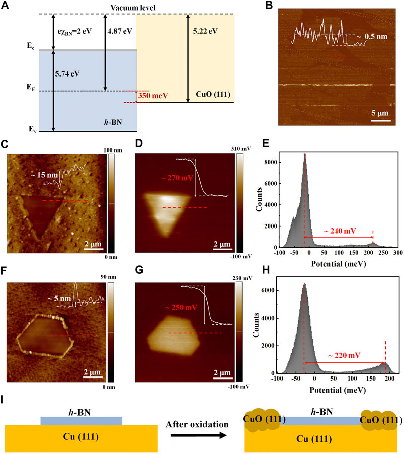
FIGURE 5. AFM KPFM measurements of monolayer h-BN nanoflakes on Cu after oxidation. (A) The band diagram of h-BN and CuO (111). (B) AFM image of transferred h-BN nanoflakes on SiO2/Si substrate. AFM height images of (C) triangle and (F) hexagonal monolayer h-BN nanoflakes on CuO (111). KPFM surface potential maps of (D) triangle and (G) hexagonal monolayer h-BN nanoflakes on CuO (111). The histogram distributions of the surface potentials for (E) triangle and (H) hexagonal monolayer h-BN nanoflakes on CuO (111). (I) Schematic of the h-BN/Cu before and after the oxidation.
Based on KPFM, the Fermi level of monolayer h-BN (∼4.95 eV), which lays in the middle of the bandgap, is 250–270 meV higher than that of CuO (111) (∼5.22 eV (Xia et al., 2018, Ahmad, 2016)). This result can be further confirmed by the histogram distributions as depicted in Figures 5E,H, where two prominent peaks can be observed. The larger distribution peak around −25 meV is attributed to the CuO (111) while the smaller one at 200 ± 20 meV is owning to the h-BN nanoflakes. The distinction (250–270 meV) between the inherent Fermi levels of h-BN and CuO (111) obtained by the KPFM maps is in good agreement with the theoretical values as shown in Figure 5A (Greiner and Lu, 2013; Singh and Mehta, 2014; Sponza et al., 2018). Overall, the KPFM results presented a direct visualization of the oxidation-resistance effect of h-BN and revealed the inherent Fermi level of h-BN.
In this work, monolayer h-BN flakes with various regular shapes have been synthesized by LPCVD using the copper-foil enclosure. The resistance of monolayer h-BN on Cu foil has been directly estimated by adopting the AFM PF-TUNA mode under an applied bias voltage of 10 V. A quantitative statistic of the TUNA current over a sample area of 20 μm × 20 µm showed that the resistance of monolayer h-BN was ∼440 GΩ, corresponding to a resistivity of ∼529 MΩ cm, which was consistent with the resistivity (∼501 MΩ cm) obtained from thick h-BN film. In addition to the PF-TUNA mode, KPFM measurement has been performed to quantitatively analyze the inherent Fermi level of h-BN (4.95 eV), which was close to the theoretical value (4.87 eV). Moreover, direct visualization of the oxidation-resistance effect of h-BN has been presented and the operating temperature can be further increased (Liu et al., 2013a). Our work demonstrates a direct estimation of the electronic properties for 2D materials on their initial growth substrate without an additional transfer process, avoiding any unwanted contaminations introduced during the transfer procedure. This quantitative analysis by state-of-the-art AFM techniques implies that monolayer h-BN can be used as an atomically thin, high-quality insulator for 2D electronics as well as a high-temperature antioxidation layer for electronic device applications.
CVD parameters for the growth monolayer h-BN; characterization of continuous h-BN films on the outside of the Cu-foil enclosure; SEM characterization of h-BN nanoflakes with growth time between 5 and15 min; optical image of h-BN films on the inner of Cu-foil enclosure and 300 nm thick SiO2/Si substrate; transfer of h-BN; XRD characterization of copper foil; the time dependence of the Z position, force, and current during one typical PeakForce Tapping cycle; AFM characterization of monolayer h-BN on Cu foil; electrical characterization of h-BN films.
The raw data supporting the conclusion of this article will be made available by the authors, without undue reservation.
XW, KC, and HC conceived and supervised the project. SD, YG, MG, SX, and XW contributed to sample preparation, materials characterization, device fabrication, measurements, and data analysis. KC performed the AFM measurements. XW, KC, and HC wrote the manuscript with input from other authors. All authors contributed to discussions.
This work was in part supported by the National Natural Science Foundation of China, particularly, via Grant No. 61804067; the Natural Science Foundation of Jiangsu Province, China under Grant Nos. BK20170193, BK 20170195; the E&I (Entrepreneurship and Innovation) Plan of Jiangsu Province under Grant No. 1256010241180240; the Fundamental Research Funds for the Central Universities of China under Grant No. JUSRP11746 and No. JUSRP51726B; the Six Talent Peaks Project in Jiangsu Province, under Grant No. DZXX-021; the Taihu Talent Plan in Wuxi City, under Grant No. 1256010241200320; and the 111 Project under Grant No. B12018. KC thanks the support by NSFC (Grant No. 51802360); the National Natural Science Foundation of Guangdong for Distinguished Young Scholars (Grant No. 2018B030306043); the Pearl River Talent Plan (Grant No. 2019QN01C109); the Science and Technology Program of Guangzhou (Grant No. 201904010449); the Key Cultivation Program for Young Teachers of Sun Yat-sen University (Grant No. 20lgzd13).
The authors declare that the research was conducted in the absence of any commercial or financial relationships that could be construed as a potential conflict of interest.
All claims expressed in this article are solely those of the authors and do not necessarily represent those of their affiliated organizations, or those of the publisher, the editors, and the reviewers. Any product that may be evaluated in this article, or claim that may be made by its manufacturer, is not guaranteed or endorsed by the publisher.
The Supplementary Material for this article can be found online at: https://www.frontiersin.org/articles/10.3389/fmats.2021.735344/full#supplementary-material
Ahmad, F. (2016). First Principle Calculation of Electronic, Optical Properties and Photocatalytic Potential of Cuo Surfaces. KnE Eng. 1, 1–7. doi:10.18502/keg.v0i0.504
Bai, C. (2000). Scanning Tunneling Microscopy and its Application. Springer-Verlag Berlin Heidelberg.
Bhaviripudi, S., Jia, X., Dresselhaus, M. S., and Kong, J. (2010). Role of Kinetic Factors in Chemical Vapor Deposition Synthesis of Uniform Large Area Graphene Using Copper Catalyst. Nano Lett. 10, 4128–4133. doi:10.1021/nl102355e
Britnell, L., Gorbachev, R. V., Jalil, R., Belle, B. D., Schedin, F., Katsnelson, M. I., et al. (2012). Electron Tunneling through Ultrathin Boron Nitride Crystalline Barriers. Nano Lett. 12, 1707–1710. doi:10.1021/nl3002205
Chen, K., Wan, X., Wen, J., Xie, W., Kang, Z., Zeng, X., et al. (2015). Electronic Properties of MoS2-WS2Heterostructures Synthesized with Two-step Lateral Epitaxial Strategy. ACS Nano. 9, 9868–9876. doi:10.1021/acsnano.5b03188
Chen, K., Wan, X., Xie, W., Wen, J., Kang, Z., Zeng, X., et al. (2015). Lateral Built-In Potential of Monolayer MoS2-WS2In-Plane Heterostructures by a Shortcut Growth Strategy. Adv. Mater. 27, 6431–6437. doi:10.1002/adma.201502375
Chen, K., Wan, X., and Xu, J. (2017). Epitaxial Stitching and Stacking Growth of Atomically Thin Transition-Metal Dichalcogenides (Tmdcs) Heterojunctions. Adv. Funct. Mater. 27, 1603884. doi:10.1002/adfm.201603884
Chen, T.-A., Chuu, C.-P., Tseng, C.-C., Wen, C.-K., Wong, H.-S. P., Pan, S., et al. (2020). Wafer-Scale Single-Crystal Hexagonal Boron Nitride Monolayers on Cu (111). Nature 579, 219–223. doi:10.1038/s41586-020-2009-2
Ci, L., Song, L., Jin, C., Jariwala, D., Wu, D., Li, Y., et al. (2010). Atomic Layers of Hybridized Boron Nitride and Graphene Domains. Nat. Mater. 9, 430–435. doi:10.1038/nmat2711
Coleman, J. N., Lotya, M., O'Neill, A., Bergin, S. D., King, P. J., Khan, U., et al. (2011). Two-Dimensional Nanosheets Produced by Liquid Exfoliation of Layered Materials. Science 331, 568–571. doi:10.1126/science.1194975
Dean, C. R., Young, A. F., Meric, I., Lee, C., Wang, L., Sorgenfrei, S., et al. (2010). Boron Nitride Substrates for High-Quality Graphene Electronics. Nat. Nanotech. 5, 722–726. doi:10.1038/nnano.2010.172
Duong, D. L., Han, G. H., Lee, S. M., Gunes, F., Kim, E. S., Kim, S. T., et al. (2012). Probing Graphene Grain Boundaries with Optical Microscopy. Nature 490, 235–239. doi:10.1038/nature11562
Fazen, P. J., Remsen, E. E., Beck, J. S., Carroll, P. J., Mcghie, A. R., and Sneddon, L. G. (1995). Synthesis, Properties, and Ceramic Conversion Reactions of Polyborazylene. A High-Yield Polymeric Precursor to Boron Nitride. Chem. Mater. 7, 1942–1956. doi:10.1021/cm00058a028
Frammelsberger, W., Benstetter, G., Kiely, J., and Stamp, R. (2007). C-AFM-based Thickness Determination of Thin and Ultra-thin SiO 2 Films by Use of Different Conductive-Coated Probe Tips. Appl. Surf. Sci. 253, 3615–3626. doi:10.1016/j.apsusc.2006.07.070
Greiner, M. T., and Lu, Z.-H. (2013). Thin-Film Metal Oxides in Organic Semiconductor Devices: Their Electronic Structures, Work Functions and Interfaces. Npg Asia Mater. 5, e55. doi:10.1038/am.2013.29
Hattori, Y., Taniguchi, T., Watanabe, K., and Nagashio, K. (2016). Anisotropic Dielectric Breakdown Strength of Single Crystal Hexagonal Boron Nitride. ACS Appl. Mater. Inter. 8, 27877–27884. doi:10.1021/acsami.6b06425
Hui, F., Fang, W., Leong, W. S., Kpulun, T., Wang, H., Yang, H. Y., et al. (2017). Electrical Homogeneity of Large-Area Chemical Vapor Deposited Multilayer Hexagonal Boron Nitride Sheets. ACS Appl. Mater. Inter. 9, 39895–39900. doi:10.1021/acsami.7b09417
Jiang, L., Shi, Y., Hui, F., Tang, K., Wu, Q., Pan, C., et al. (2017). Dielectric Breakdown in Chemical Vapor Deposited Hexagonal Boron Nitride. ACS Appl. Mater. Inter. 9, 39758–39770. doi:10.1021/acsami.7b10948
Kim, K. K., Hsu, A., Jia, X., Kim, S. M., Shi, Y., Dresselhaus, M., et al. (2012). Synthesis and Characterization of Hexagonal Boron Nitride Film as a Dielectric Layer for Graphene Devices. ACS Nano. 6, 8583–8590. doi:10.1021/nn301675f
Kim, K. K., Hsu, A., Jia, X., Kim, S. M., Shi, Y., Hofmann, M., et al. (2012). Synthesis of Monolayer Hexagonal Boron Nitride on Cu Foil Using Chemical Vapor Deposition. Nano Lett. 12, 161–166. doi:10.1021/nl203249a
Kubota, Y., Watanabe, K., Tsuda, O., and Taniguchi, T. (2007). Deep Ultraviolet Light-Emitting Hexagonal Boron Nitride Synthesized at Atmospheric Pressure. Science 317, 932–934. doi:10.1126/science.1144216
Lee, G.-H., Cui, X., Kim, Y. D., Arefe, G., Zhang, X., Lee, C.-H., et al. (2015). Highly Stable, Dual-Gated Mos2 Transistors Encapsulated by Hexagonal Boron Nitride with Gate-Controllable Contact, Resistance, and Threshold Voltage. ACS Nano. 9, 7019–7026. doi:10.1021/acsnano.5b01341
Lee, G.-H., Yu, Y.-J., Lee, C., Dean, C., Shepard, K. L., Kim, P., et al. (2011). Electron Tunneling through Atomically Flat and Ultrathin Hexagonal Boron Nitride. Appl. Phys. Lett. 99, 243114. doi:10.1063/1.3662043
Lee, K. H., Shin, H.-J., Lee, J., Lee, I.-y., Kim, G.-H., Choi, J.-Y., et al. (2012). Large-Scale Synthesis of High-Quality Hexagonal Boron Nitride Nanosheets for Large-Area Graphene Electronics. Nano Lett. 12, 714–718. doi:10.1021/nl203635v
Li, X., Magnuson, C. W., Venugopal, A., Tromp, R. M., Hannon, J. B., Vogel, E. M., et al. (2011). Large-Area Graphene Single Crystals Grown by Low-Pressure Chemical Vapor Deposition of Methane on Copper. J. Am. Chem. Soc. 133, 2816–2819. doi:10.1021/ja109793s
Liu, Z., Gong, Y., Zhou, W., Ma, L., Yu, J., Idrobo, J. C., et al. (2013). Ultrathin High-Temperature Oxidation-Resistant Coatings of Hexagonal Boron Nitride. Nat. Commun. 4, 2541. doi:10.1038/ncomms3541
Liu, Z., Ma, L., Shi, G., Zhou, W., Gong, Y., Lei, S., et al. (2013). In-Plane Heterostructures of Graphene and Hexagonal Boron Nitride with Controlled Domain Sizes. Nat. Nanotech. 8, 119–124. doi:10.1038/nnano.2012.256
McManus, D., Vranic, S., Withers, F., Sanchez-Romaguera, V., Macucci, M., Yang, H., et al. (2017). Water-Based and Biocompatible 2d Crystal Inks for All-Inkjet-Printed Heterostructures. Nat. Nanotech. 12, 343–350. doi:10.1038/nnano.2016.281
Pacilé, D., Meyer, J. C., Girit, Ç. Ö., and Zettl, A. (2008). The Two-Dimensional Phase of Boron Nitride: Few-Atomic-Layer Sheets and Suspended Membranes. Appl. Phys. Lett. 92, 133107. doi:10.1063/1.2903702
Qian, K., Tay, R. Y., Nguyen, V. C., Wang, J., Cai, G., Chen, T., et al. (2016). Hexagonal Boron Nitride Thin Film for Flexible Resistive Memory Applications. Adv. Funct. Mater. 26, 2176–2184. doi:10.1002/adfm.201504771
Ranjan, A., Raghavan, N., O’Shea, S. J., Mei, S., Bosman, M., Shubhakar, K., et al. (2018). Conductive Atomic Force Microscope Study of Bipolar and Threshold Resistive Switching in 2d Hexagonal Boron Nitride Films. Sci. Rep. 8, 2854. doi:10.1038/s41598-018-21138-x
Rosenwaks, Y., Shikler, R., Glatzel, T., and Sadewasser, S. (2004). Kelvin Probe Force Microscopy of Semiconductor Surface Defects. Phys. Rev. B 70, 085320. doi:10.1103/physrevb.70.085320
Scherzer, M., Girgsdies, F., Stotz, E., Willinger, M.-G., Frei, E., Schlögl, R., et al. (2019). Electrochemical Surface Oxidation of Copper Studied by In Situ Grazing Incidence X-Ray Diffraction. J. Phys. Chem. C. 123, 13253–13262. doi:10.1021/acs.jpcc.9b00282
Schillers, H., Medalsy, I., Hu, S., Slade, A. L., and Shaw, J. E. (2016). Peakforce Tapping Resolves Individual Microvilli on Living Cells. J. Mol. Recognit. 29, 95–101. doi:10.1002/jmr.2510
Shi, Y., Hamsen, C., Jia, X., Kim, K. K., Reina, A., Hofmann, M., et al. (2010). Synthesis of Few-Layer Hexagonal Boron Nitride Thin Film by Chemical Vapor Deposition. Nano Lett. 10, 4134–4139. doi:10.1021/nl1023707
Singh, B., and Mehta, B. R. (2014). Relationship between Nature of Metal-Oxide Contacts and Resistive Switching Properties of Copper Oxide Thin Film Based Devices. Thin Solid Films 569, 35–43. doi:10.1016/j.tsf.2014.08.030
Slattery, A., Shearer, C., Shapter, J., Blanch, A., Quinton, J., and Gibson, C. (2018). Improved Application of Carbon Nanotube Atomic Force Microscopy Probes Using Peakforce Tapping Mode. Nanomaterials 8, 807. doi:10.3390/nano8100807
Song, L., Ci, L., Lu, H., Sorokin, P. B., Jin, C., Ni, J., et al. (2010). Large Scale Growth and Characterization of Atomic Hexagonal Boron Nitride Layers. Nano Lett. 10, 3209–3215. doi:10.1021/nl1022139
Sponza, L., Amara, H., Attaccalite, C., Latil, S., Galvani, T., Paleari, F., et al. (2018). Direct and Indirect Excitons in Boron Nitride Polymorphs: A Story of Atomic Configuration and Electronic Correlation. Phys. Rev. B. 98, 125206. doi:10.1103/physrevb.98.125206
Stehle, Y. Y., Voylov, D., Vlassiouk, I. V., Lassiter, M. G., Park, J., Sharma, J. K., et al. (2017). Effect of Polymer Residues on the Electrical Properties of Large-Area Graphene-Hexagonal Boron Nitride Planar Heterostructures. Nanotechnology 28, 285601. doi:10.1088/1361-6528/aa7589
Steinborn, C., Herrmann, M., Keitel, U., Schönecker, A., Räthel, J., Rafaja, D., et al. (2013). Correlation between Microstructure and Electrical Resistivity of Hexagonal Boron Nitride Ceramics. J. Eur. Ceram. Soc. 33, 1225–1235. doi:10.1016/j.jeurceramsoc.2012.11.024
Varghese, J. J., Trinh, Q. T., and Mushrif, S. H. (2016). Insights into the Synergistic Role of Metal-Lattice Oxygen Site Pairs in Four-Centered C-H Bond Activation of Methane: the Case of CuO. Catal. Sci. Technol. 6, 3984–3996. doi:10.1039/c5cy01784j
Wan, X., Chen, K., Chen, Z., Xie, F., Zeng, X., Xie, W., et al. (2017). Controlled Electrochemical Deposition of Large-Area Mos2 on Graphene for High-Responsivity Photodetectors. Adv. Funct. Mater. 27, 1603998. doi:10.1002/adfm.201603998
Wan, X., Chen, K., Du, J., Liu, D., Chen, J., Lai, X., et al. (2013). Enhanced Performance and Fermi-Level Estimation of Coronene-Derived Graphene Transistors on Self-Assembled Monolayer Modified Substrates in Large Areas. J. Phys. Chem. C. 117, 4800–4807. doi:10.1021/jp309549z
Wan, X., Chen, K., Xie, W., Wen, J., Chen, H., and Xu, J.-B. (2016). Quantitative Analysis of Scattering Mechanisms in Highly Crystalline CVD MoS2through a Self-Limited Growth Strategy by Interface Engineering. Small 12, 438–445. doi:10.1002/smll.201502392
Wan, X., Miao, X., Yao, J., Wang, S., Shao, F., Xiao, S., et al. (2021). In Situ Ultrafast and Patterned Growth of Transition Metal Dichalcogenides from Inkjet‐Printed Aqueous Precursors. Adv. Mater. (Weinheim, Ger). 33, 2100260. doi:10.1002/adma.202100260
Wan, X., Li, H., Chen, K., and Xu, J. (2020). Towards Scalable Fabrications and Applications of 2d Layered Material-Based Vertical and Lateral Heterostructures. Chem. Res. Chin. Univ. 36, 525–550. doi:10.1007/s40242-020-0200-5
Wang, L., Xu, X., Zhang, L., Qiao, R., Wu, M., Wang, Z., et al. (2019). Epitaxial Growth of a 100-Square-Centimetre Single-Crystal Hexagonal Boron Nitride Monolayer on Copper. Nature 570, 91–95. doi:10.1038/s41586-019-1226-z
Xia, W., Luo, M., Zeng, X., Yang, J., Dong, J., Xu, Q., et al. (2018). Different Annealing Atmosphere Gases on the Growth and Photocurrent Performance of Cuo Films Grown on Fto Substrate. ACS Omega. 3, 11354–11361. doi:10.1021/acsomega.8b01529
Keywords: h-BN, resistance, surface potential, chemical vapor deposition, PeakForce TUNA AFM, KPFM (kelvin probe force microscope)
Citation: Deng S, Gu Y, Wan X, Gao M, Xu S, Chen K and Chen H (2021) Probing Electronic Properties of CVD Monolayer Hexagonal Boron Nitride by an Atomic Force Microscope. Front. Mater. 8:735344. doi: 10.3389/fmats.2021.735344
Received: 02 July 2021; Accepted: 16 July 2021;
Published: 17 August 2021.
Edited by:
Qiaoliang Bao, Soochow University, ChinaCopyright © 2021 Deng, Gu, Wan, Gao, Xu, Chen and Chen. This is an open-access article distributed under the terms of the Creative Commons Attribution License (CC BY). The use, distribution or reproduction in other forums is permitted, provided the original author(s) and the copyright owner(s) are credited and that the original publication in this journal is cited, in accordance with accepted academic practice. No use, distribution or reproduction is permitted which does not comply with these terms.
*Correspondence: Xi Wan, eHdhbkBqaWFuZ25hbi5lZHUuY24=; Kun Chen, Y2hlbms2OUBtYWlsLnN5c3UuZWR1LmNu; Huanjun Chen, Y2hlbmhqOEBtYWlsLnN5c3UuZWR1LmNu
Disclaimer: All claims expressed in this article are solely those of the authors and do not necessarily represent those of their affiliated organizations, or those of the publisher, the editors and the reviewers. Any product that may be evaluated in this article or claim that may be made by its manufacturer is not guaranteed or endorsed by the publisher.
Research integrity at Frontiers
Learn more about the work of our research integrity team to safeguard the quality of each article we publish.