 Jinyu Ruan1
 Tiandong Zhang
95% of researchers rate our articles as excellent or good
Learn more about the work of our research integrity team to safeguard the quality of each article we publish.
Find out more
ORIGINAL RESEARCH article
Front. Mater. , 15 September 2021
Sec. Thin Solid Films
Volume 8 - 2021 | https://doi.org/10.3389/fmats.2021.732186
This article is part of the Research Topic Thin Film Technology: Processing, Properties and Applications View all 4 articles
Ferroelectric multilayer films attract great attention for a wide variation of applications. The synergistic effect by combining different functional layers induces distinctive electrical properties. In this study, ferroelectric BaZr0.2Ti0.8O3/PbZr0.52Ti0.48O3/BaZr0.2Ti0.8O3 (BZT/PZT/BZT) multilayer thin films are designed and fabricated by using the magnetron sputtering method, and a LaNiO3 (LNO) seed layer is introduced. The microstructures and electrical properties of the BZT/PZT/BZT films with and without the LNO seed layer are systematically studied. The results show that the BZT/PZT/BZT/LNO thin film exhibits much lower surface roughness and a preferred (100)-orientation growth, with the growth template and tensile stress provided by the LNO layer. Moreover, an enhanced dielectric constant, decreased dielectric loss, and improved ferroelectric properties are achieved in BZT/PZT/BZT/LNO thin films. This work reveals that the seed layer can play an important role in improving the microstructure and properties of ferroelectric multilayer films.
Ferroelectric thin films have been widely studied for several decades, which exhibit excellent dielectric, piezoelectric, and ferroelectric properties, which can be widely used as telecommunications, sensors, transducers, and so on. Representative ferroelectric materials such as Pb(Zr,Ti)O3 (Damjanovic, 1998; Muralt, 2008; Palukurua et al., 2014), Pb(Mg1/3Nb2/3)O3-PbTiO3 (Feng et al., 2011; Crossley et al., 2016), Ba(Zr,Ti)O3 (Cao and Li, 2009; Fan et al., 2010; Luo et al., 2013), (Bi1/2Na1/2)TiO3 (Feng et al., 2016; Lin et al., 2016), and BiFeO3 (Rojac1 et al., 2017; Campanini et al., 2018) have been intensively investigated and well-developed. With the increasing awareness of environmental protection, many studies strive to replace Pb-based thin films with Pb-free ones. Although progress has been made in Pb-free films, the electrical properties in most cases are still inferior to those of Pb-based ones.
Constructing multilayer thin films may be a compromise strategy to reduce the usage of lead and retain the outstanding characteristics of lead materials. Moreover, a novel physical phenomenon and exceptional properties may be achieved by combining the lead-free films with lead-based ones. For example, the BiFeO3/PbZr0.5Ti0.5O3 multilayer films exhibit not only reduced leakage current but also enhanced dielectric properties compared with pure BiFeO3 films (Li et al., 2005). Dielectric anomaly was also observed in PbZr0.2Ti0.8O3/SrTiO3 (ferroelectric/paraelectric) bilayer films due to the polarization mismatch. A maximum dielectric constant could be obtained when the layer thickness ratio reached a critical value (Khassaf et al., 2016). Besides, compositionally multilayer thin films (Damodaran et al., 2017a) and heterostructure thin films (Damodaran et al., 2017b; Zhang et al., 2017) also exhibit outstanding electrical properties. In addition, in bilayer films composed of a ferromagnetic NiFe or CoFe2O4 layer and ferroelectric Pb(Zr,Ti)O3 layer, a remarkable magnetoelectric effect was obtained (Li et al., 2016; Ramírez-Camacho et al., 2017).
It is well-known that the growth orientations and electrical properties of ferroelectric thin films are very sensitive to the stress from the substrate, seed layer, buffer layer, or interfacial layer. For example, BaZr0.2Ti0.8O3 (BZT) films with a preferred (100) orientation can be obtained by using a La0.7Sr0.3MnO3 bottom layer (Tang et al., 2006) or LaNiO3 (LNO) seed layer (LiZhang et al., 2015) on Pt/Ti/SiO2/Si substrates in which the dielectric and piezoelectric properties were substantially improved. Specifically, LNO was widely used to regulate the microstructure and growth orientation (Li et al., 2010; Zhu et al., 2016) and to optimize the piezoelectric coefficient (LiZhang et al., 2014; LiZhang et al., 2015), polarization behavior (Hou et al., 2015), and photovoltaic current (Cheng, et al., 2020) of ferroelectric films. In this study, BaZr0.2Ti0.8O3 (BZT)/PbZr0.52Ti0.48O3 (PZT)/BZT multilayer thin films are constructed for performance enhancement, and the LNO is chosen as a seed layer for the film growth. The effects of LNO seed layer on the microstructure and electrical properties are systematically studied in this work.
An LNO seed layer of ∼10 nm in thickness was grown on Pt (111)/Ti/SiO2/Si substrates by a sol-gel method, as reported in our previous study (LiZhang et al., 2015). The raw materials were lanthanum nitrate [La(NO3)3] and nickel acetate [Ni(CH3COO)2]. La(NO3)3 and Ni(CH3COO)2 were dissolved and refluxed for 30 min in the heated 2-methoxyethanol solvent, and the concentration of the solution was adjusted to 0.05 mol/L. After the precursor solution was aged for 24 h, the LNO layer was spin-coated on the Pt (111)/Ti/SiO2/Si substrates, followed by pyrolysis at 400°C for 3 min, and then annealing at 750°C for 30 min. BZT and PZT thin films were then grown on the LNO/Pt (111)/Ti/SiO2/Si substrates with a magnetron sputtering method. A base pressure of 5 × 10⁻⁵ Pa was achieved before sputtering, and the Ar-to-O2 flow ratio was 3:1 during film growth. The top and bottom BZT layers are ∼150 nm in thickness, and the PZT interlayer is ∼200 nm in thickness. Finally, the prepared BZT/PZT/BZT and BZT/PZT/BZT/LNO thin films were annealed at 750°C for 30 min to enhance crystallization.
The crystalline structures of the thin films were analyzed by a Philips X′ pert X-ray diffractometer (XRD) with Cu Kɑ radiation generated at 40 kV and 40 mA. The cross-section micrographs of the thin films were obtained by using scanning electron microscopy (SEM, Helios Nanolab600i), and the film surface morphology was characterized by an atomic force microscope (AFM). Piezoelectric response was detected by a piezoelectric force microscope (PFM). For further electrical property measurements, platinum electrodes with a diameter of 200 μm were deposited by DC magnetron sputtering. The ferroelectric properties and leakage current were characterized by a Radiant Precision Workstation Ferroelectric Measurement System. The frequency and temperature dependent dielectric properties were measured on a precision impedance analyzer (Agilent 4294A), with an AC voltage of 500 mV.
The XRD measurement shows a pure perovskite phase of the films (Figure 1A). It is found that the BZT/PZT/BZT/LNO thin films possess preferred (100)-oriented growth, while the BZT/PZT/BZT films without the LNO seed layer do not exhibit an obvious crystal orientation preference. The XRD rocking curve (ω scan) of the BZT/PZT/BZT/LNO film exhibits a full width at a half maximum (FWHM) of 6.9° (the inset of Figure 1A). This small FWHM value reflects the strong orientation preference induced by the LNO seed layer. There are no diffraction peaks of the LNO seed layer due to its small thickness, consistent with our previous studies (LiZhang et al., 2015). To study the stress state in the BZT/PZT/BZT thin films, the grazing incidence X-ray diffraction (GIXD) method (Hou et al., 2015) was employed, and the results are shown in Figures 1B,C. According to the equation of ψ = θ-ω (θ is incident angle, ω is the grazing incident angle, and ψ is the included angle between the normal direction of films and diffraction crystal plane), ψ can be obtained by changing the ω value. Furthermore, the slightly changed θ value means the variation of the interplanar crystal spacing di, which can be calculated by the Bragg’s equation 2disinθ = λ, [here, d0 is the interpalne spacing of stress-free specimen and (di-d0)/d0 corresponds the crystal lattice strain]. It should be noted that there is a linear relationship between the (di-d0)/d0 and sin2ψ. (For detailed derivation process, refer the previous reports (Wang et al., 2010).) The increased incident angle ω corresponds to the increasing penetration depth of X-ray. Therefore, the strain distribution behavior along the normal direction in the films can be revealed by the GIXD method with different ω values. In this work, the GIXD peaks of the (200) planes are shown in Figures 1B,C, respectively, for the BZT/PZT/BZT and BZT/PZT/BZT/LNO thin films. It can be seen that the diffraction peak is almost unchanged for the BZT/PZT/BZT films, which, as a comparison, exhibits an increased two theta with the increasing ω in the BZT/PZT/BZT/LNO films. It means that the LNO seed layer induces tensile stress in the BZT/PZT/BZT thin films, leading to an increased interplanar spacing di, as shown in Figure 1D.
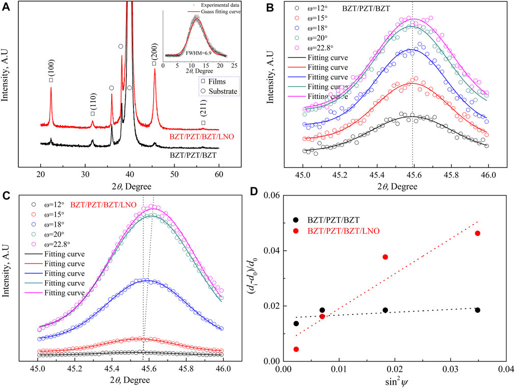
FIGURE 1. XRD patterns of the BZT/PZT/BZT multilayer films. (A) θ–2θ scan patterns; the inset is the rocking curve patterns. (B, C) GIXD of (001) peaks of BZT/PZT/BZT and BZT/PZT/BZT/LNO multilayer films. (D) Dependence of the interplanar crystal spacing on sin2ψ.
Figure 2 shows the surface morphology of the films. The films fabricated by magnetron sputtering exhibit island growth characteristics. SEM images show that the grain size is about 1 μm, with some fine grains of ∼100 nm distributed sporadically between the adjacent large grains (Figures 2A,B). In order to obtain more detailed surface information, AFM characterization was employed, and the results are given in Figures 2C,D. It can be clearly found that a more compact and smoother surface structure is obtained in the BZT/PZT/BZT/LNO films. The film roughness was evaluated by the root-mean-square (RMS) values derived from the AFM measurement, which are 16.7 and 7.4 nm for the BZT/PZT/BZT and BZT/PZT/BZT/LNO thin films, respectively. The results indicate that the LNO seed layer is beneficial to improve the film quality and to reduce the surface roughness.
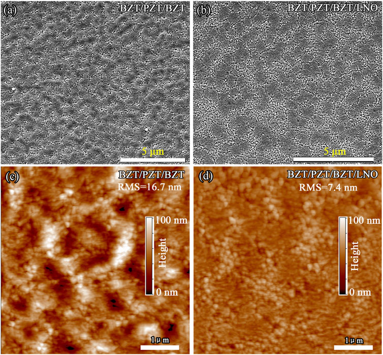
FIGURE 2. Surface morphology images of the BZT/PZT/BZT and BZT/PZT/BZT/LNO thin films. (A, B) SEM images; (C, D) AFM images.
Cross-sectional SEM images of the films are shown in Figure 3. It can be seen that the BZT/PZT/BZT/LNO thin film possesses a much denser microstructure than that of the BZT/PZT/BZT thin film without the LNO seed layer. Some voids between adjacent grains can be seen in the BZT/PZT/BZT thin film, which is much more obviously seen in the backscattered electron (BSE) images, as given in Figures 3B,D. The total thickness of the films is verified to be ∼500 nm, with the thickness of the top and bottom BZT layers of about 150 nm, and the PZT interlayer of about 200 nm. The interface between BZT and PZT can be clearly observed due to the different atomic numbers of Ba and Pb, and thus the varied contrast in the BSE image. The LNO seed layer is too thin to observe from the SEM images, whose thickness was estimated to be ∼10 nm via the X-ray reflectivity method (LiZhang et al., 2015).
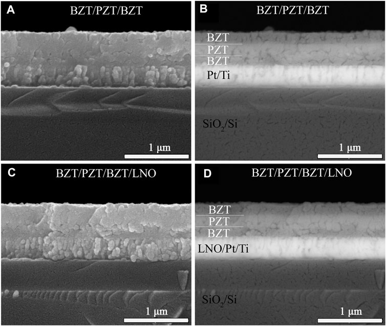
FIGURE 3. Cross-sectional images of the BZT/PZT/BZT and BZT/PZT/BZT/LNO thin films. (A, C) SEM images; (B, D) BSE images.
Since dielectric properties are very important for ferroelectric thin films, the dependence of dielectric properties on the measurement frequency and temperature is investigated, and the results are given in Figure 4. It can be found that the dielectric constant is notably improved by introducing an LNO seed layer into the BZT/PZT/BZT film. The dielectric constants are 451.7 and 598.6, respectively, for the BZT/PZT/BZT and BZT/PZT/BZT/LNO thin films at 1 kHz. As shown in Figure 4B, the dielectric loss of the BZT/PZT/BZT/LNO thin film at higher frequencies is lower than that of BZT/PZT/BZT/LNO thin films. The enhanced dielectric constant and the decreased dielectric loss can be ascribed to the improved film quality and polarization capability by inserting the LNO seed layer, which is consistent with the results of previous reports (Wu and Shy, 2000; Gao et al., 2008). The temperature-dependent dielectric properties of the films are presented in Figures 4C,D. It can be observed that both the BZT/PZT/BZT and the BZT/PZT/BZT/LNO thin films possess a wide peak of dielectric constant, which may correspond to the transition from the rhombohedral phase to the cubic phase of BZT (Lee et al., 2005; Xu et al., 2015). Such broad peaks could also link to the diffuse phase transitions due to the substrate clamping effect (Setter, et al., 2006; Tong, et al., 2011). Besides, the BZT/PZT/BZT/LNO film maintains lower and more stable dielectric loss values as the temperature increases, which is also associated with the higher quality and less defective microstructure of the film with the LNO seed layer.
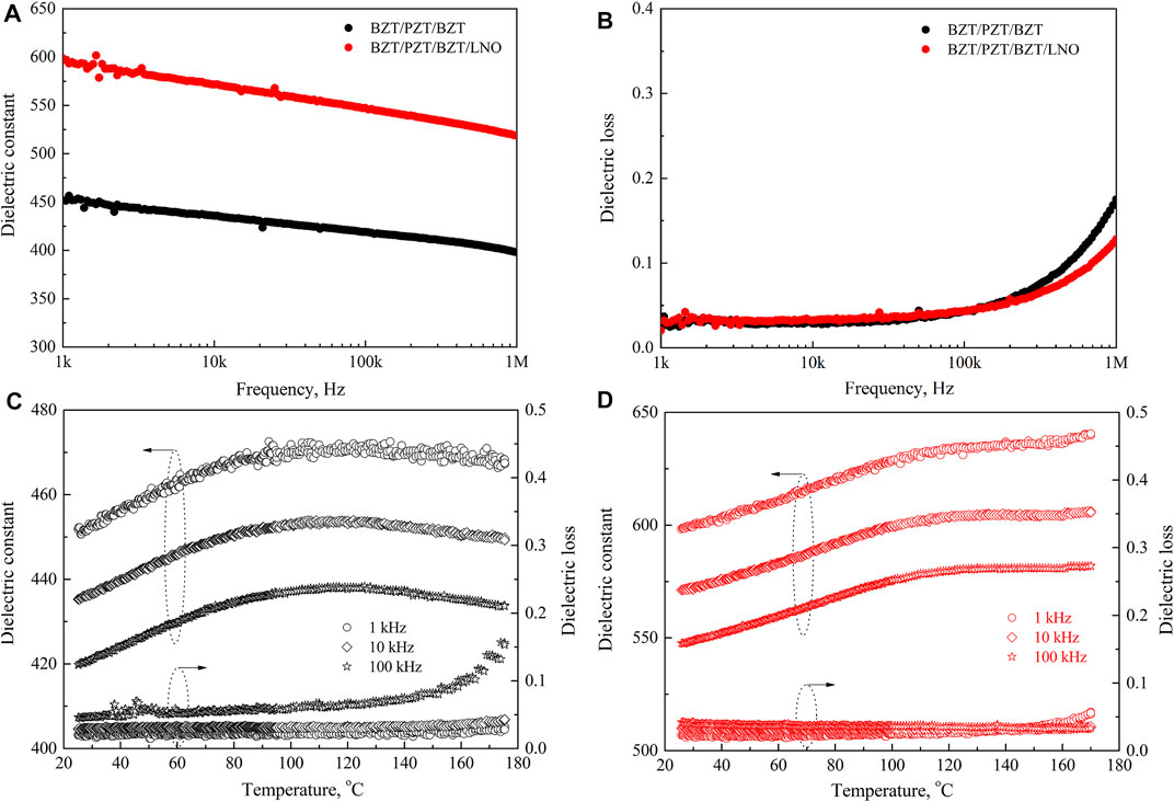
FIGURE 4. Dependence of dielectric properties on measured frequency and temperature. (A) Dielectric constant. (B) Dielectric loss. (C) BZT/PZT/BZT. (D) BZT/PZT/BZT/LNO.
Ferroelectric properties of the films are investigated by measuring hysteresis polarization-voltage loops. As given in Figure 5A, the hysteresis loops of the BZT/PZT/BZT thin film are not completely closed, and an obvious gap can be seen at the negative branch as the applied voltage decreases to zero. This phenomenon may be correlated with the leakage current or conduction loss, which further leads to the asymmetric coercive voltage (Vc) values. As a comparison, it can be noticed that the hysteresis loops of the BZT/PZT/BZT/LNO film is almost closed after the voltage cycle, indicating a lower leakage current. It should be noted that the obviously asymmetric coercive voltage values still exist in the BZT/PZT/BZT/LNO thin film, with the + Vc of 16.4 V and–Vc of –8.4 V. It was reported that the loop offset along the voltage axis can be induced by the asymmetric electrode structure of thin films (Lee et al., 2005; Wong and Shin, 2005). In addition, the interfacial charge in the multilayer films and the existence of built-in electric field may also lead to the asymmetrical characteristics of hysteresis loops (Karthik et al., 2013; Agar et al., 2015).
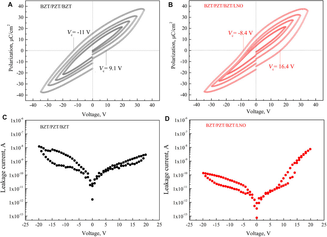
FIGURE 5. Hysteresis loops and leakage current with different applied voltages. (A, C) BZT/PZT/BZT thin films. (B, D) BZT/PZT/BZT/LNO thin films.
Figures 5C,D show the leakage current of the thin films at different voltages. The leakage current of the BZT/PZT/BZT/LNO film is generally lower than that of the BZT/PZT/BZT film. Besides, in the BZT/PZT/BZT/LNO thin film, the leakage current exhibits an unsymmetrical characteristic, which is higher at positive bias voltages. A possible reason may be the asymmetric electrodes that lead to different interfacial Schottky barrier heights and induce the unsymmetrical characteristics of IV curve (Shen et al., 2014; Fan et al., 2015; Chen et al., 2020).
To further study the effects of the LNO seed layer on the polarization behavior of thin films, piezoelectric force microscopy (PFM) was employed to directly observe the polarization reversal behavior, based on the evolution of piezoelectric response. A positive voltage and a negative voltage were applied sequentially on the BZT/PZT/BZT/LNO film. A 3,000-nm × 3,000-nm area at the center of the selected region was first poled by +20 V voltage (Figure 6A), and then a 1,000-nm × 1,000-nm area at the center was poled by an inversed –20 V voltage to study the polarization reversal (Figure 6B). It should be pointed out that the voltage was applied between the bottom electrode and PFM tip, and the tip was grounded. Finally, the PFM signals of the 5,000 nm × 5,000 nm area were scanned after removing the voltage (Figure 6C). Because the piezoelectric response signal is proportional to the out-of-plane polarization of the film, the bright regions correspond to upward polarization, and dark regions to downward polarization. In Figure 6D, one can find that the intensity of the positive piezoelectric response is stronger than that of the negative piezoelectric response, meaning that thin films are easier to be polarized when a positive polarization voltage is applied.
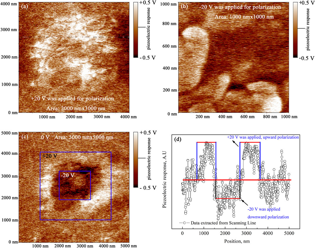
FIGURE 6. PFM images of the BZT/PZT/BZT/LNO thin film. (A) + 20 V polarization voltage. (B) −20 V polarization voltage. (C) Scanning after voltage was removed. (D) Piezoelectric response extracted from a scanning line in Fig. (C).
In this study, BZT/PZT/BZT/LNO thin films were fabricated by combining magnetron sputtering and sol-gel methods. The results show that the (100) preferred orientation growth of the BZT/PZT/BZT thin film is induced by introducing an LNO seed layer, with which a denser microstructure and lower surface roughness are achieved. More importantly, the dielectric constant increases and the dielectric loss decreases with the insertion of the LNO layer, accompanied by a diffuse phase transition behavior. Besides, asymmetric hysteresis loops and leakage current curves are found in the BZT/PZT/BZT/LNO thin film, which can be attributed to the LNO seed layer that may cause different polarization abilities under different electric field directions. The PFM measurement also supports the above deduction. This work provides an effective way to improve the microstructure and electrical properties of ferroelectric multilayer thin films by introducing an LNO seed layer.
The original contributions presented in the study are included in the article/Supplementary Material; further inquiries can be directed to the corresponding authors.
JR: writing and investigation. CY: material synthesis. TZ: investigation and conceptualization. HP: writing and conceptualization.
The authors gratefully acknowledge support from the Outstanding Youth Fund of Heilongjiang Province (No. YQ2020E031). China Postdoctoral Science Foundation (No.2021T140166)
The authors declare that the research was conducted in the absence of any commercial or financial relationships that could be construed as a potential conflict of interest.
All claims expressed in this article are solely those of the authors and do not necessarily represent those of their affiliated organizations, or those of the publisher, the editors, and the reviewers. Any product that may be evaluated in this article, or claim that may be made by its manufacturer, is not guaranteed or endorsed by the publisher.
Agar, J. C., Damodaran, A. R., Velarde, G. A., Pandya, S., Mangalam, R. V. K., and Martin, L. W. (2015). Complex Evolution of Built-in Potential in Compositionally-Graded PbZr1-xTixO3 Thin Films. ACS Nano 9, 7332–7342. doi:10.1021/acsnano.5b02289
Campanini, M., Erni, R., Yang, C. H., Ramesh, R., and Rossell, M. D. (2018). Periodic Giant Polarization Gradients in Doped BiFeO3 Thin Films. Nano Lett. 18, 717–724. doi:10.1021/acs.nanolett.7b03817
Cao, H.-X., and Li, Z.-Y. (2009). Electrocaloric effect in BaTiO3 thin films. J. Appl. Phys. 106, 094104. doi:10.1063/1.3253736
Chen, A., Zhang, W., Dedon, L. R., Chen, D., Khatkhatay, F., MacManus‐Driscoll, J. L., et al. (2020). Couplings of polarization with interfacial deep trap and schottky interface controlled ferroelectric memristive switching. Adv. Funct. Mater. 30, 2000664. doi:10.1002/adfm.202000664
Cheng, S., Fan, Z., Rao, J., Hong, L., Huang, Q., Tao, R., et al. (2020). Highly controllable and silicon-compatible ferroelectric photovoltaic synapses for neuromorphic computing. iScience 23, 101874. doi:10.1016/j.isci.2020.101874
Crossley, S., Usui, T., Nair, B., Kar-Narayan, S., Moya, X., Hirose, S., et al. (2016). Direct electrocaloric measurement of 0.9Pb(Mg1/3Nb2/3)O3-0.1PbTiO3 films using scanning thermal microscopy. Appl. Phys. Lett. 108, 032902. doi:10.1063/1.4938758
Damjanovic, D. (1998). Ferroelectric, dielectric and piezoelectric properties of ferroelectric thin films and ceramics. Rep. Prog. Phys. 61, 1267–1324. doi:10.1088/0034-4885/61/9/002
Damodaran, A. R., Clarkson, J. D., Hong, Z., Liu, H., Yadav, A. K., Nelson, C. T., et al. (2017). Phase coexistence and electric-field control of toroidal order in oxide superlattices. Nat. Mater 16, 1003–1009. doi:10.1038/NMAT4951
Damodaran, A. R., Pandya, S., Qi, Y., Hsu, S.-L., Liu, S., Nelson, C., et al. (2017). Large polarization gradients and temperature-stable responses in compositionally-graded ferroelectrics. Nat. Commun. 8, 14961. doi:10.1038/ncomms14961
Fan, Y., Yu, S., Sun, R., Li, L., Yin, Y., and Du, R. (2010). Microstructure and electrical properties of Ba0.7Sr0.3(Ti1−xZrx)O3 thin films prepared on copper foils with sol-gel method. Thin Solid Films 518, 3610–3614. doi:10.1016/j.tsf.2009.09.051
Fan, Z., Xiao, J., Yao, K., Zeng, K., and Wang, J. (2015). Ferroelectric polarization relaxation in Au/Cu2O/ZnO/BiFeO3/Pt heterostructure. Appl. Phys. Lett. 106, 102902. doi:10.1063/1.4914883
Feng, C., Yang, C. H., Geng, F. J., Lv, P. P., and Yao, Q. (2016). Microstructure and electrical properties mediated by defects in Na 0.5 Bi 0.5 Ti 0.98 Mn 0.02 O 3 thin film under different annealing atmospheres. J. Eur. Ceram. Soc. 36, 527–532. doi:10.1016/j.jeurceramsoc.2015.10.015
Feng, Z., Shi, D., Zeng, R., and Dou, S. (2011). Large electrocaloric effect of highly (100)-oriented 0.68PbMg1/3Nb2/3O3-0.32PbTiO3 thin films with a Pb(Zr0.3Ti0.7)O3/PbOx buffer layer. Thin Solid Films 519, 5433–5436. doi:10.1016/j.tsf.2011.02.069
Gao, L. N., Song, S. N., Zhai, J. W., Yao, X., and Xu, Z. K. (2008). Effects of buffer layers on the orientation and dielectric properties of Ba(Zr0.20Ti0.80)O3 thin films prepared by sol-gel method. J. Cryst. Growth 310, 1245–1249. doi:10.1016/j.jcrysgro.2007.12.015
Hou, Y. F., Zhang, T. D., Li, W. L., Cao, W. P., Yu, Y., Xu, D., et al. (2015). Self-polarization induced by lattice mismatch and defect dipole alignment in (001) BaTiO3/LaNiO3 polycrystalline film prepared by magnetron sputtering at low temperature. RSC Adv. 5, 61821–61827. doi:10.1039/c5ra07337e
Karthik, J., Mangalam, R. V. K., Agar, J. C., and Martin, L. W. (2013). Large built-in electric fields due to flexoelectricity in compositionally graded ferroelectric thin films. Phys. Rev. B 87, 024111. doi:10.1103/PhysRevB.87.024111
Khassaf, H., Khakpash, N., Vijayan, S., Aindow, M., and Alpay, S. P. (2016). Electrostatically driven dielectric anomaly in mesoscopic ferroelectric-paraelectric bilayers. Acta Materialia 105, 68–74. doi:10.1016/j.actamat.2015.12.023
Lee, H. N., Christen, H. M., Chisholm, M. F., Rouleau, C. M., and Lowndes, D. H. (2005). Strong polarization enhancement in asymmetric three-component ferroelectric superlattices. Nature 433, 395–399. doi:10.1038/nature0324810.1038/nature03261
Li, Y.-C., Pan, D.-F., WuLi, J. Y.-B., Li, Y.-b., Wang, G.-h., Liu, J.-M., et al. (2016). Manipulating the exchange bias effect of Pb(Zr0.52Ti0.48)O3/CoFe2O4/NiO heterostructural films by electric fields. Appl. Phys. Lett. 109, 172904. doi:10.1063/1.4966545
Li, Y. W., Shen, Y. D., Yue, F. Y., Hu, Z. G., Ma, X. M., Chu, J. H., et al. (2010). Preparation and characterization of BiFeO3/LaNiO3 heterostructure films grown on silicon substrate. J. Cryst. Growth 312, 617–620. doi:10.1016/j.jcrysgro.2009.11.058
Li, Y. W., Sun, J. L., Chen, J., Meng, X. J., and Chu, J. H. (2005). Structural, ferroelectric, dielectric, and magnetic properties of BiFeO3∕Pb(Zr0.5,Ti0.5)O3 multilayer films derived by chemical solution deposition. Appl. Phys. Lett. 87, 182902. doi:10.1063/1.2120907
Lin, Q., Ding, R., Li, Q., Tay, Y. Y., Wang, D., Liu, Y., et al. (2016). Large Piezoelectricity and Ferroelectricity in Mn‐Doped (Bi 0.5 Na 0.5 )TiO 3 ‐BaTiO 3 Thin Film Prepared by Pulsed Laser Deposition. J. Am. Ceram. Soc. 99, 2347–2353. doi:10.1111/jace.14227
LiZhang, W. L. T. D., Zhang, T. D., Hou, Y. F., Zhao, Y., Xu, D., Cao, W. P., et al. (2014). Giant piezoelectric properties of BZT-0.5BCT thin films induced by nanodomain structure. RSC Adv. 4, 56933–56937. doi:10.1039/c4ra08280j
LiZhang, W. L. T. D., Zhang, T. D., Xu, D., Hou, Y. F., Cao, W. P., and Fei, W. D. (2015). LaNiO3 seed layer induced enhancement of piezoelectric properties in (100)-oriented (1−x)BZT-xBCT thin films. J. Eur. Ceram. Soc. 35, 2041–2049. doi:10.1016/j.jeurceramsoc
Luo, B. C., Wang, D. Y., Duan, M. M., and Li, S. (2013). Orientation-dependent piezoelectric properties in lead-free epitaxial 0.5BaZr0.2Ti0.8O3-0.5Ba0.7Ca0.3TiO3 thin films. Appl. Phys. Lett. 103, 122903. doi:10.1063/1.4821918
Muralt, P. (2008). Recent progress in materials issues for piezoelectric MEMS. J. Am. Ceram. Soc. 91, 1385–1396. doi:10.1088/0034-4885/61/9/00210.1111/j.1551-2916.2008.02421.x
Palukuru, V. K., Lappalainen, J., Puustinen, J., Kangaspuoskari, M., and Huotari, J. (2014). Dielectric and Tunability Properties of Nanostructured Nd-modified Pb(ZrxTi1-x)O3Thin Films up to Microwave Frequencies. Ferroelectrics 465, 20–27. doi:10.1080/00150193.2014.893735
Ramírez-Camacho, M. C., Sánchez-Valdés, C. F., Gervacio-Arciniega, J. J., Font, R., Ostos, C., Bueno-Baques, D., et al. (2017). Room temperature ferromagnetism and ferroelectricity in strained multiferroic BiFeO3 thin films on La0.7Sr0.3MnO3/SiO2/Si substrates. Acta Materialia 128, 451–464. doi:10.1063/1.2120907
Rojac, T., Bencan, A., Drazic, G., Sakamoto, N., Ursic, H., Jancar, B., et al. (2017). Domain-wall conduction in ferroelectric BiFeO3 controlled by accumulation of charged defects. Nat. Mater 16, 322–327. doi:10.1038/NMAT4799
Setter, N., Damjanovic, D., Eng, L., Fox, G., Gevorgian, S., Hong, S., et al. (2006). Ferroelectric thin films: Review of materials, properties, and applications. J. Appl. Phys. 100, 051606. doi:10.1063/1.2336999
Shen, L. M., Tang, X. G., Liu, Q. X., Jiang, Y. P., Wang, Y. G., and Li, W. P. (2014). Room temperature ferroelectric properties and leakage current characterics of Bi2 FeMnO6 /SrTiO3 bilayered thin films by chemical solution deposition. Phys. Status Solidi A. 211, 1499–1502. doi:10.1002/pssa.201330617
Tang, X. G., Liu, Q. X., Jiang, Y. P., Zheng, R. K., and Chan, H. L. W. (2006). Enhanced dielectric properties of highly (100)-oriented Ba(Zr,Ti)O[sub 3] thin films grown on La[sub 0.7]Sr[sub 0.3]MnO[sub 3] bottom layer. J. Appl. Phys. 100, 114105. doi:10.1063/1.2393010
Tong, S., Narayanan, M., Ma, B., Koritala, R. E., Liu, S., Balachandran, U., et al. (2011). Effect of dead layer and strain on the diffuse phase transition of PLZT relaxor thin films. Acta Materialia 59, 1309–1316. doi:10.1016/j.actamat.2010.10.063
Wang, J. N., Li, W. L., Feng, B., Liu, C. Q., Li, X. L., Sun, Q., et al. (2010). Residual stress of Pb(ZrxTi1−x)O3 films with mixed textures. J. Alloys Comp. 506, 167–171. doi:10.1016/j.jallcom.2010.06.170
Wong, C. K., and Shin, F. G. (2005). A possible mechanism of anomalous shift and asymmetric hysteresis behavior of ferroelectric thin films. Appl. Phys. Lett. 86, 042901. doi:10.1063/1.1853520
Wu, T.-B., and Shy, H.-J. (2000). Deposition and properties of highly (100)-oriented barium titanate thin films on LaNiO3 electrode. Ceramics Int. 26, 599–603. doi:10.1016/S0272-8842(99)00103-0
Xu, X., Yuan, G., Xu, B., Yin, J., Liu, J., and Liu, Z. (2015). Influence of the Strain on Dielectric and Ferroelectric Properties of 0.5BaZr0.2 Ti0.8 O3 -0.5Ba0.7 Ca0.3 TiO3. J. Am. Ceram. Soc. 98, 2823–2828. doi:10.1111/jace.13677
Zhang, Y.-J., Chen, J.-H., Li, L.-L., Ma, J., Nan, C.-W., and Lin, Y.-H. (2017). Ferroelectric strain modulation of antiferromagnetic moments in Ni/NiO ferromagnet/antiferromagnet heterostructures. Phys. Rev. B 95, 174420. doi:10.1103/PhysRevB.95.174420
Keywords: magnetron sputtering, multilayer films, seed layer, microstructure, electrical property
Citation: Ruan J, Yin C, Zhang T and Pan H (2021) Effects of LaNiO3 Seed Layer on the Microstructure and Electrical Properties of Ferroelectric BZT/PZT/BZT Thin Films. Front. Mater. 8:732186. doi: 10.3389/fmats.2021.732186
Received: 28 June 2021; Accepted: 03 August 2021;
Published: 15 September 2021.
Edited by:
Weiwei Li, University of Cambridge, United KingdomReviewed by:
Renlu Han, Ningbo University, ChinaCopyright © 2021 Ruan, Yin, Zhang and Pan. This is an open-access article distributed under the terms of the Creative Commons Attribution License (CC BY). The use, distribution or reproduction in other forums is permitted, provided the original author(s) and the copyright owner(s) are credited and that the original publication in this journal is cited, in accordance with accepted academic practice. No use, distribution or reproduction is permitted which does not comply with these terms.
*Correspondence: Tiandong Zhang, dGR6aGFuZ0BocmJ1c3QuZWR1LmNu; Hao Pan, aGFvLnBhbkBudHUuZWR1LnNn
Disclaimer: All claims expressed in this article are solely those of the authors and do not necessarily represent those of their affiliated organizations, or those of the publisher, the editors and the reviewers. Any product that may be evaluated in this article or claim that may be made by its manufacturer is not guaranteed or endorsed by the publisher.
Research integrity at Frontiers
Learn more about the work of our research integrity team to safeguard the quality of each article we publish.