 Caroline E. Reilly
 Stacia Keller2
- 1Department of Materials, University of California, Santa Barbara, Santa Barbara, CA, United States
- 2Department of Electrical and Computer Engineering, University of California, Santa Barbara, Santa Barbara, CA, United States
This review will cover recent work on InN quantum dots (QDs), specifically focusing on advances in metalorganic chemical vapor deposition (MOCVD) of metal-polar InN QDs for applications in optoelectronic devices. The ability to use InN in optoelectronic devices would expand the nitrides system from current visible and ultraviolet devices into the near infrared. Although there was a significant surge in InN research after the discovery that its bandgap provided potential infrared communication band emission, those studies failed to produce an electroluminescent InN device in part due to difficulties in achieving p-type InN films. Devices utilizing InN QDs, on the other hand, were hampered by the inability to cap the InN without causing intermixing with the capping material. The recent work on InN QDs has proven that it is possible to use capping methods to bury the QDs without significantly affecting their composition or photoluminescence. Herein, we will discuss the current state of metal-polar InN QD growth by MOCVD, focusing on density and size control, composition, relaxation, capping, and photoluminescence. The outstanding challenges which remain to be solved in order to achieve InN infrared devices will be discussed.
Introduction
Since InN was found to have a bandgap of 0.7 eV in 2002, the nitrides community has claimed that the III-nitrides system can span from the near infrared all the way to the ultraviolet (Davydov et al., 2002; Wu, 2009). While the high energy side has seen considerable research, the low energy side has been largely left to other III-V materials. While there is a new push for high indium content materials for red-emitting devices, devices in the infrared have been the subject of less research in the nitrides. However, there are some significant potential benefits of nitride-based infrared optoelectronics and related devices (Mi and Zhao, 2015; Nötzel, 2017). The nitrides system promises better thermal behavior compared to arsenide and phosphide based systems by virtue of the wide bandgap of GaN and the large band offset in the GaN/InN system (Van De Walle and Neugebauer, 2003). Carriers can then stay confined within the active region and issues such as secondary lasing or carrier overshoot are mitigated. Furthermore, dislocation movement–which is a concern in other III-V semiconductors–does not significantly affect the nitrides system (Ishida et al., 1977; Schwartz, 1985; Callahan et al., 2018).
Although InN-based IR devices are attractive in theory, they have presented a considerable materials challenge. Where there is a lattice mismatch between GaAs and InAs of about 7%, the lattice mismatch in the GaN/InN system is over 10%. This leads to extremely thin critical thicknesses before the onset of relaxation and the formation of dislocations. There are also large discrepancies between the growth temperatures of GaN and InN, particularly for metalorganic chemical vapor deposition (MOCVD). Typical growth temperatures for high quality GaN are above 1,000°C whereas InN is grown below 700°C in order to limit decomposition or sublimation of the InN. In the case where GaN would be grown on top of In-content material, a high growth temperature can cause intermixing between the (In,Ga)N and GaN (Ku et al., 2007; Wang et al., 2008; Li et al., 2013). These challenges lead to difficulties in growing sufficiently thick InN layer as well as difficulties in capping any InN with GaN.
MOCVD studies of InN have largely focused on the growth of nanostructures such as quantum dots or dashes (QDs) due in part to the natural formation of these structures under large lattice mismatch conditions. Studies via molecular beam epitaxy (MBE) have shown evidence for stress driven surface reconstructions resulting in the formation of In0.33Ga0.67N instead of pure InN quantum wells in (0001) InN/GaN multi-layer structures (Suski et al., 2014; Chèze et al., 2017). Some MBE studies report monolayer-thick strained InN layers and, while these layers are useful for digital alloy applications (Yoshikawa et al., 2007; Yoshikawa et al., 2008; Gorczyca et al., 2018), they have limited usage in infrared optoelectronics, as their very thin nature typically leads to a blue shift resulting in emission in the visible range of the electromagnetic spectrum (Wu et al., 2009).
By MOCVD, thick planar InN layers have been demonstrated (Bhuiyan et al., 2003; Ruffenach et al., 2010), however there are additional benefits to the use of QDs in optoelectronic devices. In comparison to quantum wells (QWs), QDs have additional in-plane confinement which can localize carriers. This can reduce the movement of carriers to defects or dislocations which are present outside of any given QD, mitigating nonradiative recombination of carriers (Gérard et al., 1996; Mi et al., 2009). In lasers, QDs have been additionally shown to reduce transparency current and improve temperature stability (Arakawa and Sakaki, 1982; Asada et al., 1986).
This review will focus on recent work in MOCVD of metal-polar InN QDs on GaN for the purposes of light-emitting devices. Significant work on InN QDs has been conducted by MBE, where lower temperatures are more common for nitride growth (Ng et al., 2002; Nörenberg et al., 2002; Zhou et al., 2006; Soto Rodriguez et al., 2013; Soto Rodriguez et al., 2015). However, scaling up the growth by MBE is less practical and MOCVD is the industry standard for optoelectronic devices in the nitrides. Work on crystal orientations other than the (0001) plane of GaN has also been conducted but to a lesser extent and will be outside the scope of the current review (Yoshikawa et al., 2005; Yang et al., 2016; Bi et al., 2018; Lund et al., 2018; Reilly et al., 2019b).
Density and Size Control
The ability to control QD size is a critical step toward optoelectronic devices with precise wavelengths and emission linewidths. As the dimensions of the InN are reduced to those of QDs, the wavelength of emission blue shifts dramatically (Yoshikawa et al., 2008). This can be beneficial by providing a handle on the wavelength, but this effect can also cause an undesirable emission broadening when the QDs are not all the same size. While each individual QD has very sharp emission, the emission FWHM of the device will be related to the size distribution of the QDs. Typically, the size and density are linked when adjusting the growth parameters. Shape and aspect ratio are also factors that can vary, with most InN QDs being truncated hexagonal pyramids of varied aspect ratios, as seen in Figure 1 (Briot et al., 2003; Ku et al., 2007; Bonef et al., 2020). Depending on the specific application, different sizes, shapes, and densities may be required.
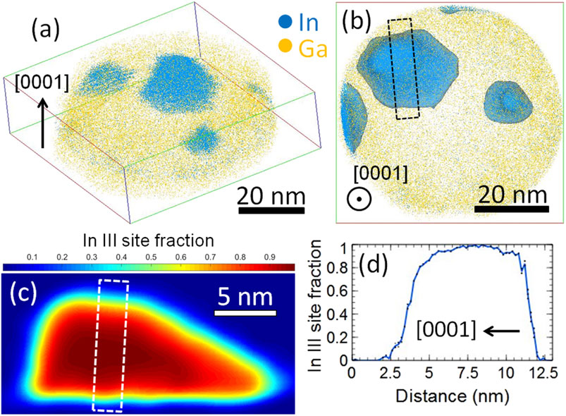
FIGURE 1. Atom probe tomography data of InN QDs on GaN grown by MOCVD. (A) 3D reconstruction, (B) top view with a 50% In iso-concentration surface, (C) 2D side view extracted from dashed region in (B), and (D) 1D concentration profile of In extracted from dashed region in (C). Detection rate was 0.005 atoms pulse−1 and detection efficiency was 37%, with more information in the references. From Bonef et al., Appl. Phys. Express 13, 065005 (2020). Copyright (2020) The Japan Society of Applied Physics (Bonef et al., 2020; Bonef et al., 2017).
The majority of studies reporting InN QD growth are on c-plane (0001) GaN using trimethylindium (TMIn) or triethylindium (TEIn) as the group III precursor and NH3 as the group V precursor. Results using alternative group V precursors (dimethylhydrazine and tertiarybutylhydrazine) showed no growth of InN and were not further considered herein (Ruffenach et al., 2009). Although there are some differences in the literature as far as the precise size and densities of InN QDs at various temperatures are concerned, general trends hold. Growth parameters such as growth time, V/III ratio, and temperature all affect the dot size, shape, and density. Some of these parameters control secondary factors such as the growth rate and adatom mobilities, where higher growth rates or lower adatom mobilities typically lead to smaller and denser QDs when the nominal thickness–the thickness of a complete layer with the same amount of material as in the QDs–is kept constant.
The nominal thickness of the QDs is typically directly related to the growth time and can either be reported as the expected value, based on a calibrated growth rate and growth time, or it can be a calculated value, for instance by assuming some size and shape for the QDs and using the density to find a nominal thickness. At very short growth times, the calculated nominal thickness from the QDs may not correspond to the expected nominal thickness due to the establishment of a wetting layer (Bonef et al., 2020). At longer growth times, a linear relationship has been seen between the calculated nominal thickness and growth time (Meissner et al., 2009). As growth time increases, initially both dot height and diameter increase until the diameter stops increasing while the height continues to increase (Meissner et al., 2009; Reilly et al., 2020b). The dot density typically increases sharply in the early stages of dot growth during the nucleation process, up to densities on the order of 1010 cm−2 (T = 550 °C; GR = of 0.25 Å/s) (Bonef et al., 2020). At longer growth times, little change occurs in the density as the dots continue to increase in size (Meissner et al., 2009; Reilly et al., 2020b).
Despite the low temperatures necessary for InN growth, the surface catalytic decomposition of NH3 is sufficient at high enough V/III ratios. At low V/III ratios, In droplets form and no InN growth may occur (Briot et al., 2003). As the NH3 cracking efficiency decreases with decreasing deposition temperatures, higher NH3 supplies become necessary to maintain a sufficient V/III ratio. At a growth temperature of 550 °C, a V/III ratio of 7,150 resulted in In droplets while a V/III ratio of 15,000 produced InN (Briot et al., 2003). A modulated flow scheme, in which TMIn and NH3 were supplied intermittently and the NH3 background flow during TMIn flow was varied, showed InN dots decreasing in diameter and increasing in density as the background NH3 flow was increased (Ke et al., 2006). The height-to-diameter ratio was seen to increase with increasing NH3 flow, related to the decreased lateral and increased vertical diffusion of surface adatoms with higher V/III ratios (Ke et al., 2006).
The deposition temperature has a significant impact on both growth rate and surface adatom mobility. At very low temperatures the growth rate is determined by the kinetics of the precursor decomposition, followed at intermediate temperatures by a regime where the growth rate is transport limited and tends to stay relatively constant. However, at higher temperatures InN will decompose or desorb, causing the growth rate to decrease with increasing temperature (Meissner et al., 2008). The surface adatom mobility also increases at higher temperatures, leading to longer diffusion lengths on the surface and less dense QDs. Across many studies, it has been seen that increasing temperatures led to less dense, taller, and wider QDs (Figures 2A–D) (Briot et al., 2003; Ruffenach et al., 2005; Meissner et al., 2008; Reilly et al., 2020b). Changing the growth temperature over a 100 °C range can lead to density changes of two orders of magnitude, giving a large degree of control over the density. However, decreased growth temperatures can lead to problems with capping the quantum dots, as will be discussed in Photoluminescence and Capping.
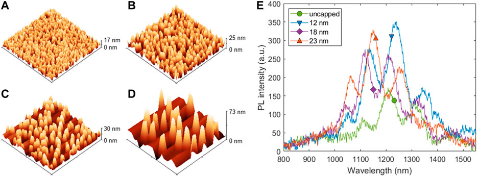
FIGURE 2. (A)–(D) InN QDs in 3D atomic force micrographs; (1.5 μm)2 scans for QDs with growth temperatures of (A) 515, (B) 550, (C) 565, and (D) 600°C. (E) Room temperature photoluminescence (PL) from InN QDs, excited with a 780 nm laser, with indicated GaN cap thicknesses. From Reilly et al., Phys. Status Solidi B 257, 1900508 (2020). © 2019 WILEY‐VCH Verlag GmbH & Co. KGaA, Weinheim (Reilly et al., 2020).
Composition and Relaxation
With phase separation of InGaN being a known problem (Ho and Stringfellow, 1996), bimodal compositional distributions have been observed in high In containing InGaN QDs (El-Masry et al., 1998; Tessarek et al., 2011; Reilly et al., 2019a). Intermixing of InN with the GaN surrounding the InN QDs is a concern as well. At the very low growth temperatures of InN, intermixing would be expected to play less of a problem than at higher temperatures. For uncapped InN QDs, X-ray diffraction (XRD) has shown the InN composition of the QDs to be very close to 100% In, with little to no Ga incorporation (Briot et al., 2003; Meissner et al., 2009; Reilly et al., 2020b). In addition, recent advances in capping InN with LT GaN have also revealed little Ga incorporation into capped InN QDs by XRD, photoluminescence (PL), and atom probe tomography (APT) (Bonef et al., 2020; Reilly et al., 2020b). Figure 1 presents APT data of capped InN QDs, in which the center of the dots are observed to be 100% InN (Figure 1C) and relatively sharp interfaces with the surrounding GaN exist (Figure 1D), as discussed further in Photoluminescence and Capping (Bonef et al., 2020).
The XRD data additionally highlight the strain state of the InN QDs. As may be expected due to the high lattice mismatch between GaN and InN, the InN QDs are seen to be nearly fully relaxed. Transmission electron microscopy (TEM) studies have confirmed the relaxed nature of the InN QDs as well as confirming the presence of a misfit dislocation network at the interface between the underlying GaN and the InN QDs (Lozano et al., 2005; Lozano et al., 2007; Ivaldi et al., 2011; Bonef et al., 2020). The dislocations are largely contained at the interface and do not propagate into the QDs (Lozano et al., 2005). The growth of QDs and the relaxed nature of the InN has been seen for very low nominal thicknesses of under one monolayer (Meissner et al., 2008; Bonef et al., 2020).
This early onset of QD growth in addition to the relaxed nature of the dots indicated a Volmer-Weber growth mode of InN QDs on GaN by MOCVD (Meissner et al., 2009). Investigations of InN films with a nominal thickness well below one monolayer showed a thin, incomplete InGaN layer which developed prior to the onset of InN QD growth (Bonef et al., 2020). This incomplete layer was visible by both TEM and APT, with quantification by APT showing that, during the initial nucleation of QDs, the InGaN layer became thicker and the proportion of material incorporating into the wetting layer decreased over time. No conventional wetting layer was observed, providing further evidence for Volmer-Weber growth (Bonef et al., 2020).
Photoluminescence and Capping
For InN QDs to be incorporated as the active region in standard LED and laser diode structures, the dots must be buried underneath additional material, either p-type or n-type. In keeping with the standard structure of nitride LEDs, the doped regions would be GaN. Until recently, studies have seen that the QDs degrade through decomposition and intermixing effects upon capping with GaN (Ku et al., 2007; Ivaldi et al., 2011). At higher GaN capping temperatures, which provide higher GaN quality, this effect was enhanced further. Infrared PL was seen to drastically decrease as the GaN capping temperature was increased, with both PL and XRD indicating the degradation of the InN and the formation of InGaN. In these previous studies, the InN QDs were deposited at around 700 °C, and the GaN cap layers were grown between 600 and 730 °C (Ku et al., 2007). Under all conditions, intermixing was observed. Various other capping schemes employing lower growth temperatures, InGaN capping, or two-step capping were also unsuccessful in capping the InN QDs without degradation (Ivaldi et al., 2011). In one study, in which the InN composition was thought to be maintained using lower temperature capping, the shape and strain state of the QDs were negatively impacted (Lozano et al., 2006).
In a more recent study, however, the IR luminescence of InN QDs (room temperature, 780 nm laser excitation) was preserved after the deposition of GaN cap layers with varying thickness, with little to no blue shift or loss of intensity (Figure 2E) (Reilly et al., 2020b). In the PL, the multiple peaks were due to the Fabry-Pérot effect. This suggested that the InN QDs were relatively unaffected by the GaN cap, which was grown at the same temperature as the QDs. AFM indicated conformal GaN cap growth, with QDs remaining visible even after deposition of GaN caps which were thicker than the dot height. XRD showed a slight peak shift indicative of some Ga incorporation into the capped InN QDs, however this effect was significantly less than seen in previous studies (Reilly et al., 2020b; Ivaldi et al., 2011). This may have been due, in part, to the use of atmospheric pressure MOCVD suppressing the movement of In. APT studies on similar samples, with even thicker GaN cap layers, showed no Ga incorporation in the center of the QDs (Figure 1) (Bonef et al., 2020). The GaN cap was free of indium after an initial drop-off at the interface between the QDs and the cap. Interfaces remained sharp despite the thick cap growth and the size and shape of the QDs remained similar to that measured via AFM prior to GaN cap growth.
Discussion
The existing work on InN QDs by MOCVD has mapped out the growth space such that the size, shape, and density of QDs can be tailored for specific applications by varying parameters such as growth time, V/III ratio, temperature, and precursor flows. Reported densities on the order of 1010 cm−2 can be useful for applications such as LEDs and laser diodes, whereas lower densities might be useful for single-photon emission applications. These dots were also grown at high enough temperatures to allow for GaN capping at the same temperature without significant PL loss. For applications in LEDs and laser diodes, further optimizations toward reducing the dot heights, to the order of 5 nm, while growing at high enough temperatures to allow for good quality GaN are necessary. Reducing the diameters of the QDs would also provide benefits if a truly zero-dimensional regime could be reached. However, as the benefit of QDs being less susceptible to threading dislocations can be achieved even with dot diameters too large to provide quantum confinement in-plane, the diameter of the QDs is less of a concern than the height. Additionally, maintaining or increasing the dot density to provide a large emitting area can enhance the benefits associated with the use of QDs.
Although decreasing the size of the QDs should improve the device properties, the decrease in dot size causes an increase in quantum confinement and therefore a blue shift in the emission properties. This causes the emission of the QDs to be outside of the 1,550 nm communication band of interest, although there are still uses for infrared emission at shorter wavelengths. Engineering around this effect is nontrivial, as the desire for smaller QDs directly conflicts with the blue shift which occurs. Other issues also arise for these smaller sizes, including the increasingly strong dependence of emission wavelength on the QD size. Extremely precise control over the size is then necessary to achieve a target wavelength, such that deviations from the average QD size can significantly broaden the FWHM of the emission.
Other considerations toward achieving full LED and laser structures relate to the nature of the GaN cap itself. The conformal nature of the GaN cap and concerns related to the quality of the capping layers–in particular the elevated impurity incorporation in lower temperature GaN films–pose problems toward successful devices (Ivaldi et al., 2011; Reilly et al., 2020b). Planarization of the top layer would be desired in order to stack multiple dot layers and for the processing of devices. The desired planarization may be achieved as dot size is reduced, such that smaller dots are more easily covered. The GaN cap layer quality concerns may be addressed via alternative growth schemes, such as flow-modulation epitaxy, which has been seen to also reduce impurity incorporation (Reilly et al., 2020a). Using GaN flow-modulation epitaxy conditions for the capping of InN QDs at the InN QD growth temperature was also shown to retain the XRD signal of the InN after capping of QDs (Reilly et al., 2020a).
In conclusion, significant advances have been achieved toward the demonstration of an InN QD electroluminescence device. Dot size and density can be tuned through a variety of growth parameters, with densities useful for many applications. Achieving small enough InN QDs is still of some concern, especially due to the blue-shift associated with the decrease in size. However, the ability to cap InN QDs without intermixing or loss of PL overcomes one of the main barriers of previous studies. With further advances in low temperature growth of GaN, a nitride based infrared light-emitting device should be near on the horizon.
Author Contributions
CR is the first author and corresponding author. SK, SN, and SD have also contributed to the writing of this work.
Conflict of Interest
The authors declare that the research was conducted in the absence of any commercial or financial relationships that could be construed as a potential conflict of interest.
Acknowledgments
This work was supported by the Solid State Lighting and Energy Electronics Center at the University of California, Santa Barbara.
References
Arakawa, Y., and Sakaki, H. (1982). Multidimensional quantum well laser and temperature dependence of its threshold current. Appl. Phys. Lett. 40, 939–941. doi:10.1063/1.92959
Asada, M., Miyamoto, Y., and Suematsu, Y. (1986). Gain and the threshold of three-dimensional quantum-box lasers. IEEE J. Quan. Electron. 22, 1915–1921. doi:10.1109/jqe.1986.1073149
Bhuiyan, A. G., Hashimoto, A., and Yamamoto, A. (2003). Indium nitride (InN): a review on growth, characterization, and properties. J. Appl. Phys. 94, 2779–2808. doi:10.1063/1.1595135
Bi, Z., Ek, M., Stankevic, T., Colvin, J., Hjort, M., Lindgren, D., et al. (2018). Self-assembled InN quantum dots on side facets of GaN nanowires. J. Appl. Phys. 123, 164302. doi:10.1063/1.5022756
Bonef, B., Catalano, M., Lund, C., Denbaars, S. P., Nakamura, S., Mishra, U. K., et al. (2017). Indium segregation in N-polar InGaN quantum wells evidenced by energy dispersive X-ray spectroscopy and atom probe tomography. Appl. Phys. Lett. 110, 143101. doi:10.1063/1.4979786
Bonef, B., Reilly, C. E., Wu, F., Nakamura, S., DenBaars, S. P., Keller, S., et al. (2020). Quantitative investigation of indium distribution in InN wetting layers and dots grown by metalorganic chemical vapor deposition. Appl. Phys. Express 13, 065005. doi:10.1063/1.120639
Briot, O., Maleyre, B., and Ruffenach, S. (2003). Indium nitride quantum dots grown by metalorganic vapor phase epitaxy. Appl. Phys. Lett. 83, 2919–2921. doi:10.1063/1.2152110
Callahan, P. G., Haidet, B. B., Jung, D., Seward, G. G. E., and Mukherjee, K. (2018). Direct observation of recombination-enhanced dislocation glide in heteroepitaxial GaAs on silicon. Phys. Rev. Mater. 2, 081601. doi:10.1103/physrevmaterials.2.081601
Chèze, C., Feix, F., Anikeeva, M., Schulz, T., Albrecht, M., Riechert, H., et al. (2017). In/GaN(0001)- (r3 x r3)R30deg adsorbate structure as a template for embedded (In, Ga)N/GaN monolayers and short-period superlattices. Appl. Phys. Lett. 110, 072104. doi:10.1063/1.4976198
Davydov, V. Y., Klochikhin, A. A., V Emtsev, V., Ivanov, S. V., Vekshin, V. V., Bechstedt, F., et al. (2002). Band Gap of InN and In-Rich in x Ga 1-x N alloys (0.36 < x < 1). Phys. Status Sol. 230, R4–R6. doi:10.1002/1521-3951(200204)230:2<r4::aid-pssb99994>3.0.co;2-z
El-Masry, N. A., Piner, E. L., Liu, S. X., and Bedair, S. M. (1998). Phase separation in InGaN grown by metalorganic chemical vapor deposition. Appl. Phys. Lett. 72, 40–42. doi:10.35848/1882-0786/ab9167
Gérard, J. M., Cabrol, O., and Sermage, B. (1996). InAs quantum boxes: highly efficient radiative traps for light emitting devices on Si. Appl. Phys. Lett. 68, 3123–3125. doi:10.1063/1.115798
Gorczyca, I., Suski, T., Christensen, N. E., and Svane, A. (2018). Theoretical study of nitride short period superlattices. J. Phys. Condens. Matter 30, 063001. doi:10.1088/1361-648x/aaa2ae
Ho, I.-H., and Stringfellow, G. B. (1996). Solid phase immiscibility in GaInN. Appl. Phys. Lett. 69, 2701–2703. doi:10.1063/1.117683
Ishida, K., Kamejima, T., and Matsui, J. (1977). Nature of ⟨ 110 ⟩ dark-line defects in degraded (GaAl) As-GaAs double-heterostructure lasers. Appl. Phys. Lett. 31, 397–399. doi:10.1063/1.89705
Ivaldi, F., Meissner, C., Domagala, J., Kret, S., Pristovsek, M., Högele, M., et al. (2011). Influence of a GaN cap layer on the morphology and the physical properties of embedded self-organized InN quantum dots on GaN(0001) grown by metal-organic vapour phase epitaxy. Jpn. J. Appl. Phys. 50, 031004. doi:10.1016/j.jcrysgro.2008.07.066
Ke, W. C., Lee, L., Chen, C. Y., Tsai, W. C., Chang, W. H., Chou, W. C., et al. (2006). Impacts of ammonia background flows on structural and photoluminescence properties of InN dots grown on GaN by flow-rate modulation epitaxy. Appl. Phys. Lett. 89, 263117. doi:10.1063/1.2425038
Ku, C. S., Chou, W. C., and Lee, M. C. (2007). Optical investigations of InN nanodots capped by GaN at different temperatures. Appl. Phys. Lett. 90, 132116. doi:10.1063/1.2716347
Li, Z. C., Liu, J. P., Feng, M. X., Zhou, K., Zhang, S. M., Wang, H., et al. (2013). Effects of matrix layer composition on the structural and optical properties of self- organized InGaN quantum dots. J. Appl. Phys. 114, 093105. doi:10.1063/1.4820935
Lozano, J. G., Sánchez, A. M., García, R., González, D., Araújo, D., Ruffenach, S., et al. (2005). Nucleation of InN quantum dots on GaN by metalorganic vapor phase epitaxy. Appl. Phys. Lett. 87, 263104. doi:10.1063/1.2152110
Lozano, J. G., Sánchez, A. M., García, R., Gonzalez, D., Briot, O., and Ruffenach, S. (2006). Misfit relaxation of InN quantum dots: effect of the GaN capping layer. Appl. Phys. Lett. 88, 151913. doi:10.1063/1.2195642
Lozano, J. G., Sánchez, A. M., García, R., Ruffenach, S., Briot, O., and González, D. (2007). Strain relief analysis of InN quantum dots grown on GaN. Nanoscale Res. Lett. 2, 442–446. doi:10.1007/s11671-007-9080-6
Lund, C., Catalano, M., Wang, L., Wurm, C., Mates, T., Kim, M., et al. (2018). Metal-organic chemical vapor deposition of N-polar InN quantum dots and thin films on vicinal GaN. J. Appl. Phys. 123, 055702. doi:10.1063/1.5009904
Meissner, C., Ploch, S., Leyer, M., Pristovsek, M., and Kneissl, M. (2008). Indium nitride quantum dot growth modes in metalorganic vapour phase epitaxy. J. Cryst. Growth 310, 4959–4962. doi:10.1016/j.jcrysgro.2008.07.066
Meissner, C., Ploch, S., Pristovsek, M., and Kneissl, M. (2009). Volmer-Weber growth mode of InN quantum dots on GaN by MOVPE. Phys. Status Sol. C 6, S545–S548. doi:10.1002/pssc.200880872
Mi, Z., Yang, J., Bhattacharya, P., Qin, G., and Ma, Z. (2009). High-performance quantum dot lasers and integrated optoelectronics on Si. Proc. IEEE 97, 1239–1249. doi:10.1109/jproc.2009.2014780
Mi, Z., and Zhao, S. (2015). Extending group-III nitrides to the infrared: recent advances in InN. Phys. Status Solidi Basic Res. 252, 1050–1062. doi:10.1002/pssb.201451628
Ng, Y. F., Cao, Y. G., Xie, M. H., Wang, X. L., and Tong, S. Y. (2002). Growth mode and strain evolution during InN growth on GaN(0001) by molecular-beam epitaxy. Appl. Phys. Lett. 81, 3960–3962. doi:10.1063/1.1523638
Nörenberg, C., Oliver, R. A., Martin, M. G., Allers, L., Castell, M. R., and Briggs, G. A. D. (2002). Stranski-Krastanov growth of InN nanostructures of GaN studied by RHEED, STM and AFM. Phys. Status Sol. 194, 536–540. doi:10.1002/1521-396X(200212)194:2<536::AID-PSSA536>3.0.CO;2-B
Nötzel, R. (2017). InN/InGaN quantum dot electrochemical devices: new solutions for energy and health. Natl. Sci. Rev. 4, 184–195. doi:10.1093/nsr/nww101
Reilly, C. E., Bonef, B., Nakamura, S., Speck, J. S., DenBaars, S. P., and Keller, S. (2019a). Characterization of InGaN quantum dots grown by metalorganic chemical vapor deposition. Semicond. Sci. Technol. 34, 125002. doi:10.1088/1361-6641/ab4b93
Reilly, C. E., Lund, C., Nakamura, S., Mishra, U. K., DenBaars, S. P., and Keller, S. (2019b). Infrared luminescence from N-polar InN quantum dots and thin films grown by metal organic chemical vapor deposition. Appl. Phys. Lett. 114, 241103. doi:10.1063/1.5109734
Reilly, C. E., Mates, T. E., Webb, M., Nakamura, S., DenBaars, S. P., and Keller, S. (2020a). Flow modulation metalorganic vapor phase epitaxy of GaN at temperatures below 600°C. Semicond. Sci. Technol. 35, 095014. doi:10.1088/1361-6641/ab9d32
Reilly, C. E., Nakamura, S., DenBaars, S. P., and Keller, S. (2020b). MOCVD growth and characterization of InN quantum dots. Phys. Status Solidi Basic Res. 257, 1900508. doi:10.1002/pssb.201900508
Ruffenach, S., Maleyre, B., Briot, O., and Gil, B. (2005). Growth of InN quantum dots by MOVPE. Phys. Status Sol. C 2, 826–832. doi:10.1002/pssc.200460319
Ruffenach, S., Moret, M., Briot, O., Gil, B., Giesen, C., Heuken, M., et al. (2009). Alternative precursors for MOVPE growth of InN and GaN at low temperature. J. Cryst. Growth 311, 2791–2794. doi:10.1016/j.jcrysgro.2009.01.038
Ruffenach, S., Moret, M., Briot, O., and Gil, B. (2010). Recent advances in the MOVPE growth of indium nitride. Phys. Status Solidi Appl. Mater. Sci. 207, 9–18. doi:10.1002/pssa.200982642
Schwartz, B. D. (1985). Dark line defect growth in optically pumped AlxGa1-xAs laser material. J. Appl. Phys. 58, 677–682. doi:10.1063/1.336181
Soto Rodriguez, P. E. D., Aseev, P., Gómez, V. J., Kumar, P., Ul Hassan Alvi, N., Calleja, E., et al. (2015). Stranski-Krastanov InN/InGaN quantum dots grown directly on Si(111). Appl. Phys. Lett. 106, 123105. doi:10.1063/1.4905662
Soto Rodriguez, P. E. D., Gómez, V. J., Kumar, P., Calleja, E., and Nötzel, R. (2013). Near-infrared InN quantum dots on high-In composition InGaN. Appl. Phys. Lett. 102, 131909. doi:10.1063/1.4800779
Suski, T., Schulz, T., Albrecht, M., Wang, X. Q., Gorczyca, I., Skrobas, K., et al. (2014). The discrepancies between theory and experiment in the optical emission of monolayer In(Ga)N quantum wells revisited by transmission electron microscopy. Appl. Phys. Lett. 104, 182103. doi:10.1063/1.4875558
Tessarek, C., Figge, S., Aschenbrenner, T., Bley, S., Rosenauer, A., Seyfried, M., et al. (2011). Strong phase separation of strained InxGa1-xN layers due to spinodal and binodal decomposition: formation of stable quantum dots. Phys. Rev. B - Condens. Matter Mater. Phys. 83, 1–10. doi:10.1103/physrevb.83.115316
Van De Walle, C. G., and Neugebauer, J. (2003). Universal alignment of hydrogen levels in semiconductors and insulators. Nature 423, 626–628. doi:10.1038/nature01665
Wang, Q., Wang, T., Bai, J., Cullis, A. G., Parbrook, P. J., and Ranalli, F. (2008). Influence of annealing temperature on optical properties of InGaN quantum dot based light emitting diodes. Appl. Phys. Lett. 93, 081915. doi:10.1063/1.2976324
Wu, J. (2009). When group-III nitrides go infrared: new properties and perspectives. J. Appl. Phys. 106, 011101. doi:10.1063/1.3155798
Wu, Y. R., Lin, Y. Y., Huang, H. H., and Singh, J. (2009). Electronic and optical properties of InGaN quantum dot based light emitters for solid state lighting. J. Appl. Phys. 105, 013117. doi:10.1063/1.3065274
Yang, C. C., Lo, I., Hu, C. H., Huang, H. C., and Chou, M. M. C. (2016). Growth of InN hexagonal microdisks. AIP Adv. 6, 085015. doi:10.1063/1.4961699
Yoshikawa, A., Che, S. B., Hashimoto, N., Saito, H., Ishitani, Y., and Wang, X. Q. (2008). Fabrication and characterization of novel monolayer InN quantum wells in a GaN matrix. J. Vac. Sci. Technol. B Microelectron. Nanom. Struct. 26, 1551–1559. doi:10.1116/1.2957620
Yoshikawa, A., Che, S. B., Yamaguchi, W., Saito, H., Wang, X. Q., Ishitani, Y., et al. (2007). Proposal and achievement of novel structure InN/GaN multiple quantum wells consisting of 1 ML and fractional monolayer InN wells inserted in GaN matrix. Appl. Phys. Lett. 90, 073101. doi:10.1063/1.2456132
Yoshikawa, A., Hashimoto, N., Kikukawa, N., Che, S. B., and Ishitani, Y. (2005). Growth of InN quantum dots on N-polarity GaN by molecular-beam epitaxy. Appl. Phys. Lett. 86, 153115. doi:10.1063/1.1900948
Keywords: metalorganic chemical vapor deposition, MOVPE, InN and GaN films, quantum dot, infrared
Citation: Reilly CE, Keller S, Nakamura S and DenBaars SP (2021) InN Quantum Dots by Metalorganic Chemical Vapor Deposition for Optoelectronic Applications. Front. Mater. 8:647936. doi: 10.3389/fmats.2021.647936
Received: 30 December 2020; Accepted: 10 February 2021;
Published: 19 March 2021.
Edited by:
Qiang Li, Cardiff University, United KingdomReviewed by:
Paul Koenraad, Eindhoven University of Technology, NetherlandsSunil Singh Kushvaha, National Physical Laboratory (CSIR), India
Copyright © 2021 Reilly, Keller, Nakamura and DenBaars. This is an open-access article distributed under the terms of the Creative Commons Attribution License (CC BY). The use, distribution or reproduction in other forums is permitted, provided the original author(s) and the copyright owner(s) are credited and that the original publication in this journal is cited, in accordance with accepted academic practice. No use, distribution or reproduction is permitted which does not comply with these terms.
*Correspondence: Caroline E. Reilly, Y2VyZWlsbHlAdWNzYi5lZHU=