 Yang Bai
95% of researchers rate our articles as excellent or good
Learn more about the work of our research integrity team to safeguard the quality of each article we publish.
Find out more
MINI REVIEW article
Front. Mater. , 26 February 2021
Sec. Ceramics and Glass
Volume 8 - 2021 | https://doi.org/10.3389/fmats.2021.636712
This article is part of the Research Topic Dielectric Ceramics for Electronic Applications View all 6 articles
Most piezoelectric materials are not interactive with visible light, meaning that their band gaps are beyond the photon energies of the visible part of the light spectrum. The first narrow band gap (1.1 eV, the same as silicon) ferroelectric material based on the oxide perovskite structure has been achieved by doping Ni on the B-sites of KNbO3 and paring the Ni2+ ions with oxygen vacancies to form defect dipoles to ease the band-band transition. This band gap engineered ferroelectric material has also been proved to be piezoelectric. The Ni-doping strategy for band gap engineering has been successfully applied to other perovskite compositions. As a result, several materials with simultaneously good piezoelectricity and a visible-range band gap have been developed. Such photoresponsive piezoelectrics have potential applications in opto-electrical dual-source actuators, single-material multi-sensors and multi-source energy harvesters. This mini review focuses on the works of simultaneous tuning of piezoelectricity and band gap, which have not previously been discussed as an individual topic in existing reviews. Pioneer works on the applications of photoresponsive piezoelectrics are also presented. Since most of such materials are built on the frame of lead-free perovskite oxides, their band gap (without degrading the piezoelectricity) provides an additional benefit to environmentally friendly lead-free piezoelectrics (compared to lead-based counterparts such as PZT [Pb(Zr,Ti)O3)]. This review aims to draw the attention of piezoelectric scientists and device engineers, so that potential applications of photoresponsive piezoelectrics can be comprehensively investigated, as well as more material options that can be offered in future works.
Since the first discovery of the piezoelectric effect by the Curie brothers in 1880, studies on piezoelectric materials have rapidly advanced both fundamentally and in applications such as ultrasonic transducers, high-precision actuators, highly sensitive acceleration sensors and high-efficiency/miniaturized kinetic energy harvesters (Uchino, 2015). These applications have supported key functionalities in, to name a few, sonar, medical imaging, fuel injection valves, industrial sensing and battery-free/ubiquitous/autonomous power sources for the IoT (internet of things) and wearable devices (Bowen et al., 2014; Uchino, 2015; Bai et al., 2018a). Recently, ultrahigh piezoelectric coefficients of up to 1,500 pC/N have even been reported for ceramics, comparable to those of single crystals, giving a promising future to cost-effective, high-performance piezoelectrics (Li et al., 2018).
Conventional research of piezoelectric materials and devices does not consider the materials’ interaction with incident light. This is because most piezoelectric materials exhibit a negligible response when exposed to light compared to their status in the dark. The insensitivity to light is mainly caused by the relatively wide photonic (or optical) band gaps of most piezoelectrics compared to the visible part of the light spectrum. To date, most good piezoelectric materials are ABO3 structured ferroelectric perovskites. In theory, the d0 transition metals on the B-sites possess the necessary electronic structures for the second-order Jahn-Teller distortion, driving the B-site cations to displace from the center positions in the oxygen octahedra and thus giving rise to ferroelectricity and, if poled, piezoelectricity (Shafir et al., 2020). However, the large electronegativity difference between the two ends of the B-O bonds leads to a high charge transfer energy from the oxygen 2p states to the B-site metal d states, resulting in a large band gap (Shafir et al., 2020). Doping non-d0 metals (e.g., Ni, Co, Cu) into the B-sites can be a solution to ease the band-band transition (Bai et al., 2019a). However, the challenge is that the introduction of non-d0 metals is likely to degrade the polarizations and hence piezoelectricity due to lattice distortion and resultant decreased unit cell asymmetry (Bai et al., 2017a; Shafir et al., 2020). In addition, the solubility of Ni2+ is found to be low, or the diffusion of Ni2+ is arduous, in some perovskite unit cells like BaTiO3 (BT), KNbO3 (KN) and (K0.5Na0.5)NbO3 (KNN) (Bai et al., 2019b; Lou et al., 2019). This makes it difficult to form single perovskite phases containing Ni2+ on the B-sites of the unit cells rather than having Ni-rich regions, grain boundaries or secondary phases in the microstructure.
Nevertheless, it has been proved that certain ferroelectric and thus piezoelectric materials can be semiconductors (Lopez-Varo et al., 2016; Paillard et al., 2016; Bai et al., 2019a). Light with photon energies larger or comparable to the materials’ band gaps can in fact be absorbed to generate separated electron-hole pairs. These charge carriers can then alter the electrical, optoelectric and even piezoelectric behaviors. The first observation of the effect of light on piezoelectricity is considered to be the discovery of photostriction in 1980s, 100 years after the piezoelectricity was unveiled (Brody, 1983; Uchino et al., 1985). Those pioneer researchers reported that the irradiation of light on PLZT [(Pb,La)(Zr,Ti)O3] ceramics [e.g., (Pb0.97La0.03) (Zr0.52Ti0.48)0.99O3 doped with WO3] induced a bulk photovoltaic effect in the material, and the large photovoltage generated from it resulted in the converse piezoelectric effect thus deformation (expansion or contraction) of the material. The light source used was violet or ultraviolet (UV) with a photon energy of >3.1 eV (wavelength 300–400 nm) which is beyond most of the visible spectrum.
The band gaps of piezoelectrics remained relatively wide until the first report in 2013 claiming that by introducing Ni2+ ions to the B site of the perovskite structure as well as an associated oxygen vacancy, the band gap of a conventional lead-free piezoelectric composition, KN, could be reduced to as low as 1.1 eV (Grinberg et al., 2013). This groundbreaking material was KBNNO [(K,Ba) (Ni,Nb)O3-δ], and its band gap was comparable to those of most narrow gap semiconductors like Si (1.1 eV) and GaAs (1.4 eV). The discovery of KBNNO has inspired further research to develop narrow band gap piezoelectric materials. It has also brought a hope that with a reduced band gap, more fundamentally interesting and industrially useful phenomena involving the interaction of visible light and piezoelectricity will be discovered and thus broaden the application scope of piezoelectrics.
Therefore, this review briefly revisits some representative wide band gap piezoelectrics and then stresses on recently developed narrow band gap piezoelectrics. It should be noted that, as most good piezoelectrics are also ferroelectric, the research inevitably overlaps with the field of photo-ferroelectrics (i.e., ferroelectrics exhibiting a simultaneous photovoltaic effect) which has been under investigation since the 1970s and has been extensively reviewed (Lopez-Varo et al., 2016; Paillard et al., 2016; Bai et al., 2019a). However, the studies on photo-ferroelectrics have not considered piezoelectric properties as an objective in their research. It is well known that although ferroelectric properties such as spontaneous and remanent polarizations are positively related to piezoelectricity, the achievement of good piezoelectric properties also relies on other factors such as the formation of an appropriate MPB (morphotropic phase boundary), domain/domain wall configurations and electromechanical coupling directions (Damjanovic, 1998; Rödel et al., 2009; Zheng et al., 2018). Considering this aspect, this review pays particular attention to the simultaneous manipulation of band gap and piezoelectric properties. This review also discusses currently open research questions, future research prospects and potential applications of photoresponsive piezoelectrics, especially for those with narrow band gaps.
The author here empirically defines a “wide band gap” to be a band gap that is wider than 2.5 eV, because the majority (>80%) of the solar energy or a typical spectrum of artificial white light is located below such a photon energy (Pimputkar et al., 2009; Polman et al., 2016). This also considers the technical difficulty of band gap engineering while maintaining excellent piezoelectricity as discussed below. Most piezoelectric materials discovered to date are wide band gap piezoelectrics, with ZnO, LiNbO3, PLZT, and BiFeO3 as the representatives which have been the most researched.
The wurtzite structured II-VI compounds like ZnO and CdS and Group-III nitrides like AlN and GaN are non-ferroic piezoelectrics with wide band gaps (Bai et al., 2018a). The piezoelectric response of these materials is rather weak, with piezoelectric charge coefficients (d33) smaller than 15 pC/N (Bai et al., 2018a). Their band gaps range from 2.5 eV to over 6 eV (Bai et al., 2018a). The co-existence of their piezoelectricity and good semiconducting properties has stimulated development in piezotronics and piezo-phototronics which employ the piezopotential created on the adjacent interfaces under strain to tilt the band profiles and thus to control, stimulate or suppress charge separation, transfer and recombination (Wang, 2010; Wang and Wu, 2014). The tilted band profiles can then be used to enhance the properties of solar cells and optoelectronic devices.
Beside the wurtzite structure, the ilmenite structured LiNbO3 is another popular wide band gap piezoelectric material. It can be naturally grown as a single crystal, and, depending on the crystal orientations the d33 values can reach 40 pC/N (Yue and Yi-jian, 2003). LiNbO3 materials have been studied for their photo-ferroelectric properties over a long history, exhibiting a band gap of >3.7 eV (Mamoun et al., 2013). As an optoelectronic component, LiNbO3 has been used in electro-optic light valves, switches and photorefractive memories (Uchino, 2009).
The above-mentioned II-VI compounds and LiNbO3 usually have weak piezoelectricity. Perovskite structures like the PZT (Pb(Zr,Ti)O3) family can exhibit d33 values as high as 600 pC/N, which is superior compared to ZnO and LiNbO3 (Bai et al., 2018a). The first simultaneous use of photovoltaic and piezoelectric effects, the photostrictive phenomenon, has been observed with a PLZT composition. PLZT usually exhibits a band gap of around 3 eV with a d33 of about 350 pC/N (Bavbande et al., 2012; Bai et al., 2018a; Durruthy-Rodríguez et al., 2018). The violet-range band gap and relatively large d33 explain why the photostriction was firstly observed with PLZT.
BiFeO3 is another important perovskite structured piezoelectric material, although it is more widely known as a multiferroic material (Wu et al., 2016). The band gap of BiFeO3 is believed to be approximately 2.7 eV (Paillard et al., 2016). However, sub-band levels in the range of 2.2–2.6 eV can be observed, and the influence of the sub-band levels on photoconduction and the photovoltaic effect depends strongly on temperature (Yang et al., 2015). This may be attributed to the change of electronic occupancy of these sub-band levels. This may also help to explain why, although with a band gap of 2.7 eV, a substantial photostriction of a BiFeO3 single crystal was firstly observed when exposed to a red light with a photon energy of ≈2 eV (Kundys et al., 2010) which is well below the band gap but close to the sub-band levels. Compared to ZnO, LiNbO3 and PLZT, BiFeO3 offers a much larger freedom to play with in terms of the band gap and photovoltaic properties, but its d33 value of up to 70 pC/N (Wu et al., 2016) is still low and hence limits the simultaneous operation of the photovoltaic and piezoelectric effects.
The wide band gap piezoelectrics as presented above and discovered to date have triggered the exploration of simultaneous photovoltaic and piezoelectric effects in the same material. However, they have considerable limitations. For ZnO and LiNbO3, neither the band gap is narrow enough to be able to absorb and thus interact with the entire visible light spectrum (apart from violet and UV), nor are the piezoelectric properties good enough to induce strong electromechanical coupling. PLZT has an excellent piezoelectric response, but the band gap is still relatively wide compared to visible light. Although BiFeO3 may respond to a substantial part of the visible light spectrum thanks to its sub-band levels, its piezoelectricity is again regrettably weak. The same problem also occurs in piezoelectric polymers (e.g., polyvinylidene fluoride and its co-polymers) (Bai et al., 2018a). Therefore, there is a need to develop new compositions which possess both narrow band gaps and strong piezoelectricity at the same time in the same material.
Corresponding to the “wide” band gap presented above, a “narrow” band gap is defined here to be equal to or smaller than 2.5 eV. Through effective band gap engineering strategies, conventional wide band gap piezoelectrics can be modified to have narrow band gaps while maintaining their original piezoelectric properties. Figure 1 compares the band gaps and d33 values of different compositions discovered to date for both wide and narrow gap piezoelectrics. It can be noticed in the figure that, although the currently experimented band gap engineering methodologies are believed to degrade ferroelectricity to some extent (Bai et al., 2018a; Bai et al., 2019a), they do not necessarily compromise piezoelectricity compared to that of corresponding parental compositions. For instance, KNBNNO [(K,Na,Ba) (Nb,Ni)O3-δ], KNBNZNO [(K0.48Na0.52)NbO3-(Bi0.5Na0.5) (Zr0.55Ni0.45)O3-δ], NBT-BTNO [(Na0.5Bi0.5)TiO3-Ba(Ti0.5Ni0.5)O3-δ], and BTNNO [Ba(Ti,Ni,Nb)O3-δ] can achieve the same level of d33 values as those of their parental compositions, namely KNN, KNBNZ [0.96(K0.48Na0.52)NbO3-0.04(Bi0.5Na0.5)ZrO3], NBT-BT [(Na0.5Bi0.5)TiO3-BaTiO3] and BT, respectively (Bai et al., 2017b; Xiao et al., 2019a; Lou et al., 2019; Zhong et al., 2019). This fact gives the narrow band gap piezoelectrics an obvious advantage over their wide band gap counterparts, i.e., the narrow band gap piezoelectrics can effectively absorb the majority of visible lights while exhibiting an uncompromized piezoelectric response, which can clearly be seen in Figure 1.
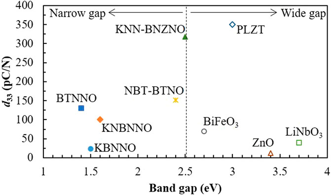
FIGURE 1. Band gaps and d33 values of narrow band gap and wide band gap piezoelectrics discovered to date. KBNNO–(K,Ba) (Nb,Ni)O3-δ; KNBNNO–(K,Na,Ba) (Nb,Ni)O3-δ; KNBNZNO–(K0.48Na0.52)NbO3-(Bi0.5Na0.5) (Zr0.55Ni0.45)O3-δ; NBT-BTNO–(Na0.5Bi0.5)TiO3-Ba(Ti0.5Ni0.5)O3-δ; BTNNO–Ba(Ti,Ni,Nb)O3-δ. Data are extracted from literature (Yue and Yi-jian, 2003; Bavbande et al., 2012; Kumar and Kim, 2012; Mamoun et al., 2013; Bowen et al. 2014; Paillard et al., 2016; Wu et al. (2016); Bai et al., 2017a, Bai et al., 2018a; Durruthy-Rodríguez et al., 2018; Xiao et al. (2019a); Zhong et al. 2019; Lou et al., 2019).
The only strategy that has been preliminarily proven to work on the tuning of band gaps of piezoelectrics with an oxide perovskite structure, is the introduction of Ni2+ ions into the B site associated with oxygen vacancies. Such a strategy was initially studied theoretically via simulations with PbTiO3 as early as 2008 (Bennett et al., 2008; Gou et al., 2011; Qi et al., 2011). According to computed results, the wide band gaps of typical oxide perovskites are due to charge transfer difficulties caused by metal-oxygen bonds, such as the bonds between A site and oxygen and between B site and oxygen. Ni2+-oxygen vacancy combinations may ease the charge transfer from the oxygen 2p states at the valance band maximum to the transition metal d states at the conduction band minimum and thus may be able to reduce the band gap of oxide perovskites. However, Ni2+-doped PbTiO3 has not been validated in experiments because of fabrication difficulties for reasons that are unclear. The author assumes the tolerance factor might have played an important role (Rödel et al., 2009). This doping strategy was finally proved experimentally for the first time in 2013 with another perovskite oxide, KN, rather than PbTiO3 (Grinberg et al., 2013).
The band gap of pure KN has been widely reported to be <3.5–4 eV (Shafir et al., 2020). The first ever experimentally validated narrow band gap piezoelectric material based on an oxide perovskite structure was KBNNO (Grinberg et al., 2013; Bai et al., 2017a). Ni2+-oxygen vacancy combinations were brought into the structure of KN via the doping of Ba(Ni0.5Nb0.5)O3-δ (BNNO) because BNNO is a phase naturally containing oxygen vacancies (therefore KBNNO may also be referred as KN-BNNO). The introduction of the extra element, Ba, on the A site might be detrimental to ferroelectricity as the ionic radius of Ba2+ (1.61 Å in 12-fold coordination) is smaller than that of K+ (1.64 Å in 12-fold coordination) which is likely to lead to a unit cell distortion. On the other hand, Ba2+ also seemed to be able to reduce the sintering difficulty and hygroscopic feature of KN and KNN (Bai et al., 2019b), which is a positive effect.
The firstly reported work of KBNNO managed to reduce the band gap of the parental KN down to 1.4 eV with the composition of KN doped with 10 mol % BNNO, i.e., (K0.9Ba0.1) (Nb0.95Ni0.05)O2.975, where the saturated ferroelectric hysteresis loops could be measured, although at low temperatures (77–170 K) (Grinberg et al., 2013). However, the remanent polarization dropped to negligible levels at room temperature. Following this work, Bai et al. for the first time successfully measured ferroelectricity and thus piezoelectricity (d33 ≈ 23 pC/N) at room temperature for ceramics of KN doped with 10 mol % BNNO with a band gap of about 1.5 eV, through improvement of sample quality (e.g., better densification) (Bai et al., 2017a). These results showed that narrow band gap piezoelectrics with oxide perovskite structures are viable, despite the piezoelectric properties being relatively weak.
It should be noted the Ni doping strategy in KN, as well as in other compositions presented below, is still under debate (Pascual-Gonzalez, 2017; Wu, 2019). This is because although the partial replacement of Ni on the B-site could indeed reduce the band gap, the extent of the reduction has not been agreed in literature. Many factors, including the fabrication process, composition, phase and microstructure, seem to be able to affect the measured band gaps of Ni doped KN and relevant compositions. This issue is subject to further research.
In order to further improve the piezoelectric properties of the narrow band gap KBNNO, Bai et al. replaced the parental KN with KNN and reduced the doping concentration of BNNO (KNBNNO or KNN-BNNO). The ceramics of KNN doped with 2 mol % BNNO exhibited a band gap of 1.6 eV and a d33 of 100 pC/N (Bai et al., 2017b). This is another milestone in the development of narrow band gap piezoelectrics by proving that a small concentration of Ni2+-oxygen vacancy combinations could be enough to significantly reduce the band gap (from >4 eV for KNN), and the d33 value could be retained at the level of the parental KNN (d33 = 90–110 pC/N) (Bai et al., 2017b). The small doping concentration also indicated the effectiveness of the band gap engineering strategy.
Guo et al. further developed the Ni-doped KNN-based compositions with 0.96(K0.48Na0.52)NbO3-0.04(Bi0.5Na0.5) (Zr0.55Ni0.45)O3-δ (0.96–0.04KNBNZNO) of which the d33 reached a relatively high value of 318 pC/N (Zhong et al., 2019), even higher than that of the parental composition KNBNZ and close to that of PLZT. The large d33 value here was attributed to several possible reasons. The parental composition here, KNBNZ, constructed an MPB between two ferroelectric phases, inducing increased domain wall mobility and thus large piezoelectricity (Zheng et al., 2018). Meanwhile, it was claimed that the introduction of Ni2+-oxygen vacancy combinations may help to flatten the free-energy profile by inducing heterogeneous polar regions and additional interfacial energies especially at the MPB and thus enhancing piezoelectricity (Zhong et al., 2019). In addition, in KNBNZNO Ni2+ was added individually without associated Ba2+, which might eliminate the negative effect of Ba2+ on the ferroelectricity and thus piezoelectricity as presented above.
The band gap of 0.96-0.04KNBNZNO could be undoubtedly determined as 2.5 eV (reduced from 3.1 eV of KNBNZ) (Zhong et al., 2019). Nevertheless, gap states at 0.9 and 1.6 eV were also found (Zhong et al., 2019). This is different from the KNN doped with 2 mol % BNNO (0.98KNN-0.02BNNO) where a single band gap without gap states was observed (Bai et al., 2017b). Figure 2 shows the absorption behaviors of 0.98KNN-0.02BNNO and KNBNZNO ceramics samples. In Figure 2A, the absorbance of the 0.98KNN-0.02BNNO presents a smooth curve, implying a single band gap. In Figure 2B, the first absorption edges appeared at about 400 nm, corresponding to their intrinsic band gaps (presented above) caused by band-band transitions from O 2p (or oxygen vacancy) states to Ni 3d states. Additional absorption peaks can be seen at 700 and 1,200 nm, indicating two possible gap states in KNBNZNO. The gap states were proposed to be resulting from the transit of unpaired electrons at Ni 3d states to the conduction band minimum (0.9 eV) and electron transfer from the valence band maximum to the Ni 3d states (1.6 eV). This implies that the local density of states of Ni as well as their interactions with other elements must be different in KNBNNO and KNBNZNO. Such a difference has not been fully understood to date.
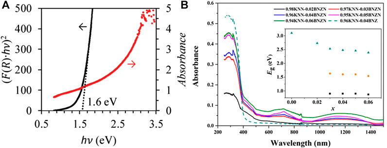
FIGURE 2. Absorbance and band gap determination of (A) 0.98KNN-0.02BNNO and (B) different compositions of KNBNZNO. Eg–band gap; hν–photon energy; R–reflectance. Reproduced with permissions (Bai et al., 2017b; Zhong et al., 2019). Copyrights 2017 and 2019, Wiley.
NBT-BT is another broadly researched piezoelectric composition with a band gap of about 3 eV. Apart from KNBNZNO, Guo et al. also investigated Ni-doped NBT-BT, with the ceramics of composition 0.95(Na0.5Bi0.5)TiO3-0.05Ba(Ti0.5Ni0.5)O3-δ (0.95NBT-0.05BTNO) exhibiting a d33 of 151 pC/N and a band gap of 2.4 eV (Xiao et al., 2019a). Similar to KNBNZNO, the relatively high d33 value (compared to ≈130 pC/N for the parental composition, 0.95(Na0.5Bi0.5)TiO3-0.05BaTiO3) was also believed to be achieved at the MPB with defect-induced local heterogeneous polar regions as presented above. Like KNBNZNO, two other gap stages at 0.9 and 1.4 eV were detected, which was explained using the same mechanism as presented above, i.e., the transition of unpaired electrons at Ni 3d states (Xiao et al., 2019a).
Theoretically, the gap states may act as charge trapping centers tending to degrade the photocurrent, but this is not favored. To address this issue, Guo et al., continued to introduce N into NBT-BTNO (Xiao et al., 2020). The charges associated with N3- and Ni2+ were thought to be balanced by each other, contributing to the removal of gap states, and thus a single gap of 2.1 eV was achieved with the N-doped NBT-BTNO (Xiao et al., 2020). The influence of N in the structure on piezoelectricity is yet to be examined. On the other hand, in order to eliminate the charge trapping effect caused by the oxygen vacancies in the structure, decreasing the ratio between Na+ and Bi3+ ions could balance the chemical valence and hence was able to reduce the concentration of oxygen vacancies while maintaining a high d33 (166 pC/N compared to 151 pC/N for NBT-BTNO with higher oxygen vacancy concentration), as well as supporting a narrow band gap of 2.2 eV (Xiao et al., 2019b).
Although having been proven by KN-, KNN- and NBT-based compositions, the effectiveness of the Ni2+-oxygen vacancy doping strategy for band gap engineering of perovskite oxides was questioned by a BT-based composition. It was found that by doping 1–4 mol % BNNO into BT, the sintered ceramics showed band gaps of 1.4–1.9 eV with d33 values of 70–130 pC/N (Lou et al., 2019). However, the powders made by crushing the sintered ceramics showed the same band gap of 3.1 eV which was identical to that of the undoped BT (Lou et al., 2019). Based on this observation, it was proposed that although the Ni2+-oxygen vacancy combination was able to largely reduce the band gap, the composition containing such a combination was in fact accumulated at grain boundaries and was not diffused into the unit cells of the grains (Lou et al., 2019). To date, the kinetics of Ni2+ ions and oxygen vacancies during the formation of perovskite oxide powders and ceramics have not been clarified.
Organic-inorganic hybrid (or organometal) halide perovskites like MAPbI3, MASnI3, and MAGeI3 (MA = CH3NH3) can possess band gaps of 1.2–1.9 eV and show theoretical d33 values of 27–101 pC/N (Liu et al., 2016). Therefore, in principle they can also be considered as narrow band gap piezoelectrics. However, due to their high leakage currents and structural instability especially when subject to strain, piezoelectric properties agreeing with the theoretical predictions have not been successfully measured in experiments, not to mention practical applications as could be expected for their oxide counterparts presented above. Readers can refer to literature (Kim et al., 2016; Eom et al., 2018; Jella et al., 2018, Jella et al., 2019; Ippili et al., 2019; Shahrokhi et al., 2020) for potential applications (if any) incorporating the piezoelectricity of halide perovskites that could be realized in the future.
Narrow band gap piezoelectrics share the same potential applications employing the photostrictive effect with their wide gap counterparts but will provide additional benefits because of their capability of being driven by visible light with different wavelengths unlike the wide gap materials with violet and UV light as the only options. Although the photocurrents of narrow band gap piezoelectrics are measured to be orders of magnitude smaller than the photovoltaic materials used in solar cells (e.g., Si and organometal halide perovskites), they are in fact already orders of magnitude larger than those of PLZT (Bai et al., 2018b; Xiao et al., 2019a). This gives a hope for narrow band gap piezoelectrics to be qualified as light sensors in addition to conventional kinetic piezoelectric sensors.
Uchino et al. have comprehensively described the potential applications of photostrictive actuators (Poosanaas et al., 2000; Shih et al., 2008). Using the photostrictive effect, photo-acoustic transducers, light-source chasing devices and remotely controllable actuators may be developed. Using KNBNNO, the photostrictive effect could be improved by more than 50% compared to the parental KNN thanks to the reduced band gap and hence promising more effective light absorption (Fu et al., 2020). Therefore, beside photo-actuators, opto-electric dual actuators can also be developed in the future using both visible light and electric field as the double driving forces. This may provide an additional degree of freedom to control the actuation, i.e., in both contacting and contactless modes. One challenge for photo-actuators using the photostrictive effect as the working mechanism is that both the response and decay times are long, meaning a low frequency of operation which significantly limits the feasibility. This issue has to be addressed by, for instance, making thin-film devices and nano-sized domain structures to shorten the response time by orders of magnitude before photostriction can be reliably used in practical devices.
Photostriction utilizes the converse piezoelectric effect for actuation. On the other hand, the direct piezoelectric effect can be used with the photovoltaic effect in narrow band gap piezoelectrics. The most straightforward potential application can be expected as the dual-source sensor, i.e., using the piezoelectric and photovoltaic effects to detect kinetic and optical stimuli, respectively. Since the piezoelectric effect generates an AC output signal and the photovoltaic effect generates a DC output signal, the signals can be distinguished from each other even when being generated at the same time, and thus the dual-source sensing functions can be operated not only individually but also simultaneously. This feature brings a fundamental advancement to the utilization of a single narrow band gap piezoelectric material to realize multiple sensing functions. Bai et al. have reported a single-material optic-kinetic double sensor (and an optic-kinetic-thermal multi-sensor) using KNBNNO (Bai et al., 2020). Figure 3A shows the output profile of the single-material double sensor. It can be seen that, either working individually or simultaneously, the output signals from the piezoelectric and photovoltaic effects excited by external vibration and light, respectively, are well distinguishable and can be used for sensing from the double sources. Alternatively, the light sensing function can be realized via the resistive mode. As shown in Figure 3B, the resistivity of KNBNNO changes significantly with different light wavelengths and intensities (Bai et al., 2018b), offering an operation principle for light sensing.
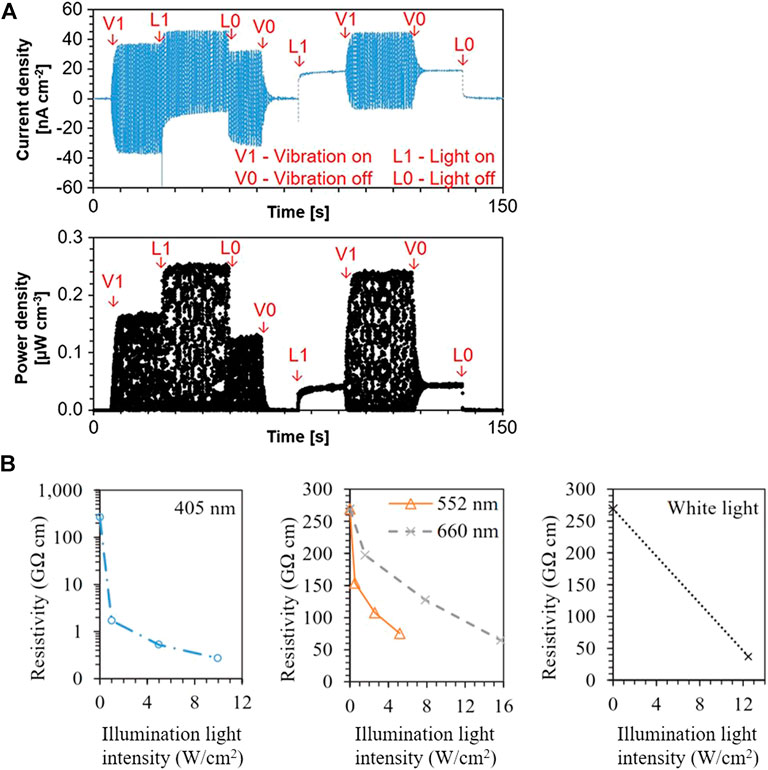
FIGURE 3. (A) Output current and power densities of a single-material, dual-source sensor using KNBNNO from the piezoelectric and photovoltaic effects excited by vibration and light, respectively. (B) Dependence of resistivity on light wavelength and intensity for a KNBNNO ceramic sample. Reproduced with permissions (Bai et al., 2018b; Bai et al., 2020). Copyrights 2018 and 2020, Wiley.
Furthermore, as the piezoelectric effect has been increasingly used for energy harvesting, i.e., converting kinetic energy into electricity thus to power wireless sensors (Bai et al., 2018a), the narrow band gap piezoelectrics can also be used as a double-source energy harvester from both kinetic and light sources. The major benefit here is that, using a single material, one energy source can be harvested to provide power for necessary electronics (e.g., microcontroller, data transmitter, etc.) and the other energy source can be used for sensing (Bai et al., 2019a; Bai et al., 2020). This will enable the design and implementation of truly self-powered sensors. To make this concept a reality, the challenge of developing a material that can simultaneously exhibit excellent piezoelectric and photovoltaic effects which are individually competitive to e.g., the PZT family and Si/organometal halide perovskites, respectively, which has not been achieved to date, must be addressed in the near future.
Pioneer research on band gap engineering of piezoelectrics has mainly focused on Ni-doping in ferroelectric perovskites, as presented in this mini review. This is because Ni is the first non-d0 metal found to work in both theoretical simulation and experimental validation. However, the doping of other non-d0 metals which have similar chemical and physical properties to Ni, including but not limited to Fe, Co, Cr, and Cu, can be modeled in first principle calculations and then trialled in experiments. Solubility and tolerance factor should be considered in the calculations and experiments, which may impose limitations on forming stable perovskite unit cells. To solve this issue, co-doping on the A-sites or B-sites may be employed to balance the tolerance factor using elements with different ionic radii which often appear in perovskites, e.g., K, Na, Ba, Pb, Bi, Sr, Zr, Ti, etc.
In conclusion, having been under development for about 8 years, several material options are already available for piezoelectrics co-exhibiting narrow band gaps and reasonably good piezoelectric properties. Preliminary experiments have been carried out to explore feasible applications of narrow band gap piezoelectrics. However, three major research questions or research tasks need to be rigorously addressed in further developments.
1 New materials with simultaneously excellent piezoelectric and photovoltaic properties are in urgent demand. Excellent piezoelectric properties refer to those competitive when compared to the PZT family (e.g., d33 can reach 600 pC/N, electromechanical coupling factor can reach 0.6 or higher, etc.). Excellent photovoltaic properties mean a large absorption coefficient, large charge carrier diffusion length, weak charge recombination and a long charge carrier lifetime. Boosting the photovoltaic properties is also a major task in the field of photoferroelectrics or ferroelectric photovoltaics, which is shared by the topic of narrow band gap piezoelectrics. Incorporating the guidance provided by first-principle calculations and AI (artificial intelligence) assisted material design methods will stimulate the accomplishment of the mission.
2 Creative designs of devices based on narrow band gap piezoelectrics for novel applications are also needed. The author believes that the cumulative utilization of photovoltaic (or optoelectric) and piezoelectric effects will inspire completely new applications in the future which we cannot currently think of. In a foreseeable future, various self-powered, multi-functional sensors targeting the market of IoT can be designed and fabricated. This should be a perspective that can be reliably expected.
3 As the piezoelectric and photovoltaic signals are generated from the same material, the extraction and separation of signals may require some advanced circuitry designs. Because the piezoelectric response can be derived from various coupling directions (e.g., 33, 31, 15), and the photovoltaic effect is also switchable in photo-ferroelectrics, narrow band gap piezoelectrics have the opportunity to make the best use of these coupling options and thus to build different pairs of electrodes, eventually in order to be able to extract piezoelectric and photovoltaic signals with a great freedom.
Piezoelectric materials have entered new era of having narrow band gaps. The author hopes to inspire both renowned experts in the field and researchers having recently joined the community to think more and put more efforts into the research of narrow band gap piezoelectrics. If ideal materials can be developed in the near future, they will definitely become an influential topic in materials and electronics research as well as in relevant industries.
The author confirms being the sole contributor of this work and has approved it for publication.
This work was financed by the joint funding of the University of Oulu and Academy of Finland profiling action “Ubiquitous wireless sensor systems” (grant number 24302332).
The authors declare that the research was conducted in the absence of any commercial or financial relationships that could be construed as a potential conflict of interest.
Bai, Y., Jantunen, H., and Juuti, J. (2018a). Energy harvesting research: the road from single source to multisource. Adv. Mater. 30, 1707271. doi:10.1002/adma.201707271
Bai, Y., Jantunen, H., and Juuti, J. (2019a). Ferroelectric oxides for solar energy conversion, multi-source energy harvesting/sensing, and opto-ferroelectric applications. ChemSusChem. 12, 2540–2549. doi:10.1002/cssc.201900671
Bai, Y., Palosaari, J., Tofel, P., and Juuti, J. (2020). A single-material multi-source energy harvester, multifunctional sensor, and integrated harvester–sensor system—demonstration of concept. Energy Technol. 8, 2000461. doi:10.1002/ente.202000461
Bai, Y., Siponkoski, T., Peräntie, J., Jantunen, H., and Juuti, J. (2017a). Ferroelectric, pyroelectric, and piezoelectric properties of a photovoltaic perovskite oxide. Appl. Phys. Lett. 110, 063903. doi:10.1063/1.4974735
Bai, Y., Tofel, P., Palosaari, J., Jantunen, H., and Juuti, J. (2017b). A game changer: a multifunctional perovskite exhibiting giant ferroelectricity and narrow bandgap with potential application in a truly monolithic multienergy harvester or sensor. Adv. Mater. 29, 1700767. doi:10.1002/adma.201700767
Bai, Y., Vats, G., Seidel, J., Jantunen, H., and Juuti, J. (2018b). Boosting photovoltaic output of ferroelectric ceramics by optoelectric control of domains. Adv. Mater. 30, e1803821. doi:10.1002/adma.201803821
Bai, Y., Xiang, H., Jantunen, H., and Juuti, J. (2019b). Multi-functional perovskites–an investigation of compositional and processing influence on microstructure, dielectric and ferroelectric properties. Eur. Phys. J. Spec. Top. 228, 1555–1573. doi:10.1140/epjst/e2019-800132-8
Bavbande, D. V., Kumar, R., Bafna, V. H., Mohan, D., and Kothiyal, G. P. (2012). Synthesis and piezoelectric properties of PLZT ceramics. AIP Conf. Proc. 1447, 1341–1342. doi:10.1063/1.4710510
Bennett, J. W., Grinberg, I., and Rappe, A. M. (2008). New highly polar semiconductor ferroelectrics through d8 cation-O vacancy substitution into PbTiO3: a theoretical study. J. Am. Chem. Soc. 130, 17409–17412. doi:10.1021/ja8052249
Bowen, C. R., Kim, H. A., Weaver, P. M., and Dunn, S. (2014). Piezoelectric and ferroelectric materials and structures for energy harvesting applications. Energy Environ. Sci. 7, 25–44. doi:10.1039/C3EE42454E
Brody, P. S. (1983). Optomechanical bimorph actuator. Ferroelectrics 50, 27–32. doi:10.1080/00150198308014428
Damjanovic, D. (1998). Ferroelectric, dielectric and piezoelectric properties of ferroelectric thin films and ceramics. Rep. Prog. Phys. 61, 1267–1324. doi:10.1088/0034-4885/61/9/002
Durruthy-Rodríguez, M. D., Gervacio-Arciniega, J. J., Hernández-García, M., and Yáñez-Limón, J. M. (2018). Photoluminescence characteristics of soft PZT 53/47 ceramic doped at A and/or B sites. J. Adv. Ceram. 7, 109–116. doi:10.1007/s40145-018-0262-8
Eom, J.-H., Choi, H.-J., Pammi, S. V. N., Tran, V.-D., Kim, Y.-J., Kim, H.-J., et al. (2018). Self-powered pressure and light sensitive bimodal sensors based on long-term stable piezo-photoelectric MAPbI3 thin films. J. Mater. Chem. C 6, 2786–2792. doi:10.1039/C8TC00081F
Fu, H., Wang, Y., Guo, H., Lu, Y., Wang, N., Zheng, H., et al. (2020). Boosting the photostriction properties of (K0.5Na0.5)NbO3-based ceramics modulated by introducing Ba(Ni0.5Nb0.5)O3−δ. J. Mater. Chem. C 8, 5904–5912. doi:10.1039/C9TC06824D
Gou, G. Y., Bennett, J. W., Takenaka, H., and Rappe, A. M. (2011). Post density functional theoretical studies of highly polar semiconductive Pb(Ti1−xNix)O3−x solid solutions: effects of cation arrangement on band gap. Phys. Rev. B 83, 205115. doi:10.1103/PhysRevB.83.205115
Grinberg, I., West, D. V., Torres, M., Gou, G., Stein, D. M., Wu, L., et al. (2013). Perovskite oxides for visible-light-absorbing ferroelectric and photovoltaic materials. Nature 503, 509–512. doi:10.1038/nature12622
Ippili, S., Jella, V., Eom, J.-H., Kim, J., Hong, S., Choi, J.-S., et al. (2019). An eco-friendly flexible piezoelectric energy harvester that delivers high output performance is based on lead-free MASnI3 films and MASnI3-PVDF composite films. Nano Energy 57, 911–923. doi:10.1016/j.nanoen.2019.01.005
Jella, V., Ippili, S., Eom, J.-H., Kim, Y.-J., Kim, H.-J., and Yoon, S.-G. (2018). A novel approach to ambient energy (thermoelectric, piezoelectric and solar-TPS) harvesting: realization of a single structured TPS-fusion energy device using MAPbI3. Nano Energy 52, 11–21. doi:10.1016/j.nanoen.2018.07.024
Jella, V., Ippili, S., Eom, J.-H., Pammi, S. V. N., Jung, J.-S., Tran, V.-D., et al. (2019). A comprehensive review of flexible piezoelectric generators based on organic-inorganic metal halide perovskites. Nano Energy 57, 74–93. doi:10.1016/j.nanoen.2018.12.038
Kim, Y.-J., Dang, T.-V., Choi, H.-J., Park, B.-J., Eom, J.-H., Song, H.-A., et al. (2016). Piezoelectric properties of CH3NH3PbI3 perovskite thin films and their applications in piezoelectric generators. J. Mater. Chem. A 4, 756–763. doi:10.1039/C5TA09662F
Kumar, B., and Kim, S.-W. (2012). Energy harvesting based on semiconducting piezoelectric ZnO nanostructures. Nano Energy 1, 342–355. doi:10.1016/j.nanoen.2012.02.001
Kundys, B., Viret, M., Colson, D., and Kundys, D. O. (2010). Light-induced size changes in BiFeO3 crystals. Nat. Mater. 9, 803–805. doi:10.1038/nmat2807
Li, F., Lin, D., Chen, Z., Cheng, Z., Wang, J., Li, C., et al. (2018). Ultrahigh piezoelectricity in ferroelectric ceramics by design. Nat. Mater. 17, 349–354. doi:10.1038/s41563-018-0034-4
Liu, S., Zheng, F., Grinberg, I., and Rappe, A. M. (2016). Photoferroelectric and photopiezoelectric properties of organometal halide perovskites. J. Phys. Chem. Lett. 7, 1460–1465. doi:10.1021/acs.jpclett.6b00527
Lopez-Varo, P., Bertoluzzi, L., Bisquert, J., Alexe, M., Coll, M., Huang, J., et al. (2016). Physical aspects of ferroelectric semiconductors for photovoltaic solar energy conversion. Phys. Rep. 653, 1–40. doi:10.1016/j.physrep.2016.07.006
Lou, Q., Zeng, J., Man, Z., Zheng, L., Park, C., Kassiba, A., et al. (2019). The effect of grain boundary on the visible light absorption of BaTi1−x[Ni1/2Nb1/2]xO3-δ ferroelectric ceramics. J. Am. Ceram. Soc. 102, 7405–7413. doi:10.1111/jace.16643
Mamoun, S., Merad, A. E., and Guilbert, L. (2013). Energy band gap and optical properties of lithium niobate from ab initio calculations. Comput. Mater. Sci. 79, 125–131. doi:10.1016/j.commatsci.2013.06.017
Paillard, C., Bai, X., Infante, I. C., Guennou, M., Geneste, G., Alexe, M., et al. (2016). Photovoltaics with ferroelectrics: current status and beyond. Adv. Mater. 28, 5153–5168. doi:10.1002/adma.201505215
Pascual-Gonzalez, C. (2017). Processing-composition-structure effects on the optical band gap of KNbO3-based ceramics. PhD thesis. Sheffield, United Kingdom: Sheffield Hallam University.
Pimputkar, S., Speck, J. S., DenBaars, S. P., and Nakamura, S. (2009). Prospects for LED lighting. Nat. Photon. 3, 180–182. doi:10.1038/nphoton.2009.32
Polman, A., Knight, M., Garnett, E. C., Ehrler, B., and Sinke, W. C. (2016). Photovoltaic materials: present efficiencies and future challenges. Science 352, aad4424. doi:10.1126/science.aad4424
Poosanaas, P., Tonooka, K., and Uchino, K. (2000). Photostrictive actuators. Mechatronics 10, 467–487. doi:10.1016/S0957-4158(99)00073-2
Qi, T., Grinberg, I., and Rappe, A. M. (2011). Band-gap engineering via local environment in complex oxides. Phys. Rev. B 83, 224108. doi:10.1103/PhysRevB.83.224108
Rödel, J., Jo, W., Seifert, K. T. P., Anton, E.-M., Granzow, T., and Damjanovic, D. (2009). Perspective on the development of lead-free piezoceramics. J. Am. Ceram. Soc. 92, 1153–1177. doi:10.1111/j.1551-2916.2009.03061.x
Shafir, O., Bai, Y., Juuti, J., and Grinberg, I. (2020). Visible-light-absorbing potassium niobate-titanate-molybdate ferroelectrics. Phys. Rev. Appl. 14, 44052. doi:10.1103/PhysRevApplied.14.044052
Shahrokhi, S., Gao, W., Wang, Y., Anandan, P. R., Rahaman, M. Z., Singh, S., et al. (2020). Emergence of ferroelectricity in halide perovskites. Small Methods 4, 2000149. doi:10.1002/smtd.202000149
Shih, H., Rushon, D., Tzou, H., Zheng, W., and Uchino, K. (2008). Photostriction and its use in actuation of flexible structures. J. Eng. Technol. 25, 20–25.
Uchino, K. (2015). Glory of piezoelectric perovskites. Sci. Technol. Adv. Mater. 16, 46001. doi:10.1088/1468-6996/16/4/046001
Uchino, K., Aizawa, M., and Nomura, L. S. (1985). Photostrictive effect in (Pb, La) (Zr, Ti)O3. Ferroelectrics 64, 199–208. doi:10.1080/00150198508018721
Wang, Z. L. (2010). Piezotronic and piezophototronic effects. J. Phys. Chem. Lett. 1, 1388–1393. doi:10.1021/jz100330j
Wang, Z. L., and Wu, W. (2014). Piezotronics and piezo-phototronics: fundamentals and applications. Natl. Sci. Rev. 1, 62–90. doi:10.1093/nsr/nwt002
Wu, J., Fan, Z., Xiao, D., Zhu, J., and Wang, J. (2016). Multiferroic bismuth ferrite-based materials for multifunctional applications: ceramic bulks, thin films and nanostructures. Prog. Mater. Sci. 84, 335–402. doi:10.1016/j.pmatsci.2016.09.001
Wu, L. (2019). Investigation of ferroelectric perovskite oxides for photovoltaic applications. PhD thesis. Pennsylvania (PA): University of Pennsylvania.
Xiao, H., Dong, W., Guo, Y., Wang, Y., Zhong, H., Li, Q., et al. (2019a). Design for highly piezoelectric and visible/near-infrared photoresponsive perovskite oxides. Adv. Mater. 31, 1805802. doi:10.1002/adma.201805802
Xiao, H., Luo, C., Huangfu, G., and Guo, Y. (2020). Boosting the photocatalytic ability of bandgap engineered (Na0.5Bi0.5)TiO3–BaTiO3 by N–Ni codoping. J. Phys. Chem. C 124, 11810–11818. doi:10.1021/acs.jpcc.0c02542
Xiao, H., Wang, Y., Jiao, N., Guo, Y., Dong, W., Zhou, H., et al. (2019b). Understanding the role of oxygen vacancy in visible–near-infrared-light-absorbing ferroelectric perovskite oxides created by off-stoichiometry. Adv. Electron. Mater. 5, 1900407. doi:10.1002/aelm.201900407
Yang, M., Bhatnagar, A., and Alexe, M. (2015). Electronic origin and tailoring of photovoltaic effect in BiFeO3 single crystals. Adv. Electron. Mater. 1, 1500139. doi:10.1002/aelm.201500139
Yue, W., and Yi-jian, J. (2003). Crystal orientation dependence of piezoelectric properties in LiNbO3 and LiTaO3. Opt. Mater. 23, 403–408. doi:10.1016/S0925-3467(02)00328-2
Zheng, T., Wu, J., Xiao, D., and Zhu, J. (2018). Recent development in lead-free perovskite piezoelectric bulk materials. Prog. Mater. Sci. 98, 552–624. doi:10.1016/j.pmatsci.2018.06.002
Keywords: piezoelectric, band gap engineering, absorption, photostriction, multi-functional
Citation: Bai Y (2021) Photoresponsive Piezoelectrics. Front. Mater. 8:636712. doi: 10.3389/fmats.2021.636712
Received: 01 December 2020; Accepted: 26 January 2021;
Published: 26 February 2021.
Edited by:
Dawei Wang, Chinese Academy of Sciences (CAS), ChinaReviewed by:
Antonio Feteira, Sheffield Hallam University, United KingdomCopyright © 2021 Bai. This is an open-access article distributed under the terms of the Creative Commons Attribution License (CC BY). The use, distribution or reproduction in other forums is permitted, provided the original author(s) and the copyright owner(s) are credited and that the original publication in this journal is cited, in accordance with accepted academic practice. No use, distribution or reproduction is permitted which does not comply with these terms.
*Correspondence: Yang Bai, eWFuZy5iYWlAb3VsdS5maQ==
Disclaimer: All claims expressed in this article are solely those of the authors and do not necessarily represent those of their affiliated organizations, or those of the publisher, the editors and the reviewers. Any product that may be evaluated in this article or claim that may be made by its manufacturer is not guaranteed or endorsed by the publisher.
Research integrity at Frontiers
Learn more about the work of our research integrity team to safeguard the quality of each article we publish.