 P. G. Zayas-Bazán1
 K. Gutierrez Z-B1
 O. de Melo1,2,3G. Santana3J. Sastré-Hernández1J. R. Aguilar-Hernández1M. Tufiño-Velázquez1
 G. Contreras-Puente1*
- 1Escuela Superior de Física y Matemáticas, Instituto Politécnico Nacional, Mexico City, Mexico
- 2Physics Faculty, University of Havana, Colina Universitaria, Havana, Cuba
- 3Instituto de Investigación en Materiales, Universidad Nacional Autónoma de México, Cd. Universitaria, Coyoacán, Mexico
In this work, we present the preparation of CdS nanowires (CdS NWs) using the chemical vapor deposition technique and bismuth (Bi) nanoparticles as catalysts. The obtained nanowires were found to be in the hexagonal Greenockite structure according to XRD diffractograms and Raman spectroscopy measurements. Depending on the growth temperature, two kinds of morphologies were observed in SEM images. At low temperature (around 150°C), a high density and homogeneous population of thin and straight nanowires grown through the vapor–liquid–solid mechanism was observed. At higher temperature (around 270°C), thicker bunches of braided nanowires were observed. A quantitative analysis of the temperature-dependent photoluminescence spectra of the CdS NWs was carried out.
Introduction
Semiconductor nanowires have been the subject of intense research because of their novel properties and potential to be incorporated in advanced devices. They exhibit fast 1D growth rate with good crystalline quality, thus leading to advantages in efficiencies and costs (Cui and Lieber, 2001; Huang et al., 2001a; Lieber, 2003; Tang et al., 2011) in opto-electronic devices. CdS nanowires (CdS NWs) used as window material in p-n junction solar cells have the advantage of increasing the effective p-n interface, thus reducing the losses due to photo-carrier recombination and increasing light trapping as well (Liu et al., 2011). Taking this into account, we propose a solar cell with the configuration shown in Figure 1. On the other hand, this nanostructured CdS could be tested as windows material (or even as absorber) in hybrid solar cells, like Quantum Dots Dye Sensitized Solar Cell (QD-DSSC), CdTe, or colloidal CdSeTe. Our argument is supported by the fact that the space in between the nanowires could be embedded by an organic or inorganic photo-absorbent, or micro crystals (Wang et al., 2007; Lee et al., 2009; Grynko et al., 2015). Besides, the incorporation of CdS NWs could have the advantage of providing a direct path for the electrons to the anode, thus decreasing the recombination of photoexcited electrons with the electrolyte (Jasim, 2011; Pan et al., 2018) as a consequence of hopping between nanocrystals as occurs in DSSC cells. Other works carried out in recent years report the use of CdS NWs, combined with other materials such as ZnO, TiO2, and Pt to produce photocatalytic hydrogen under visible light irradiation. In these cases, the CdS NWs showed an efficient charge separation, caused by fast diffusion of the generated photoelectrons, becoming an excellent highly active photocatalyst for the production of hydrogen (Bao et al., 2006; Jang et al., 2008; Barpuzary et al., 2011).
Chemical vapor deposition (CVD) technique, assisted or not by metal catalysts (nanoparticles or very thin layers) is frequently used for preparing CdS NWs (Wang et al., 2002a; Ge and Li, 2004; Kwak et al., 2009). They are obtained by transport of the vapor species to the substrates covered with the catalyst. Different growth mechanisms have been found to be involved in the formation of nanostructures, the most characteristic being the vapor–liquid–solid (VLS) one (Givargizov, 1975; Kolasinski, 2006; Grynko et al., 2013). According to this mechanism, the metal catalyst forms a drop in which vapor species dissolve until oversaturation; then, the excess material precipitates and the nanowire forms with a drop at the tip.
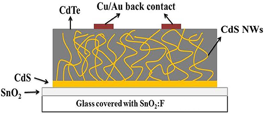
Figure 1. Scheme of a prototype of solar cell using CdS nanowires.
Nanoparticles or very thin layers of gold are more frequently used as catalyst for the growth of nanowires (Huang et al., 2001b; Wang et al., 2002b; Fu et al., 2006; Ma et al., 2007; Zervos and Othonos, 2011). However, Au melting temperature or Au/Cd eutectic (1,064 and 500°C, respectively) are both quite high. In addition, Au has been found to form non-radiative recombination centers in CdS that degrade the optical properties of the nanowires (Schmidt et al., 2009). Bismuth appears to be a suitable catalyst candidate for the preparation of CdS NWs due to its low melting temperature of 271°C and because it forms a eutectic with Cd at 145°C (Keşlioglu et al., 2004). In the last few years, the preparation of nanostructures of several semiconductor materials using Bi as a catalytic metal has been reported (Wang et al., 2006; Ouyang et al., 2007; Sun and Buhro, 2008; Kwak et al., 2009, 2010). In these cases, the nanostructures were obtained using a thin layer of Bi; the solution–liquid–solid mechanism (SLS) has been verified. The use of a relatively large amount of chemicals in SLS growth, with the subsequent generation of by-products during the process, can work against the purity of the prepared material. In contrast, CVD CdS is characterized by a high degree of purity since only CdS vapor species and H2 are present in the growth reactor.
In this work, we used Bi nanoparticles (NPs) to catalyze the growth of CdS NWs. Because of the low temperature of the Cd/Bi eutectic point, we obtained CdS NWs through the VLS mechanism in a CVD configuration at substrate temperatures as low as 145°C. After careful calibration experiments, the flux and the type of gas carrier were found to be determinant for obtaining the growth of nanowires in the VLS regime. Independent of the substrate temperature, two different kinds of morphologies were obtained, and their origin is discussed in relation with the growth parameters.
Experimental
Soda-lime glasses with a fluorine-doped tin oxide layer (TEC15, according to the manufacturer nomenclature, Pilkington, St Helens, United Kingdom) are covered using a triple-magnetron RF-Sputtering (model V3, Intercovamex, Mexico City, Mexico), with layers of sputtered undoped SnO2 (35 nm) and CdS (60 nm) and were used as substrates. In a typical experiment, 10 μl of a suspension composed of 20 g of Bi nanoparticles (NPs) dispersed in 10 ml of methanol was spin-coated onto the substrate at 1,000 rpm for 30 s. Then, the substrate was heated at 70°C for 1 min, allowing the methanol to evaporate. CdS powder (Aldrich 99.999% purity) was located in a graphite boat in the highest temperature region (800°C) of a tubular furnace inside a quartz reactor. Initially, a nitrogen flow of 0.6 L/min was established to remove the air in the reactor. Afterwards, the system was flowed with forming gas (80% Ar/20% H2) at atmospheric pressure at a rate of 0.1 L/min. Downstream, at a coldest region in the reactor (150 or 270°C for samples A and B, respectively), the substrate with the NPs was located (see Figure 2). The growth time was 10 min and, once the process was finished, the system was cooled down under N2 flow.
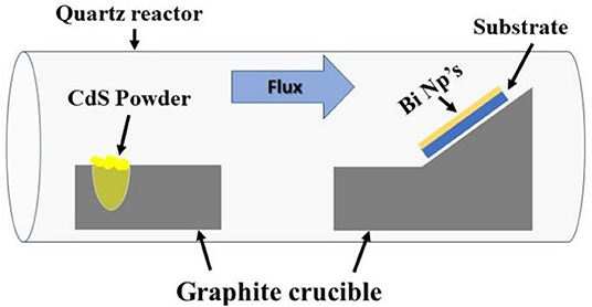
Figure 2. Experimental setup used to grow CdS Nws. The source and substrate are located in two graphite crucibles inside a quartz reactor.
Scanning electron microscopy (SEM) images and energy dispersed spectroscopy (EDS) were obtained with a JSM 7800F JEOL system (Kyoto, Japan) while TEM images were obtained with a JEM-ARM200CF microscope provided with a cold cathode electron gun (Cold Field Emission Gun, CFEG), a spherical aberration corrector CEOS. The x-ray diffractograms were taken with an X'Pert PRO PANalytical diffractometer (Almelo, Netherlands) in fixed grazing incidence angle at room temperature and using Cu-Kα radiation (λ = 1.54056 Å). Raman spectra were measured with a Labram HR800 (Horiba Jobin Yvon, Kyoto, Japan) equipment, with an excitation line of 633 nm with an output power of 10.7 μW and objective magnification of 50×. Photoluminescence (PL) spectra were obtained using a He–Cd laser with an excitation wavelength of 442 nm and output power of 16 mW at room temperature. A double monochromator SPEX-1403 was used to obtain the photoluminescence spectra and the signal was detected using a thermoelectrically cooled photomultiplier RCA-C31034 that is coupled to a photon counter equipment. In other experiments, a 325-nm laser line was used as the excitation source and the sample emission was focused into a photomultiplier tube of an Acton SpectraPro 2500i spectrograph. All the spectra were corrected taking into account the spectral response of the system. No significant differences were found in the spectra that were taken with the two configurations.
Results and Discussion
A secondary electron SEM image of the obtained nanowire forest observed in a typical region of the surface of the sample A is shown in Figure 3A. A high density and a homogeneous population of thin nanowires with straight morphology can be appreciated. In Figure 4, a low-resolution TEM image displays a nanowire around 50 nm thick, with a dark sphere at the tip, which we associate to a bismuth nanoparticle. At the left inset in Figure 4, a high-resolution TEM image allows one to appreciate the crystalline planes in the body of the nanowire. The measurement of the inter-planar distance of these planes indicates that the axial direction of the nanowire coincides with [100] crystalline direction, as frequently observed in CdS NWs (Fu et al., 2006). The nanowires are single crystals as can be observed in the corresponding Fast Fourier Transform in the right inset in Figure 4, which can be indexed as the [001] zone axis; thus, the nanowires grow with the [001] direction normal to the axis of the nanowires. Figure 3B shows an image obtained with the backscattered electron detector, which allows one to better resolve differences in chemical compositions. In this figure, small bright spots with spherical shape distributed throughout the sample surface and located at the tip of the nanowires can be appreciated. These bright spots were identified as Bi according to the EDS spectrum shown in the inset of Figure 3B. This is an indication that the VLS mechanism is responsible for the formation of the nanowires.
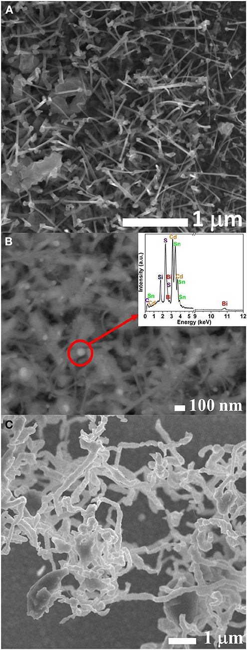
Figure 3. (A) SEM images of the sample A showing a high density of CdS nanowires. (B) Backscattered electron image showing bright spots at the tip of the nanowires. In the inset, an EDS spectrum confirms the presence of Bi in the bright spots. (C) SEM images of the nanowires obtained in sample B with a substrate temperature of 270°C.
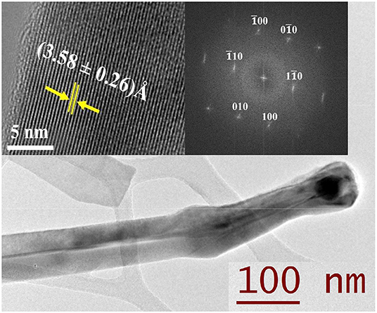
Figure 4. TEM image of the nanowires at low resolution. The left inset shows a high-resolution TEM image in which it is possible to observe the crystalline planes. The Fast Fourier Transform is shown in the right inset, which can be indexed as the [001] zone axis.
The nanowire morphology obtained at a higher substrate temperature of 270°C (sample B), is shown in Figure 3C. In this case, bunches of braided nanowires with diameters ranging between 100 and 300 nm are observed. Also, the nanowire density is smaller than that in sample A.
These morphology differences can be explained considering that, at the higher temperature of the sample B (near to the fusion point of Bi), several Bi nanoparticles can coalesce, forming larger particles and leading to the formation of more than one nanowire in the same catalyst particle.
In the x-ray diffractograms for both samples, shown in Figure 5A, the characteristic reflections of the CdS with Greenockite phase (PDF 41–1,049) are observed. The peaks marked with “+” come from the SnO2 substrate layer with tetragonal phase (PDF 41–1,445), and the peaks around 40° correspond to the planes (104) and (110) of Bi with rhombohedral phase (PDF 44–1,246). The diffractogram of the substrate CdS layer was found to be very weak (see Figure S1 in the supplementary material), which indicates that the main contribution of the diffractograms presented here comes from the CdS NWs.
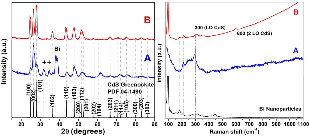
Figure 5. (A) XRD diffractogram for samples A and B showing the characteristic peaks of the CdS with Greenockite phase (the peaks marked with + symbols come from the SnO2 substrate). (B) Raman spectra of nanowires and nanoparticles. The vibrational modes 1LO and 2LO corresponding to CdS with Greenockite phase are observed.
Raman spectra of samples A and B are shown in Figure 5B together with the spectrum of a target fabricated with the Bi nanoparticles. In the spectra, the characteristic emission of the longitudinal optical LO-mode of CdS with Greenockite phase at 300 cm−1 and its 2LO-first harmonic at 600 cm−1 can be appreciated (Nusimovici and Birman, 1967). This result confirms the indication of the x-ray diffraction analysis. The other emissions observed in the Raman spectrum of the nanowires are associated with the Bi nanoparticles: the peaks located around 97 and 185 cm−1 are the first- and second-order Raman scattering mode of bismuth in the rhombohedral structure (Lannin et al., 1975). The increase of the background intensity with increasing energy is associated to the fluorescence in the SnO2 layer of the substrate (similar background was measured in samples with only the SnO2 layer).
Photoluminescence spectra for the samples at low temperature (12–20 K) and room temperature (300 K) are shown in Figure 6. The samples showed an intense and bright luminescence with a narrow peak around 2.5 eV at low temperature, which follows the behavior of near band gap emissions (NBE) (Yang et al., 2012). In fact, deconvolution of these spectra was carried out and the behavior of the intense peak with temperature was found to follow the Varshni equation as it can be observed in the insets, where E0 is the low-temperature band gap and α and β are the Varshni constants (Varshni, 1967) (The complete set of spectra at different temperatures and the deconvolution of the spectra at low temperature can be seen in Figure S2 and Figure S3 in the supplementary material, respectively.). Following previous reports (Thomas and Hopfield, 1962), we assigned this peak to the emission of a bound exciton to a neutral acceptor (I1). The NBE intense peak of sample B is much narrower than that detected for sample A and is slightly shifted. This suggests that the NBE luminescence of sample A is composed of other contributions probably related with defects. This is confirmed by the presence of an intense and wide band centered at around 2.05 eV, known as the “yellow band (YB)” of CdS that has been ascribed to donor–acceptor pairs related to relatively deep centers associated with Cd interstitial (Cdi) or S vacancies (Sv) (Hong et al., 2000; Chandran et al., 2011). The YB has a tail at near 1.9 eV, which can be ascribed to the red band (RB) usually related with surface defects (Shiraki et al., 1974). This combined defect band is more intense for sample A with respect to the NBE emission. At room temperature, spectra are dominated by the so-called “green band (GB)” with a high energy component peaking at near 2.4 eV, which has been related in the literature with a free to bound transition corresponding with the recombination of a free electron with a neutral acceptor (eA0) (Colbow, 1966). The other two peaks present in the GB (resolved only in the spectra of sample B) having an energy separation near the CdS LO phonon (0.037 eV) (Marshall and Mitra, 1964) were considered as the typical phonon replicas of the 2.4-eV transition. According to the above PL analysis, CdS NWs in sample A seem to have a larger amount of defects. This is probably due to the larger surface-to-volume ratio (small diameter) for these nanowires. This can increase surface states as well as Cd vacancies. As a comparison, it is worth noting that the RT luminescence of CdS NWs grown by the SLS mechanism with Bi catalyst is dominated by the yellow band instead (Kwak et al., 2009).
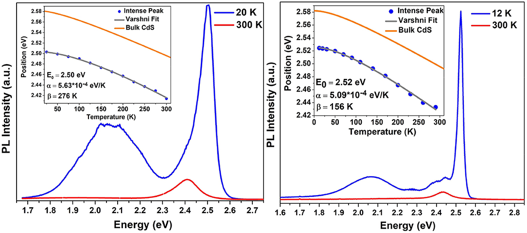
Figure 6. Photoluminescence spectra at low and room temperature of (A) sample A and (B) sample B. In the inset, the fit of the NBE peak to the Varshni equation and the obtained parameters are presented.
It is important to consider that the bands, named YB, eA0, or the unknown surface defect one, have charged state centers whose trapped charges can recombine and give place to the PL emission. The high density of trapped charge centers, originated from the non-crystalline nature of the material, is deleterious for the operation of II–VI solar cells. However, its presence is not completely unavoidable, and defects are always present in the materials, particularly when the surface-to-bulk ratio is high, like in NWs.
Conclusions
The CdS NWs were prepared using the catalytic method with Bi nanoparticles. X-ray diffractograms and Raman spectra verified the presence of CdS hexagonal phase. Depending on the growth temperature, the SEM images revealed two kinds of morphologies. At low temperature, a highly dense and homogeneous population of thin and straight nanowires with diameters <100 nm was obtained. The images obtained by backscattered electrons reveal bright spots with spherical shape at the nanowire tip, indicating a VLS mechanism. At higher temperatures, bunches of braided nanowires with diameters ranging between 100 and 300 nm were observed. These different morphologies can be explained as a consequence of the coalescence of Bi nanoparticles at higher substrate temperature. The study of the PL showed that thin nanowires obtained at low substrate temperature seem to have larger concentration of defects probably because of the large surface-to-volume ratio. CVD CdS NWs prepared with Bi nanoparticles could be used in CdS/CdTe third-generation solar cells with advantages with respect to gold-catalyzed ones. These CdS NWs have good crystalline quality, although defect bands could affect the efficiency of the solar cell. However, we consider it not significant because, at room temperature, this band is almost no appreciable.
Data Availability Statement
The raw data supporting the conclusions of this article will be made available by the authors, without undue reservation, to any qualified researcher on request.
Author Contributions
GC-P and OM contributed to the conception and design of the experiments and also to the analysis of the results. PZ-B and KGZ-B worked on the realization of the experiments, the characterization of the samples, and analysis of the results. GS, JS-H, JA-H, and MT-V worked on the measurements of optical, structural, and morphological properties and also intervened in the analysis of the results. PG and OM wrote the original draft. All authors contributed to manuscript revision, read, and approved the submitted version.
Conflict of Interest
The authors declare that the research was conducted in the absence of any commercial or financial relationships that could be construed as a potential conflict of interest.
Acknowledgments
The authors gratefully acknowledge projects SIP-IPN-20190173, SIP-IPN-20196099, and COFAA-IPN for financial support in the paper publication and CONACyT support. OM thanks the support of UNAM/DGAPA/PREI program 2019. The experimental support of the CNMN-IPN in the realization of the presented works is recognized as well.
Supplementary Material
The Supplementary Material for this article can be found online at: https://www.frontiersin.org/articles/10.3389/fmats.2020.00006/full#supplementary-material
References
Bao, N., Shen, L., Takata, T., Lu, D., and Domen, K. (2006). Highly ordered Pt-loaded CdS nanowire arrays for photocatalytic hydrogen production under visible light. Chem. Lett. 35, 318–319. doi: 10.1246/cl.2006.318
Barpuzary, D., Khan, Z., Vinothkumar, N., De, M., and Qureshi, M. (2011). Hierarchically grown urchinlike CdS@ ZnO and CdS@ Al2O3 heteroarrays for efficient visible-light-driven photocatalytic hydrogen generation. J. Phys. Chem. C 116, 150–156. doi: 10.1021/jp207452c
Chandran, A., Samuel, M.S, Koshy, J., and George, K. C. (2011). Correlated barrier hopping in CdS nanoparticles and nanowires. J. Appl. Phys. 109:084314. doi: 10.1063/1.3569744
Colbow, K. (1966). Free-to-bound and bound-to-bound transitions in CdS. Phys. Rev. 141:742. doi: 10.1103/PhysRev.141.742
Cui, Y., and Lieber, C. M. (2001). Functional nanoscale electronic devices assembled using silicon nanowire building blocks. Science 291, 851–853. doi: 10.1126/science.291.5505.851
Fu, X. L., Li, L. H., and Tang, W. H. (2006). Preparation and characterization of CdS/Si coaxial nanowires. Solid State Commun. 138, 139–142. doi: 10.1016/j.ssc.2006.02.015
Ge, J., and Li, Y. (2004). Selective atmospheric pressure chemical vapor deposition route to CdS arrays, nanowires, and nanocombs. Adv. Funct. Mater. 14, 157–162. doi: 10.1002/adfm.200305051
Givargizov, E. I. (1975). Fundamental aspects of VLS growth. J. Cryst. Growth. 31, 20–30. doi: 10.1016/0022-0248(75)90105-0
Grynko, D. A., Fedoryak, A. N., Dimitriev, O. P., Lin, A., Laghumavarapu, R. B., and Huffaker, D. L. (2013). Growth of CdS nanowire crystals: vapor–liquid–solid versus vapor–solid mechanisms. Surf. Coat. Technol. 230, 234–238. doi: 10.1016/j.surfcoat.2013.06.058
Grynko, D. O., Fedoryak, O. M., Smertenko, P. S., Ogurtsov, N. A., Pud, A. A., Noskov, Y. V., et al. (2015). Multifunctional role of nanostructured CdS interfacial layers in hybrid solar cells. J. Nanosci. Nanotechnol. 15, 752–758. doi: 10.1166/jnn.2015.9171
Hong, K. J., Jeong, T. S., Yoon, C. J., and Shin, Y. J. (2000). The optical properties of CdS crystal grown by the sublimation method. J. Cryst. Growth. 218, 19–26. doi: 10.1016/S0022-0248(00)00491-7
Huang, M. H., Mao, S., Feick, H., Yan, H., Wu, Y., Kind, H., et al. (2001a). Room-temperature ultraviolet nanowire nanolasers. Science 292, 1897–1899. doi: 10.1126/science.1060367
Huang, M. H., Wu, Y., Feick, H., Tran, N., Weber, E., and Yang, P. (2001b). Catalytic growth of zinc oxide nanowires by vapor transport. Adv. Mater. 13, 113–116. doi: 10.1002/1521-4095(200101)13:2<113::AID-ADMA113>3.0.CO;2-H
Jang, J. S., Kim, H. G., Joshi, U. A., Jang, J. W., and Lee, J. S. (2008). Fabrication of CdS nanowires decorated with TiO2 nanoparticles for photocatalytic hydrogen production under visible light irradiation. Int. J. Hydr. Energy 33, 5975–5980. doi: 10.1016/j.ijhydene.2008.07.105
Jasim, K. E. (2011). “Dye sensitized solar cells-working principles, challenges and opportunities,” in The Solar Cells-Dye Sensitized Devices, ed L. A. Kosyachenko (Janeza Trdine; Rijeka: InTech), 172–204.
Keşlioglu, K., Erol, M., Maraşli, N., and Gündüz, M. (2004). Experimental determination of solid–liquid interfacial energy for solid Cd in Bi–Cd liquid solutions. J. Alloy. Comp. 385, 207–213. doi: 10.1016/j.jallcom.2004.05.010
Kolasinski, K. W. (2006). Catalytic growth of nanowires: vapor–liquid–solid, vapor–solid–solid, solution–liquid–solid and solid–liquid–solid growth. Curr. Opin. Solid State Mater. Sci. 10, 182–191. doi: 10.1016/j.cossms.2007.03.002
Kwak, W. C., Han, S. H., Kim, T. G., and Sung, Y. M. (2010). Electrodeposition of Cu (In, Ga) Se2 crystals on high-density CdS nanowire arrays for photovoltaic applications. Cryst. Growth Des. 10, 5297–5301. doi: 10.1021/cg101157a
Kwak, W. C., Kim, T. G., Lee, W., Han, S. H., and Sung, Y. M. (2009). Template-free liquid-phase synthesis of high-density CdS nanowire arrays on conductive glass. J. Phys. Chem. C 113, 1615–1619. doi: 10.1021/jp809365z
Lannin, J. S., Calleja, J. M., and Cardona, M. (1975). Second-order Raman scattering in the group-V b semimetals: Bi, Sb, and As. Phys. Rev. B Condens. Matter. 12:585. doi: 10.1103/PhysRevB.12.585
Lee, J. C., Lee, W., Han, S. H., Kim, T. G., and Sung, Y. M. (2009). Synthesis of hybrid solar cells using CdS nanowire array grown on conductive glass substrates. Electrochem. Commun. 11, 231–234. doi: 10.1016/j.elecom.2008.11.021
Lieber, C. M. (2003). Nanoscale science and technology: building a big future from small things. MRS Bull. 28, 486–491. doi: 10.1557/mrs2003.144
Liu, P., Singh, V. P., Jarro, C. A., and Rajaputra, S. (2011). Cadmium sulfide nanowires for the window semiconductor layer in thin film CdS–CdTe solar cells. Nanotechnology 22:145304. doi: 10.1088/0957-4484/22/14/145304
Ma, R. M., Wei, X. L., Dai, L., Huo, H. B., and Qin, G. G. (2007). Synthesis of CdS nanowire networks and their optical and electrical properties. Nanotechnology 18:205605. doi: 10.1088/0957-4484/18/20/205605
Marshall, R., and Mitra, S. S. (1964). Optically active phonon processes in CdS and ZnS. Phys. Rev. 134:A1019. doi: 10.1103/PhysRev.134.A1019
Nusimovici, M. A., and Birman, J. L. (1967). Lattice dynamics of wurtzite: CdS. Phys. Rev. 156:925. doi: 10.1103/PhysRev.156.925
Ouyang, L., Maher, K. N., Yu, C. L., McCarty, J., and Park, H. (2007). Catalyst-assisted solution– liquid– solid synthesis of CdS/CdSe nanorod heterostructures. J. Am. Chem. Soc. 129, 133–138. doi: 10.1021/ja066243u
Pan, Z., Rao, H., Mora-Seró, I., Bisquert, J., and Zhong, X. (2018). Quantum dot-sensitized solar cells. Chem. Soc. Rev. 47, 7659–7702. doi: 10.1039/C8CS00431E
Schmidt, V., Wittemann, J. V., Senz, S., and Gösele, U. (2009). Silicon nanowires: a review on aspects of their growth and their electrical properties. Adv. Mater. 21, 2681–2702. doi: 10.1002/adma.200803754
Shiraki, Y., Shimada, T., and Komatsubara, K. F. (1974). Optical studies of deep-center luminescence in CdS. J. Appl Phys. 45, 3554–3561. doi: 10.1063/1.1663817
Sun, J., and Buhro, W. E. (2008). The use of single-source precursors for the solution–liquid–solid growth of metal sulfide semiconductor nanowires. Angew. Chem. Int. Ed. 47, 3215–3218. doi: 10.1002/anie.200705142
Tang, J., Huo, Z., Brittman, S., Gao, H., and Yang, P. (2011). Solution-processed core–shell nanowires for efficient photovoltaic cells. Nat. Nanotech. 6:568. doi: 10.1038/nnano.2011.139
Thomas, D. G., and Hopfield, J. J. (1962). Optical properties of bound exciton complexes in cadmium sulfide. Phys. Rev. 128:2135. doi: 10.1103/PhysRev.128.2135
Varshni, Y. P. (1967). Temperature dependence of the energy gap in semiconductors. Phys. A 34, 149–154. doi: 10.1016/0031-8914(67)90062-6
Wang, F., Dong, A., Sun, J., Tang, R., Yu, H., and Buhro, W. E. (2006). Solution– liquid– solid growth of semiconductor nanowires. Inorg. Chem. 45, 7511–7521. doi: 10.1021/ic060498r
Wang, L., Liu, Y., Jiang, X., Qin, D., and Cao, Y. (2007). Enhancement of photovoltaic characteristics using a suitable solvent in hybrid polymer/multiarmed CdS nanorods solar cells. J. Phys. Chem. C 111, 9538–9542. doi: 10.1021/jp0715777
Wang, Y., Meng, G., Zhang, L., Liang, C., and Zhang, J. (2002a). Catalytic growth of large-scale single-crystal CdS nanowires by physical evaporation and their photoluminescence. Chem. Mater. 14, 1773–1777. doi: 10.1021/cm0115564
Wang, Y., Zhang, L., Liang, C., Wang, G., and Peng, X. (2002b). Catalytic growth and photoluminescence properties of semiconductor single-crystal ZnS nanowires. Chem. Phys. Lett. 357, 314–318. doi: 10.1016/S0009-2614(02)00530-4
Yang, Z. X., Zhong, W., Zhang, P., Xu, M. H., Deng, Y., Au, C. T., et al. (2012). Controllable synthesis, characterization and photoluminescence properties of morphology-tunable CdS nanomaterials generated in thermal evaporation processes. Appl. Surf. Sci. 258, 7343–7347. doi: 10.1016/j.apsusc.2012.04.010
Keywords: solar cells, semiconductors, nanowires, photoluminescence, catalytic method
Citation: Zayas-Bazán PG, Gutierrez Z-B K, de Melo O, Santana G, Sastré-Hernández J, Aguilar-Hernández JR, Tufiño-Velázquez M and Contreras-Puente G (2020) Bi Catalyzed CdS Nanowires With Temperature-Dependent Morphologies for Potential Applications in Solar Cells. Front. Mater. 7:6. doi: 10.3389/fmats.2020.00006
Received: 17 November 2019; Accepted: 08 January 2020;
Published: 20 February 2020.
Edited by:
Federico Cesano, University of Turin, ItalyReviewed by:
Oleg Dimitriev, National Academy of Sciences of Ukraine (NAN Ukraine), UkraineAminur Rashid Chowdhury, University of Texas at Austin, United States
Copyright © 2020 Zayas-Bazán, Gutierrez Z-B, de Melo, Santana, Sastré-Hernández, Aguilar-Hernández, Tufiño-Velázquez and Contreras-Puente. This is an open-access article distributed under the terms of the Creative Commons Attribution License (CC BY). The use, distribution or reproduction in other forums is permitted, provided the original author(s) and the copyright owner(s) are credited and that the original publication in this journal is cited, in accordance with accepted academic practice. No use, distribution or reproduction is permitted which does not comply with these terms.
*Correspondence: G. Contreras-Puente, Z3NjcDE5NTNAaG90bWFpbC5jb20=