 Jiahuan Feng1,2†
 Dongwei Sun1,2†Sijiong Mei1,2Wuxing Shi1,2
 Fei Mei1,2*
 Yuanming Zhou1,2*Jinxia Xu1,2Yan Jiang1,2Linzhang Wu2
- 1Hubei Key Laboratory for High-efficiency Utilization of Solar Energy and Operation Control of Energy Storage System, Hubei University of Technology, Wuhan, China
- 2School of Electrical and Electronic Engineering, Hubei University of Technology, Wuhan, China
Organic light-emitting diodes (OLEDs) have drawn a great deal of attention due to their broad applications in lighting and displaying. With the development of nanotechnology, surface plasmas have been widely used in photonics, microscopes, solar cells and biosensors. In this paper, by inserting graphene oxide (GO), Au nanoparticles (Au NPs) and GO/Au NP composite structures between the hole transport layer (NPB) and indium tin oxide (ITO) anode, respectively, the electroluminescent performance of Alq3-based OLEDs was significantly enhanced. Compared to the reference devices, the devices with the composite inserting layer containing 10% GO/Au NP doping have the best electroluminescent performance, which improved 47.9% in maximum luminance, 49.2% in maximum current efficiency and 45.3% in maximum external quantum efficiency (EQE). Such substantial enhancement of photoelectric performance can be attributed to the combined effects of LSPR coupling and the better hole transport property by introducing Au NPs and a graphene oxide-doped layer.
Introduction
Organic light-emitting diodes (OLEDs) have drawn a great deal of attention due to their broad applications in lighting and displaying because they are simple to produce, lightweight, and flexible (Park et al., 2017). The improved efficiency and enhanced device stability are important for their commercialization (Coehoorn et al., 2015; Zhang et al., 2015b) Tremendous effort has been made by many researchers to enhance electroluminescent performance of OLEDs in different ways (Jesuraj et al., 2017). These efforts include heightening the internal quantum efficiency of organic materials (Adachi et al., 2001; Xiao et al., 2009), improving the out-coupling efficiency of the device with an array of lenses (Sun and Forrest, 2008; Han et al., 2018), metal nanoparticles (NPs) (Chen et al., 2017; Zhang et al., 2017), and reasonable nanostructures (Riedel et al., 2010; Chen et al., 2015).
Carbon-based 2-dimensional (2-D) materials such as graphene and graphene oxide (GO) have been widely used in optoelectronic devices due to their unique physical and electronic properties (Wu et al., 2013, 2014b; Basu et al., 2014; Kim et al., 2014; Yeo et al., 2015). Graphene and graphene oxide have great potential for large-area electronics because of their large surface area, high intrinsic mobility, high optical transmittance, etc (Gómez-Navarro et al., 2007; Zhu et al., 2010; Chen et al., 2011; Chabot et al., 2014; Naumov et al., 2016; Jesuraj et al., 2017). The existence of oxygen functional groups on the GO structure makes it dispersible in many solvents and enables its utilization in solution-processable devices (Yun et al., 2011; Shi et al., 2013; Liang et al., 2014; Lee et al., 2015, 2016).
Another effective method, namely the use of plasmonic metallic nanoparticles, has also been used to improve the electroluminescent properties of OLEDs (Choi et al., 2013; Wu et al., 2014a, 2018; Zhang et al., 2015a, 2017; Cho et al., 2016; Balakrishnan and Kamat, 2017). One of the most important properties of plasmonic metallic nanoparticles is surface plasmon resonance (SPR), which is the strong interaction between plasmonic metallic nanoparticles and resonant photons. SPR could promote light emission effectively through an enhanced spontaneous emission rate and thus improve the performance of OLEDs (Xiao et al., 2012; Xu et al., 2017). Furthermore, the light scattering caused by the plasmonic metallic nanoparticles can help extract photons trapped within the substrate or waveguide modes, which increases light extraction efficiency (Chen et al., 2017). The prerequisite to strengthening the coupling effect between metallic nanoparticles and resonant photons is the overlapping between the photoluminescence (PL) spectrum emission layer and the absorption spectrum of metallic nanoparticles, which can be modified by the morphology of the metallic nanoparticles we selected.
As presented in the literature, the electroluminescent performance of OLEDs has been improved by introducing a 2D material between the anode and the hole transport layer (HTL) or utilizing the surface plasmon resonance (SPR) of metallic nanoparticles (MNPs) individually. However, the combination of these two effects has rarely been reported in the research field of OLEDs. In this work, a composite structure comprising Au NPs embedded in GO was introduced as a hole injection layer to take advantage of 2D materials and the plasma effect, which enhance the electroluminescence performance of OLEDs. The volume ratio of Au NPs and the concentration of GO were changed to investigate the optical and electrical properties of the OLED devices. The optimal values of the volume ratio of Au NPs and the GO concentration were found to be 10% and 0.25 mg/ml, respectively. Correspondingly, the OLEDs with GO/Au NPs prepared under these conditions also have the best performance. Compared with the reference devices without Au NPs and GO, the optimal plasmonic OLEDs exhibit better performance in terms of luminance, current efficiency, and EQE. These results suggest that the plasmonic OLEDs have great potential for enhanced performance by introducing Au NPs and GO.
The Experiment
Materials Used
All solvents and reagents were used as received unless otherwise stated. Tetrachloroauratetrihydrate (HAuCl4·3H2O, 99.99%), Trisodium citrate dihydrate (Na3C6H5O7·2H2O, 99.0%) and n-butylamine (C4H11N, 99.0%) were purchased from Shanghai Chemical Reagent Co, Ltd (China). N, N'-Bis (naphthalen-1-yl)-N, N'-bis (diphenyl) benzidine (NPB, 99.5%) and Tris-(8-Hydroxyquinolinato) aluminum (Alq3, 99.5%) were purchased from Jilin Optical and Electronic Materials Co, LTD (China). Lithium Fluoride (LiF, 99.995%) and Aluminum slug (Al, 99.999%) were purchased from Sigma Aldrich and Alfa Aesar, respectively.
Synthesis of Graphene Oxide and Gold Nanoparticles
First, the GO solution was prepared from natural graphite powder by a modified Hummers method. Then, the obtained GO solution was purified through centrifugation (12,000 rpm for 60 min) and washed with deionized water several times until the GO solution was neutral, with a pH value of 7. Through these steps, we finally got the GO aqueous solution with a concentration of 1 mg/ml. Before being used in the fabrication of OLEDs, the GO solution would be stirred through ultrasonication for more than 1 h.
Au NPs with 20 nm diameter were synthesized according to Frens method. The synthesis procedure of Au NPs is based on the HAuCl4 solution and trisodium citrate dihydrate as a reducing agent. Briefly, Au NPs 20 nm in diameter were prepared by adding aqueous HAuCl4 (0.5 ml, 0.05 M) into deionized water (19.5 ml) in a glass tube, and then the obtained solution was brought to a boil while being vigorously stirred. Then, 1.8 ml 0.05 g/ml aqueous trisodium citrate dihydrate was added to the solution. The reaction solution was kept at a boil for 10 min until the solution's color was wine red, indicating that the Au NPs with desired size had been synthesized.
The synthesis process of GO/Au NPs composites was followed by an earlier reported procedure (Fu et al., 2016). 0.25 ml n-butylamine was added to the obtained GO (5 ml 1.0 mg/ml) and then the mixed solution was stirred for 45 min, forming a uniform GO colloid. Then, 5 ml of synthesized solution containing Au NPs was added to the GO colloid. Subsequently, the mixture was heated to 80°C with magnetic stirring and aged at the same temperature overnight. The GO/Au NPs were washed several times and re-dispersed in 5 ml of deionized water before use.
OLED Fabrication
The OLEDs were fabricated on the precleaned patterned ITO glass substrates, whose sheet resistance was ~15 Ω/m2. The ITO substrates were ultrasonically cleaned with acetone, ethanol and deionized water in sequence for 10 min respectively, and then treated with oxygen plasma for 10 min to increase the work function. After these steps, different hole injection layers (HILs), such as GO, Au NPs, and GO/Au NPs, were spin-coated on ITO substrates at 6,000 rmp for 45 s and then annealed at 80°C for 10 min. The typical OLED structure consists of a HIL (GO, Au NPs, or GO/Au NPs composite), a 30 nm NPB as HTL, a 30 nm Alq3 as an emitting layer (EML), a 30 nm Alq3 as an electron transport layer (ETL), a 0.5 nm LiF as an electron inject layer (EIL) and 100 nm Al as a cathode deposited through a special mask, which defines the active area of all these devices to be 0.1 cm2. Four identical devices on each substrate were encapsulated with a glass lid in a N2-filled glove box and then characterized at room temperature.
Characterization
The current density-voltage (J-V) characteristics of the devices were tested using a Keithley 2400 source measure unit, and the EL spectra of the OLEDs were recorded using an Ocean Optics fiber-optic spectrometer. The luminance of the devices was measured by a Keithley 2000 multimeter coupled with a calibrated silicon photodetector (1 cm in diameter), which was put directly onto the surface of an individual device, ensuring that all photons emitted from the glass side were captured. In this procedure, the operating current density is set to be 50 mA/cm2.
The photoluminescence (PL) absorption spectra were measured by a HITACHI F-4600 luminescence spectrometer with an excitation wavelength of 430 nm, and the UV-vis spectra were monitored with a HITACHI U-3900 ultraviolet/visible spectrophotometer. The surface morphology was conducted via scanning electron microscopy (SEM, FEI Sirion FEG). Transmission electron microscopy (TEM, FEI TECNAI G2 20) was used to characterize the topography of Au NPs. The finite-difference timed-domain (FDTD) simulations have been performed to reveal the Au NP-induced plasmon modes.
Results and Discussion
The typical device configuration consists of spin-coated layers of the GO/Au NPs on the surface of the ITO anode and evaporated layers of NPB, Alq3 and LiF/Al, as shown in the schematic diagram in Figure 1A. GO/Au NPs were capped by NPB via spin-coating its aqueous solution on the ITO anode. Figure 1B shows the optical properties of the Au NPs and the evaporated Alq3 film. The TEM image indicates that the Au NPs are spherical in shape and the average diameter is nearly 20 nm. The Au NPs display a typical absorption peak of 524 nm, which is seen in the UV-vis absorption spectrum, while the PL spectrum of the Alq3 film has a peak position around 520 nm. It is evident that the absorption peak of the Au NPs matches the PL peak of the Alq3 films. The overlap of these two spectra provides the possibility for resonance between radiated light generated in the Alq3 emitter and localized SPR excited by the Au NPs, which is expected to result further in effective energy transfer and, correspondingly, enhanced emission intensity (Zhang et al., 2017).
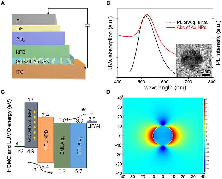
Figure 1. (A) The device structure of the OLEDs by inserting GO/Au NPs between the ITO anode and NPB hole transport layer. (B) The absorption spectrum of Au NP solution and the PL spectrum of Alq3 film on ITO glass. The inset shows the TEM image of the Au NPs. (C) The energy level diagram of the OLEDs. (D) FDTD stimulation of the electromagnetic field distribution around Au NPs with the diameter of 20 nm.
The energy level values in Figure 1C were taken from Ref (Liu et al., 2017) and (Li et al., 2017). It can be seen that the injection of holes from ITO into the Alq3 layer was partly prohibited due to the large energy barrier of ~0.9–1.0 eV, while electrons can be easily injected into Alq3 from LiF/Al. The ITO glass was modified with GO—a material with a high work function (WF)—in order to enhance the hole injection efficiency, finally achieving more balanced hole and electron transport. Figure 1D shows the FDTD stimulation of the electromagnetic field distribution around Au NPs with a diameter of 20 nm, which indicates that the effective range of LSPR is ~10 nm. According to our device structure, the exciton recombination zone would be very close to the NPB/Alq3 interface, which can fall into the electromagnetic fields of Au NPs.
In order to define the effect of Au NPs and GO/Au NP composites on the surface morphology of the NPB film, we studied the SEM images of the NPB films, which are located on the Au NPs and GO/Au NPs composite, respectively. The SEM images showed that the NPB films' morphology changes with Au NPs and GO/Au NPs in Figures 2A,B, respectively. Several Au NPs seen as white spots are distributed randomly in the dense and uniform background, which is the typical image the NPB film fabricated by thermal evaporation. It was expected that introducing GO and Au NPs would not cause notable morphology changes to the NPB films.
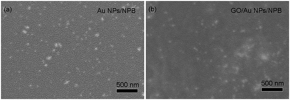
Figure 2. (A) The SEM image of NPB film with Au NPs, in which the volume ratio of Au NPs is 10%. (B) The SEM image of NPB film with GO/Au NPs, in which the volume ratio of GO/Au NPs is 10%.
The J-L-V characteristics of the OLEDs with different volume ratios of Au NPs are illustrated in Figure 3. According to the J-V curves in Figure 3A, on increasing the volume ratio of Au NPs, the current density of the OLED devices decreases at the same bias voltage. In contrast to the trend of J-V characteristics, two distinct evolutions of the maximum luminance were observed in the L-J curves. As the Au NPs' volume ratio increase from 0 to 10%, the maximum luminance increases from 2,380 cd/m2 to 3,050 cd/m2, which is 28.2% higher than that of the control OLEDs. However, when the Au NPs' volume ratio is higher than 10%, the maximum luminance decreases continuously with the Au NPs' volume ratio. The current efficiency and EQE characteristics of the OLEDs are shown in Figures 3C,D, respectively. Compared to the maximum current efficiency and EQE of OLEDs without Au NPs, significant enhancements of 28.2 and 26.4% were obtained in the device with 10% Au NPs, which is very similar to the trend of L-J characteristics. A further increase of the volume ratio of Au NPs leads to a decrease of the current efficiency and EQE.
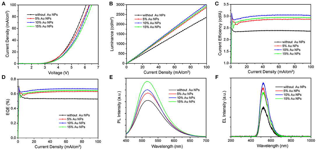
Figure 3. Characteristics of OLEDs with only Au NPs. (A) The J-V characteristics, (B) L-J characteristics, (C) current efficiency, (D) EQE vs. current density characteristics of OLEDs with different volume ratios of Au NPs, (E) PL spectra of Alq3 film and (F) EL spectra of OLEDs with different volume ratios of Au NPs operated at 50 mA/cm2.
As shown in Figure 3E, the PL intensity continues to increase when the Au NPs' doping rate increased from 0 to 15%, suggesting that the SPR effects were also enhanced with larger concentrations of Au NPs. However, the EL performance of the OLEDs, presented in Figure 3F, started to decrease while the Au NPs' volume ratios >10%, similar to the trend for maximum luminance. This can be caused by the competition between two effects, explained as follows: On the one hand, emission strength can be enhanced by the SPR effect caused by the Au NPs. On the other hand, the introduction of Au NPs with higher concentrations may destroy the flat film morphology, resulting in a slow decrease of the current density and poor electroluminescent performance of OLEDs (Chen et al., 2017). All the devices with Au NPs exhibit EL peaks around 520 nm, which is consistent with the PL spectra of the Alq3 films.
The characteristics of the devices with GO interlayers are shown in Figure 4. In this work, GO with three low concentrations (0.25, 0.5, and 0.75 mg/ml) was investigated as a hole injection layer in OLEDs. Meanwhile, the transmittances of ITO and ITO/GO substrates are near-identical, which cannot impede the light emission of OLEDs. The devices with GO interlayers show better performance than the control device without GO in terms of turn-on voltage, luminance, current efficiency, and EQE. For example, the use of 0.5 mg/ml GO leads to a decline of the turn-on voltage from 3.2 to 3.0 V, an improvement of EQE from 0.53 to 0.62% and a significant enhancement of more than 16% in the maximum luminance.
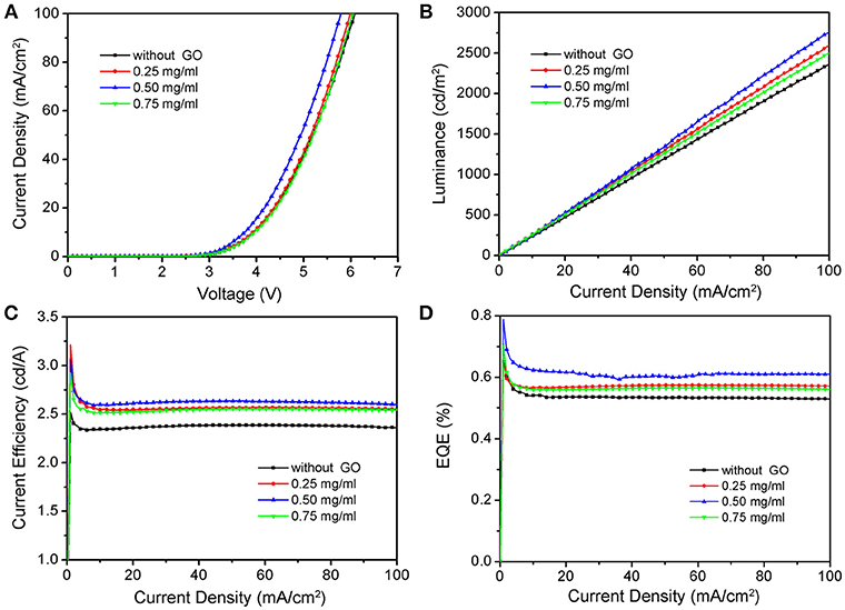
Figure 4. Characteristics of OLEDs with only GO. (A) The J-V characteristics, (B) L-J characteristics, (C) current efficiency, and (D) EQE vs. current density characteristics of OLEDs with different concentrations of GO.
The improvements in device performance can be attributed to the functionality of the GO interlayer. Because all the devices have the same structure on the cathode side, we deduce that the hole injection is improved by the GO interlayer. According to the proposed energy level diagram shown in Figure 1C, the large band gap of GO hinders the transport of electrons from the Al cathode to the ITO, acting as an effective electron blocking layer, which will improve electron-hole recombination in the active layer. Furthermore, the insertion of GO with an improved effective work function (WF) can induce an interface energy step between ITO and Alq3, leading to a reduced energy barrier and an improvement of hole injection efficiency with a concomitant increase in luminance.
In order to obtain the OLEDs with better performance, we also prepared a series of GO/Au NP composites, which were utilized as the hole injection layers for OLEDs. The properties of these devices were presented through the J-L-V characteristics in Figure 5. A substantial enhancement of electroluminescent performance was observed in the OLEDs with GO/Au NP composite structures and the optimal volume ratio was found to be 10%. For the optimal OLEDs, the maximum luminance is ~3,520 cd/m2, which was 47.9% higher than that of the reference device without GO/Au NP composites. Very similar to the trend of J-L characteristics, the maximum current efficiency and EQE first increase with the volume ratio of GO/Au NPs, increasing from 0 to 10% and then decreasing with a further increase of the volume ratio. Additionally, both the maximum current efficiency of ~3.55 cd/A and the maximum EQE of ~0.77% were achieved for the devices with 10% GO/Au NPs, which show substantial enhancements of 49.2 and 45.3%, respectively. On increasing the volume ratio of GO/Au NPs to 15% or decreasing to 0, both current efficiency and EQE decrease. The PL and EL spectra shown in Figures 5E,F are similar to those in Figure 3. Furthermore, it is noted that the increase of both PL and EL intensity is more evident after the insertion of GO. As explained above in Figure 3, despite the enhanced SPR effect, the excessive Au NPs may also cause serious morphological destruction of NPB film, which may take place in the devices with GO/Au NPs, also leading to the slight decrease of the current density.
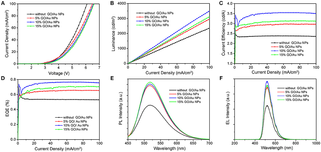
Figure 5. Characteristics of OLEDs with GO/Au NPs. (A) The J-V characteristics, (B) L-J characteristics, (C) current efficiency, (D) EQE vs. current density characteristics of OLEDs with different volume ratios of GO/Au NPs and (E) PL spectra of Alq3 film and (F) EL spectra of OLEDs with different volume ratios of GO/Au NPs operated at 50 mA/cm2.
It is reasonable to conclude that some effects, especially the LSPR coupling at the NPB/Alq3 interface by introducing Au NPs and the improved hole injection by the GO interlayer, have taken place at the ITO/GO/Au NP/NPB interfaces, and help to improve the efficiency of Alq3 OLEDs. First, the resonance between radiated light generated in the Alq3 emitter and localized SPR excited by the Au NPs can lead to an effective energy transfer and, correspondingly, to enhanced emission intensity. Furthermore, GO can optimize the energy level structure of the device and balance electron and hole injection by blocking the flow of electrons from the emissive layer to the ITO and increasing the efficiency of the hole injection, thus further enhancing device performance of OLEDs (Silva et al., 2013).
Conclusions
In summary, we have demonstrated the enhanced luminescence of Alq3 OLEDs with Au NPs, GO and GO/Au NPs interlayer. Compared to the reference devices without GO or Au NPs, the OLEDs with GO/Au NPs exhibit the best performance, with a 47.9% enhancement in maximum luminance, a 49.2% enhancement in maximum current efficiency, and a 45.3% enhancement in EQE. These results can be explained by the SPR coupling between Au NPs and Alq3 excitons as well as the optimized band arrangement by inserting the GO interlayer. As discussed, SPR can facilitate effective energy transfer while the insertion of GO can create more balanced hole and electron transport, with both improving LED performance through enhanced radiative recombination rate. Our results illustrate that the combination between plasmonic Au NPs and GO is effective and has great potential in developing high-efficiency OLEDs, which provides a new way for improving OLED performance.
Author Contributions
All authors listed have made a substantial, direct and intellectual contribution to the work, and approved it for publication.
Conflict of Interest Statement
The authors declare that the research was conducted in the absence of any commercial or financial relationships that could be construed as a potential conflict of interest.
Acknowledgments
This work was supported by the Foundation of Hubei Provincial Science and Technology Department (Grant No. 2016BKJ005), the Leading Plan of Green Industry of Hubei University of Technology (Grant No. YXQN2016003), the International Science and Technology Cooperation Program of China (Grant No. 2016YFE0124300), the Open Foundation of Hubei Key Laboratory for High-efficiency Utilization of Solar Energy and Operation Control of Energy Storage System (Grant Nos. HBSEES201801, HBSEES201705), and the National Natural Science Foundation of China (Grant Nos. 51602099, 51371079, 11304092, and 11375134).
References
Adachi, C., Baldo, M. A., Thompson, M. E., and Forrest, S. R. (2001). Nearly 100% internal phosphorescence efficiency in an organic light emitting device. J. Appl. Phys. 90:5048. doi: 10.1063/1.1409582
Balakrishnan, S. K., and Kamat, P. V. (2017). Au-CsPbBr3 hybrid architecture. anchoring gold nanoparticles on cubic perovskite nanocrystals. ACS Energy Lett. 2, 88–93. doi: 10.1021/acsenergylett.6b00592
Basu, S., Lee, M. C., and Wang, Y. H. (2014). Graphene-based electrodes for enhanced organic thin film transistors based on pentacene. Phys. Chem. Chem. Phys. 16, 16701–16710. doi: 10.1039/C3CP55440F
Chabot, V., Higgins, D., Yu, A., Xiao, X., Chen, Z., and Zhang, J. (2014). A review of graphene and graphene oxide sponge: material synthesis and applications to energy and the environment. Energ. Environ. Sci. 7, 1564–1596. doi: 10.1039/C3EE43385D
Chen, C. Y., Lee, W. K., Chen, Y. J., Lu, C. Y., Lin, H. Y., and Wu, C. C. (2015). Enhancing optical out-coupling of organic light-emitting devices with Nanostructured composite electrodes consisting of indium tin oxide nanomesh and conducting polymer. Adv. Mater. 27, 4883–4888. doi: 10.1002/adma.201502516
Chen, P., Xiong, Z., Wu, X., Shao, M., Meng, Y., Xiong, Z. H., et al. (2017). Nearly 100% efficiency enhancement of CH3NH3PbBr3 perovskite light-emitting diodes by utilizing plasmonic Au nanoparticles. J. Phys. Chem. Lett. 8, 3961–3969. doi: 10.1021/acs.jpclett.7b01562
Chen, X., Wu, G., Chen, J., Chen, X., Xie, Z., and Wang, X. (2011). Synthesis of “clean” and well-dispersive Pd nanoparticles with excellent electrocatalytic property on graphene oxide. J. Am. Chem. Soc. 133, 3693–3695. doi: 10.1021/ja110313d
Cho, C., Kang, H., Baek, S. W., Kim, T., Lee, C., Kim, B. J., et al. (2016). Improved internal quantum efficiency and light-extraction efficiency of organic light-emitting diodes via synergistic doping with Au and Ag nanoparticles. ACS Appl. Mater. Interfaces 8, 27911–27919. doi: 10.1021/acsami.6b07666
Choi, H., Ko, S. J., Choi, Y., Joo, P., Kim, T., Lee, B. R., et al. (2013). Versatile surface plasmon resonance of carbon-dot-supported silver nanoparticles in polymer optoelectronic devices. Nat. Photon. 7, 732–738. doi: 10.1038/NPHOTON.2013.181
Coehoorn, R., Eersel, H. V., Bobbert, P., and Janssen, R. (2015). Kinetic monte carlo study of the sensitivity of OLED efficiency and lifetime to materials parameters. Adv. Funct. Mater. 25, 2024–2037. doi: 10.1002/adfm.201402532
Fu, X., Kuang, P., Wang, S., Zhang, G., and Yin, H. (2016). Controllable synthesis of graphene oxide-silver (gold) nanocomposites and their size-dependencies. RSC Adv. 6, 70468–70473. doi: 10.1039/C6RA11291A
Gómez-Navarro, C., Weitz, R. T., Bittner, A. M., Scolari, M., Mews, A., Burghard, M., et al. (2007). Electronic transport properties of individual chemically reduced graphene oxide sheets. Nano Lett. 7, 3499–3503. doi: 10.1021/nl072090c
Han, K. H., Park, Y. S., Cho, D. H., Han, Y., Lee, J., Yu, B., et al. (2018). Optical analysis of power distribution in top-emitting organic light emitting diodes integrated with nanolens array using finite difference time domain. ACS Appl. Mater. Interfaces. 10, 18942–18947. doi: 10.1021/acsami.8b02631
Jesuraj, J. J., Parameshwari, R., Kanthasamy, K., Koch, J., Pfnür, H., and Jeganathan, K. (2017). Hole injection enhancement in organic light emitting devices using plasma treated graphene oxide. Appl. Surf. Sci. 397, 144–151. doi: 10.1016/j.apsusc.2016.11.110
Kim, J. H., Seo, J., Kwon, D. G., Hong, J. A., Hwang, J., Choi, H. K., et al. (2014). Carrier injection efficiencies and energy level alignments of multilayer graphene anodes for organic light emitting diodes with different hole injection layers. Carbon 79, 636–630. doi: 10.1016/j.carbon.2014.08.024
Lee, C. Y., Le, Q. V., Kim, C., and Kim, S. Y. (2015). Use of silane-functionalized graphene oxide in organic photovoltaic cells and organic light-emitting diodes. Phys. Chem. Chem. Phys. 17:9369. doi: 10.1039/C5CP00507H
Lee, D. Y., Na, S. I., and Kim, S. S. (2016). Graphene oxide/PEDOT: PSS composite hole transport layer for efficient and stable planar heterojunction perovskite solar cells. Nanoscale 8, 1513–1522. doi: 10.1039/C5NR05271H
Li, Y., Li, P., and Lu, Z. (2017). Mapping energy levels for organic heterojunctions. Adv. Mater. 29:1700414. doi: 10.1002/adma.201700414
Liang, J., Li, L., Tong, K., Ren, Z., Hu, W., Niu, X., et al. (2014). Silver nanowire percolation network soldered with graphene oxide at room temperature and its application for fully stretchable polymer light-emitting diodes. ACS Nano. 8, 1590–1600. doi: 10.1021/nn405887k
Liu, L., Li, S., Zhou, Y., Liu, L., and Cao, X. (2017). High-current stressing of organic light-emitting diodes with different electron-transport materials. Microelectron. Reliab. 71, 106–110. doi: 10.1016/j.microrel.2017.03.002
Naumov, A., Grote, F., Overgaard, M., Roth, A., Halbig, C. E., Nørgaard, K., et al. (2016). Graphene oxide: a one- versus two-component material. J. Am. Chem. Soc. 138, 11445–11448. doi: 10.1021/jacs.6b05928
Park, M., Nguyen, T. P., Choi, K. S., Park, J., Ozturk, A., and Kim, S. Y. (2017). MoS2 –nanosheet /graphene-oxide composite hole injection layer in organic light-emitting diodes. Electron. Mater. Lett. 13, 344–350. doi: 10.1007/s13391-017-1612-3
Riedel, B., Hauss, J., Geyer, U., Guetlein, J., Lemmer, U., and Gerken, M. (2010). Enhancing outcoupling efficiency of indium-tin-oxide-free organic light-emitting diodes via nanostructured high index layers. Appl. Phys. Lett. 96:243302. doi: 10.1063/1.3455098
Shi, S., Sadhu, V., Moubah, R., Schmerber, G., Bao, Q., and Silva, S. R. (2013). Solution- processable graphene oxide as an efficient hole injection layer for high luminance organic light-emitting diodes. J. Mater. Chem. C 1, 1708–1712. doi: 10.1039/C3TC00707C
Silva, W. J. D., Yusoff, A. R. B., and Jang, J. (2013). GO: PEDOT:PSS for high-performance green phosphorescent organic light-emitting diode. IEEE Electron Device L. 34, 1566–1568. doi: 10.1109/LED.2013.2284272
Sun, Y., and Forrest, S. R. (2008). Enhanced light out-coupling of organic light-emitting devices using embedded low-index grids. Nat. Photon. 2, 483–487. doi: 10.1038/nphoton.2008.132
Wu, X., Li, F., Wu, W., and Guo, T. (2014b). Flexible white phosphorescent organic light emitting diodes based on multilayered graphene/PEDOT: PSS transparent conducting film. Appl. Surf. Sci. 295, 214–218. doi: 10.1016/j.apsusc.2014.01.034
Wu, X., Liu, L., Choy, W. C., Yu, T., Cai, P., Gu, Y., et al. (2014a). Substantial performance improvement in inverted polymer light-emitting diodes via surface plasmon resonance induced electrode quenching control. ACS Appl. Mater. Interfaces 6:11001. doi: 10.1021/am5033764
Wu, X., Zhuang, Y., Feng, Z., Zhou, X., Yang, Y., Liu, L., et al. (2018). Simultaneous red-green-blue electroluminescent enhancement directed by surface plasmonic “far- field” of facile gold nanospheres. Nano Res. 11, 151–162. doi: 10.1007/s12274-017-1614-3
Wu, Y., Zhang, X., Jie, J., Xie, C., Zhang, X., Sun, B., et al. (2013). Graphene transparent conductive electrodes for highly efficient silicon nanostructures-based hybrid heterojunction solar cells. J. Phys. Chem. C 117, 11968–11976. doi: 10.1021/jp402529c
Xiao, L., Su, S., Agata, Y., Lan, H., and Kido, J. (2009). Nearly 100% Internal quantum efficiency in an organic blue-light electro phosphorescent device using a weak electron transporting material with a wide energy gap. Adv. Mater. 21, 1271–1274. doi: 10.1002/adma.200802034
Xiao, Y., Yang, J. P., Cheng, P. P., Zhu, J. J., Xu, Z. Q., Deng, Y. H., et al. (2012). Surface plasmon-enhanced electroluminescence in organic light-emitting diodes incorporating Au nanoparticles. Appl. Phys. Lett. 100:013308. doi: 10.1063/1.3675970
Xu, L., Qiang, Y., Xiao, K., Zhang, Y., Xie, J., Cui, C., et al. (2017). Surface plasmon enhanced luminescence from organic-inorganic hybrid perovskites. Appl. Phys. Lett. 110:233113. doi: 10.1063/1.4985294
Yeo, J. S., Kang, R., Lee, S., Jeon, Y. J., Myoung, N., Lee, C. L., et al. (2015). Highly efficient and stable planar perovskite solar cells with reduced graphene oxide nanosheets as electrode interlayer. Nano Energy 12, 96–104. doi: 10.1016/j.nanoen.2014.12.022
Yun, J. M., Yeo, J. S., Kim, J., Jeong, H. G., Kim, D. Y., and Noh, Y. J. (2011). Solution-processable reduced graphene oxide as a novel alternative to PEDOT:PSS hole transport layers for highly efficient and stable polymer solar cells. Adv. Mater. 23, 4923–4928. doi: 10.1002/adma.201102207
Zhang, C., Marvinney, C. E., Xu, H. Y., Liu, W. Z., Wang, C. L., Zhang, L. X., et al. (2015a). Enhanced waveguide-type ultraviolet electroluminescence from ZnO/MgZnO core/shell nanorod array light-emitting diodes via coupling with Ag nanoparticles localized surface plasmons. Nanoscale 7, 1073–1080. doi: 10.1039/C4NR04966G
Zhang, S., Yao, L., Peng, Q., Li, W., Pan, Y., Xiao, R., et al. (2015b). Achieving a significantly increased efficiency in nondoped pure blue fluorescent OLED: a quasi-equivalent hybridized excited state. Adv. Funct. Mater. 25, 1755–1762. doi: 10.1002/adfm.201404260
Zhang, X., Xu, B., Wang, W., Liu, S., Zheng, Y., Chen, S., et al. (2017). Plasmonic perovskite light-emitting diodes based on the Ag-CsPbBr3 system. ACS Appl. Mater. Interfaces. 9, 4926–4931. doi: 10.1021/acsami.6b12450
Keywords: organic light-emitting diodes (OLED), surface plasmon resonance (SPR), graphene oxide (GO), Au nanoparticles (Au NPs), hole transport layer (HTL)
Citation: Feng J, Sun D, Mei S, Shi W, Mei F, Zhou Y, Xu J, Jiang Y and Wu L (2018) Plasmonic-Enhanced Organic Light-Emitting Diodes Based on a Graphene Oxide/Au Nanoparticles Composite Hole Injection Layer. Front. Mater. 5:75. doi: 10.3389/fmats.2018.00075
Received: 31 October 2018; Accepted: 28 November 2018;
Published: 13 December 2018.
Edited by:
Xiangheng Xiao, Wuhan University, ChinaReviewed by:
Wu Wei, Wuhan University, ChinaGuolin Yu, Shanghai Institute of Technical Physics (CAS), China
Wei Bai, East China Normal University, China
Copyright © 2018 Feng, Sun, Mei, Shi, Mei, Zhou, Xu, Jiang and Wu. This is an open-access article distributed under the terms of the Creative Commons Attribution License (CC BY). The use, distribution or reproduction in other forums is permitted, provided the original author(s) and the copyright owner(s) are credited and that the original publication in this journal is cited, in accordance with accepted academic practice. No use, distribution or reproduction is permitted which does not comply with these terms.
*Correspondence: Fei Mei, bWVpZmVpNzc3QDE2My5jb20=
Yuanming Zhou, emhvdXltQG1haWwuaGJ1dC5lZHUuY24=
†These authors have contributed equally to this work