
95% of researchers rate our articles as excellent or good
Learn more about the work of our research integrity team to safeguard the quality of each article we publish.
Find out more
ORIGINAL RESEARCH article
Front. Manuf. Technol. , 22 August 2022
Sec. Software Technologies
Volume 2 - 2022 | https://doi.org/10.3389/fmtec.2022.946452
This article is part of the Research Topic Zero Defect Manufacturing in the Era of Industry 4.0 for Achieving Sustainable and Resilient Manufacturing View all 7 articles
 George P. Moustris1
 George Kouzas1Spyros Fourakis2Georgios Fiotakis2Apostolos Chondronasios2
 Abd Al Rahman M. Abu Ebayyeh3Alireza Mousavi3Kostas Apostolou4
 Jovana Milenkovic4*
 Zoi Chatzichristodoulou4Erik Beckert5
 Jeremy Butet6Stéphane Blaser6
 Olivier Landry6Antoine Müller6
This paper presents an innovative approach, based on industry 4.0 concepts, for monitoring the life cycle of optoelectronical devices, by adopting image processing and deep learning techniques regarding defect detection. The proposed system comprises defect detection and categorization during the front-end part of the optoelectronic device production process, providing a two-stage approach; the first is the actual defect identification on individual components at the wafer level, while the second is the pre-classification of these components based on the recognized defects. The system provides two image-based defect detection pipelines. One using low resolution grating images of the wafer, and the other using high resolution surface scan images acquired with a microscope. To automate the entire process, a communication middleware called Higher Level Communication Middleware (HLCM) is used for orchestrating the information between the processing steps. At the last step of the process, a Decision Support System (DSS) collects all information, processes it and labels it with additional defect type categories, in order to provide recommendations to the optoelectronical engineer. The proposed solution has been implemented on a real industrial use-case in laser manufacturing. Analysis shows that chips validated through the proposed process have a probability to lase at a specific frequency six times higher than the fully rejected ones.
Nowadays, the demand for optoelectronic devices is rising while, on the other hand, the optoelectrical manufacturing is facing significant challenges in dealing with the evolution of the equipment, instrumentation and manufacturing processes they support. Due to the increased customization requirements, not to mention the added complexity of planning and control of production systems, it appears that the manufacturing is only affordable when performed in many stages and in multiple locations. Thus, we are becoming witnesses to the introduction of new processes and technologies in optoelectrical manufacturing, towards digital, virtual, flexible and resource-efficient factories (Mourtzis et al., 2022) (Mourtzis and Doukas, 2014). Specifically, the improvement of process efficiency and yield is obtained by the deployment of automation, where the quality is increased by minimising the generation of defects. Furthermore, when reducing the defects and increasing the yield, the assembly costs in terms of nonmaterial expenses, scrap and rework costs are reduced respectively as well.
Optoelectronic and photonic components and systems pose specific challenges for zero-defect manufacturing. A long and complex value chain starts with individual components manufacturing by classical optical (grinding, polishing) as well as lithographic wafer processing technologies, whereas also bulk material properties significantly contribute to the component’s performance. System integration, on the other hand, is often characterized by high demands on cleanliness and accuracy, already dealing with high-value components that render single failures in manufacturing a high economical risk. The combination of both bulk volume and surface structure properties of optoelectronical components usually also don’t enable for rework nor recycling. Consequently, full and generic zero-defect production infrastructures in the manufacturing of optoelectronics and photonics rarely can be found, although there are highly individualized, singular functionalities implementations available that often also rely on specialized know-how of the human workforce.
This paper aims to present a flexible and scalable zero-defect manufacturing solution for systems with optoelectronics components. Zero-defect-manufacturing by definition is a “holistic approach for ensuring both process and product quality by reducing defects through corrective, preventive, and predictive techniques, using mainly data-driven technologies and guaranteeing that no defective products leave the production site and reach the customer, aiming at higher manufacturing sustainability.” (Psarommatis et al., 2022) Our proposed solution considers the optimisation and design of the entire process chain and the assembly process for optoelectronic components and devices. At the same time, it incorporates the identification of possible defective (sub-) systems in the process chain, the possible rework, and the recycling of components back to the value chain, when reaching their end-of-life. It is one of the main results of the iQonic project (iQonic-H2020, 2022), funded under the Horizon 2020 initiative of the European Union. The project pertains to the development of a holistic framework applicable both to new and existing manufacturing lines of optoelectronics to achieve flexibility, zero-defect manufacturing, and sustainability. The zero-defect-manufacturing approach was selected as a baseline over other quality improvement approaches, such as Six Sigma or lean Six Sigma, as in photonic specifics such as low to medium volume production, high individualization of high value products, and long value chains through heterogeneous sequences of manufacturing processes and technologies, not only create a high amount of production related data, but also require their interpretation by a combination of statistical and knowledge-based techniques.
The iQonic project develops solutions mainly on the data analysis and the shop floor level, taking generic zero-defect manufacturing concepts (Psarommatis et al., 2020) (Mourtzis et al., 2021), applying those to four different use cases that cover product level functionalities. The use cases comprise manufacturing of passive crystalline components out of the bulk material, semiconductor laser-optical chips processing on the wafer, and laser systems integration by assembly and alignment. The data analysis in the iQonic zero-defect manufacturing infrastructure is mainly based on image acquisition and analysis, but also comprises contamination measurements and manufacturing sensorics such as vibrations, for both product quality and machine health analysis. A middleware provides the interface for these sensorics and images to the shop floor level functionalities of decision supporting, knowledge-base systems, reverse supply chains and cyber-physical systems.
The solution presented in this paper comprises a semiconductor laser-optical chip and package product and is applied to a real optoelectronic production line at Alpes Lasers (St. Blaise, Switzerland), henceforth denoted as the manufacturer. The manufacturer is a fabless company in the field of quantum cascade lasers (QCL) manufacturing and assembly, representing the huge sector of laser manufacturers for the aim of the present work. Indeed, as a Swiss SME, the manufacturer is focused on the development of optoelectronic devices in the Mid-Infrared (mid-IR) range that are of particular interest for various consumers, e.g., from the clinical diagnostic to the environmental (Harrer et al., 2016) and industrial quality control (Isensse et al., 2018) (Abramov et al., 2019). The QCLs are processed on semiconductor wafers including hundreds of devices (Bismuto et al., 2015). However, important process steps are outsourced and difficult to control and to optimise. This results in some performance variations, even for devices from the same processed wafer. Thus, the manufacturer’s aim is to improve the quality control of its outsourced processes, as well as its in-house one, by integrating all relevant information into a “single window platform”, which will allow for a better overview of the production process reducing the production costs, the material waste and the work done on defective devices.
The production area of the manufacturer is divided into the mounting area, where laser chips are separated from wafers and mounted into various device configurations, and the lab area, where all the characterization of the devices takes place. All mounting performed by the manufacturer is done manually by operators. The working stations include a cleaving station, a manual die bonder, a facet inspection microscope and various optical setups, to name a few. To satisfy a specific customer need, it is necessary to identify the devices with a high probability to meet certain criteria, mount them and test them intensively. This preliminary selection is done manually, with limited access to relevant information. In order to obtain several devices who meet specifications, a substantial amount of laser chips has to enter the process flow, increasing the total production costs. For this reason, it is important to identify the defective devices as soon as possible, even prior to the cleaving process, when possible. Thus, the vertical production chain before iQonic demands high investments and operating costs, presents difficulties in monitoring, data tracking and information exchange, with high cost for failures and low production yield. In this context, it is important to investigate how defect detection, defect management (by prediction the consequences of defects and failures) techniques, and classification techniques to prevent false-classified components at an early stage to enter long processing sequences, will pave the way towards zero-defect manufacturing of optoelectronic and photonic devices. Consequently, three out of four zero-defect-manufacturing items area addressed directly by our approach–detection, prediction, and prevention. The final goal is to ensure the quality of the manufactured QCL, as only a high quality throughout the manufacturing process sequence ensures the laser optical performance of the QCL device, which is mandatory for the demanding applications in sensing, where those devices are used for. There is a high benefit for the manufacturer, as the process sequence starts already with high value components, where the subsequent manufacturing process add even more value to the product, resulting in a high economical risk for the manufacturer at non-sufficient yields.
The structure of our paper, presenting the proposed solution, is as follows; in Section 2, the related work, along with a brief overview of the state of the art, is reviewed. In Section 3 the methodology of the defect detection process is discussed, while in Sections 4 and 5, a detailed exposition of the defect detection pipelines, both using a low resolution image of the wafer, as well as a high resolution one produced with a microscope, is given. The implantation of the various components of the system is discussed in Section 6, and in Section 7 the performance evaluation of the solution is addressed. The paper concluded with Section 8.
Several non-destructive quality monitoring approaches such as ultrasonic, Eddy current, thermography, circuit probe, X-ray and visual inspection are currently being used to inspect products for defects. Among the previously mentioned techniques, visual inspection is considered the most common procedure employed in industry. Visual inspection techniques can be categorized into two classes; manual inspection, which is performed by a human inspector and automatic inspection, performed with the aid of an image sensor and a processor. Both are very common in optoelectronics and photonics manufacturing, although the specifics of optics (high transparency) often make it very difficult to apply standard imaging techniques. Manual inspection by highly skilled humans is very often applied, although rapid development in computing capabilities and imaging devices has widely opened the doors towards using automatic visual inspection to overcome the limitations and reduce the false positive rates of human inspectors. Furthermore, modern imaging devices can detect tiny defects with low intensity and contrast that even the most experienced human inspectors cannot detect. In automatic visual inspection, many algorithms are used to help in isolating the region of interest for inspection, extract defect characteristics and classify them to certain categories. Image processing techniques such as template matching, segmentation and edge detection can be used for feature extraction purposes. On the other hand, techniques such as machine learning and rule-based classifiers can be used for classification purposes (Ebayyeh and Mousavi, 2020). Zhong et al. (2015) considered template matching and blob analyzation techniques based on normalised cross-correlation (NCC) to detect fragmentary and polycrystalline defects on LED dies. Regional image segmentation was first performed to locate the blob defect features and extract them. NCC was then used to localize LED dies at pixel accuracy. A specific threshold was set to classify the abnormal LEDs from the normal ones. The study resulted in good accuracy in detecting normal dies with zero false alarm rate. However, a false alarm rate is presented in detecting defective dies due to the NCC threshold value selected. Chang et al. (2016) proposed an algorithm that relies on thresholding and edge detection to classify touch panel flaws. The distance measured between the edges of the flaws were considered as the criteria for deciding the flaw type. For example, if the measured width and length of the flaw ranges from 7 to 21 µm and 1–10 mm respectively, the flaw is considered as a crack. The accuracy of the algorithm ranged from 0.94 to 0.99 based on the flaw type. However, the inspection time of the algorithm was relatively long because of the high-resolution images considered.
Old visual inspection methods are limited in their ability to detect novel defect patterns. To address this issue Schlosser et al. (2019) proposed a novel deep neural network-based hybrid approach, consisting of stacked hybrid convolutional neural networks (SHCNN) which concluded that the automation of the visualisation inspection (depending on the level of details) enables the limitation of defect patterns in earlier stages of the manufacturing process.
Furthermore, human based inspections require significantly more human hours. To address this issue Anantathanasarn et al. (2019) described an application of Artificial Intelligence using machine learning and deep learning on laser diode module manufacturing which resulted in quality control improvement via A.I.-assisted visual inspection, reducing human work by a few man-hours per day.
One of the most challenging tasks to the industrial defect detection is the definition of a common approach for the visual inspection process. There are several varying parameters amongst inspection and detection processes that constitute this challenge. One of the most notable differences can be found from different existing infrastructure that are related to the vision part (existing camera). For example, in the use case described in this paper, there are two different types of images that must be processed for each wafer.
A visual inspection process can be applied in many phases during the production process in order to monitor the product quality. Based on (Ferretti et al., 2013) the visual inspection process for defect detection can be directly applied in real time as in-process action or post process action. The proposed approach in our use case is an in-process action directly after the Wafer construction process and consists of four steps, namely: image collection, device mapping, defect detection and finally, decision support system (Figure 1). This approach is common for both types of images that available. At the first step, that is the image collection of the overall process, the device images are being collected from the field. This step usually utilizes a variety of equipment for producing those images and also deals with different image types in general. The second step is the device mapping. Prior to performing the actual mapping itself, many images are not in the desired state and require further manipulation before being ready for visual inspection. These pre-processing actions are essentially correcting a set of parameters such as the perspective view, the lens distortion etc, as well as enhance specific image features that are important for further processing. These actions, dubbed image pre-processing, comprise the first part of the device mapping. The second part is the mapping of the image to the device map, which deals with finding the correspondence between the device image and the wafer map. More specifically, the images depict a fabricated wafer which consists of many small optoelectronic devices. Each one of these devices’ dimensions should be recognized and marked in order to be analysed for defection, further down the pipeline. The third step is the defect detection process. This is divided into two phases: 1) the preparation of a training dataset, where a set of devices are being categorised in order to form a collection of data which can be used by detection models for predicting defects and 2) the defect detection models themselves that, after the training phase, provide accurate recommendations for potentially detected defects inside the image. The fourth process is the decision support system that fuses the output of the previous steps and visualizes the results to the operator. Finally an orchestrator controls the data flow between all previous steps as will be described in Section 6.
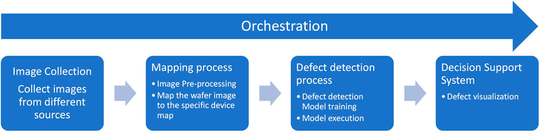
FIGURE 1. A generic approach for defect detection process.
The aforementioned approach is applied to two different types of wafer images, provided by the manufacturer’s vision inspection infrastructure: 1) low resolution wafer images and 2) high resolution images taken with a microscope. Although the proposed methodology is the same for both image types, different approaches are applied for the mapping and defect detection processes, driven by the different peculiarities of each step. A detailed analysis of these approaches is presented in the next sections.
Low resolution defect detection refers to an initial wafer inspection, using an image of the wafer revealing its grating. This was requested by the manufacturer from its suppliers as an initial screening stage, prior to executing the next steps. Note that the grating is embedded into the top cladding and is not visible at the end of the device fabrication. Thus, this image is the single source of information about the grating aspect. A typical example of such an image is shown in Figure 2-LEFT. Since the image is captured at an unspecified angle each time, the superposition with the wafer mapping is not apparent. The first step to this mapping is to account for the perspective of the image, as well as the lens distortion of the camera. This is performed using the Hugin open-source software (Conversion, 2022). The final image is shown in Figure 2-RIGHT, revealing a well-aligned wafer, ready for the next step of mapping the wafer map onto this image.
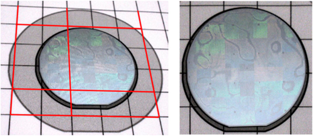
FIGURE 2. LEFT: Original wafer image. The red lines are drawn as guides for the perspective correction tool. RIGHT: Wafer image after the perspective and lens correction. The grating is visible as straight lines running vertically down the wafer.
Prior to performing the actual mapping process, a pre-processing stage is first applied. This consists of two steps; the first is the image “normalization” i.e., resizing of the grating image to a nominal size. This is done to reduce the computational load and memory requirements of the algorithm. The grating image is resized to match the nominal image dimensions of 2,667 × 2,739 pixels. Since we want to preserve the aspect ratio, only one dimension is scaled to exactly match the nominal one, leaving the other to follow accordingly.
The second step is the reconstruction of the wafer map and the creation of a raster image which matches the normalized grating image dimensions. The information of the wafer map contains the coordinates of the rectangular shapes of the devices. The rectangles are inserted into the raster image using image drawing primitives. The resulting image, an example of which can be seen in Figure 4-Left, is used in the registration tool, along with the normalized grating image. Following the registration, the transformation is altered in order to take into account the normalization step. The entire process is seen in Figure 3.
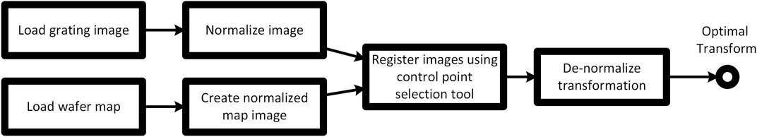
FIGURE 3. Overview of the mapping process for the grating image.
The mapping process, as is currently performed by the manufacturer, consists of manually overlaying the vector image of the map onto the grating image, using software such as Inkscape. This manual registration is facilitated by the alignment marks on the wafer. Even so, these marks are often obscure, coinciding with defected areas, and change in appearance, size and location in each wafer. Thus, automatic registration will be prone to detection failure, leading to erroneous results. This was also experimentally observed during the research and development process. The image processing algorithms and filters were not robust enough to ensure a high rate of success across different wafers, and were easily fooled by different illumination of the images, different colour hues, noise in the image, geometry of the marks etc. It was thus decided to follow a semi-autonomous registration process, where the user would be involved as little as possible, but importantly enough to accommodate the process.
The implemented process takes corresponding point pairs across two images, and computes the geometric transformation which, when applied to one image, is warped in such a way so as the selected points coincide (or their distance error is minimized, more accurately). This registration process is well known and supported off-the-self by various image processing libraries. We have deployed MATLAB’s dedicated tool, which allows one to inspect the two images of interest simultaneously, and select the point pairs. A screenshot of this control point selection tool is presented in Figure 4.
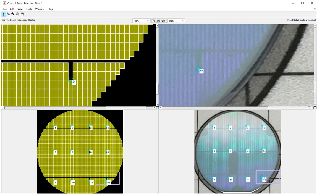
FIGURE 4. View of the Control Point Selection Tool. The raster image of the wafer map (left) and the grating image (right) for the wafer are clearly visible. The corresponding control pairs are marked with numbers 1 to 12.
Using this tool, a set of pairs is selected, which is then fed to an appropriate function that calculates a non-reflective similarity transformation between those points. This transformation assumes that the two images differ by a combination of translation, rotation, and scaling. The resulting transformation can then be used to map pixels from the grating image, to points in the wafer map, and thus identify devices which include defects.
The machine learning-based defect detection solution is focused on defect identification on the wafer parts and produces a new wafer image where the defective parts are highlighted. Specifically, this module includes the image collection with image pre-processing, the labelled data creation (annotation of images) via the COCO Annotator (Gygli and Ferrari, 2020) (Figures 5 – TOP ROW) and the deployment of deep learning algorithms for image defect segmentation (Tabernik et al., 2020). In the integrated defect detection pipeline, as soon as this module receives the perspectively corrected image, it inputs it to the trained segmentation model. This model has been developed with the aim to detect any possible defective spots and grating on the wafer image and produce a segmentation mask, with the different categories of classes represented with distinct colours. The final step in this process is to forward the result to the Decision Support System for inspection by the user. An example of this case can be seen in Figure 5 (BOTTOM ROW) where the marked image is presented.
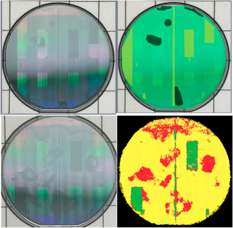
FIGURE 5. TOP ROW: Original wafer image (left) and annotated image (right). BOTTOM ROW: Original wafer image (left) and corresponding defect detection result (right).
After the reception of the processed wafer, the manufacturer’s staff checks the fabrication quality following a dedicated procedure, which includes the recording of high resolution images of the wafer surface. This is done using a Sensofar microscope with a 5x magnification objective. For imaging an entire 2-inch wafer, the Sensofar microscope records about 400 images that are then stitched together with a dedicated software. The resulting wafer scan image is then normalized (20,000 × 20,000 px, jpeg format with 0.75 quality factor) yielding a rasterized image with a typical size of about 100 MB. An example of such an image can be seen in Figure 6-Left, along with an image of a single device, (Figure 6-Right), which is taken after zooming into the initial wafer image. These images provide indeed a very detailed view of the wafer as well as each device and defects are clearly revealed. Interestingly, the image quality is high enough to localize each cell in the wafer and to see the ones impacted by a given defect. To be useful, this information must be registered and easily accessible, i.e. stored in a database, together with the other relevant laser properties. This task cannot be done manually since it is too time consuming and prone to registration errors. Thus, combining a machine learning-based defect detection algorithm with an automated device to defect mapping, greatly simplifies the process.
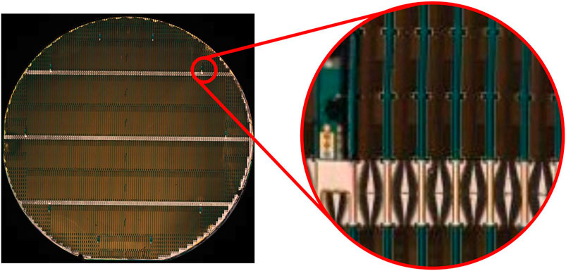
FIGURE 6. Surface scan of a wafer and blow-up of a region. The zoomed-in area is telling of the ultra-high resolution of the image.
In this task, we have to register the wafer map onto an ultra-high resolution surface scan of a wafer. The resulting images range from 10,000 × 10,000 pixel dimensions, to 20,000 × 20,000 and up. Loading these images into memory for processing, results in a significant allocation of blocks e.g. a 10,000 × 10,000 uncompressed image with a 32bit color depth pixel leads to about 381 Mb of memory while a 20,000 × 20,000 image requires 1.5 GB. These values are the bare minimum and in reality the requested memory is quite larger due to non-sequential allocation, memory segmentation, meta-data loaded for the image etc. From tests during the development stage, it was decided to resize the images to a “nominal” dimension which would not bottleneck the system.
Due to the high resolution of the wafer scan, it is possible to see each individual device on the image. The devices are delineated by the dark blueish bands that run vertically on the image, while their horizontal boundaries run through the crosses/junctions, as seen in Figure 7. The wafer map describes the boundaries of each device, given by the four corner points (red dots in Figures 7– left) in a counter-clockwise fashion. These dots/points are exactly located on the cross junctions (Figures 7– right). This dictates the strategy of registering the map to the image; detect the crosses in the image, extract the dots and map them to the unique points of the map. Essentially, this will create two sets of 2D point clouds for which we must find a geometric transformation that involves only translation, rotation, uniform scaling, or a combination of those, which creates an optimal “fit” between them, according to some measure i.e. bring them as “close” as possible. This is known as the Procrustes problem (Gower and Dijksterhuis, 2004) and in the planar case has 4 degrees of freedom (2 for translation, 1 for rotation and 1 for uniform scaling). Given the fact that each wafer can contain many hundreds of devices, leading to thousands of corner points, this will require searching a 4D space and many thousands of point pairs to elucidate an optimal fit. However, due to implicit assumptions in the entire imaging (and map creation) process, we can solve each sub-transform of the Procrustes map as a separate–and simpler-problem. For example, we know that the cross points should align vertically and thus fall on vertical straight lines. This can be checked in the surface scan image, and compensate for possible rotations.
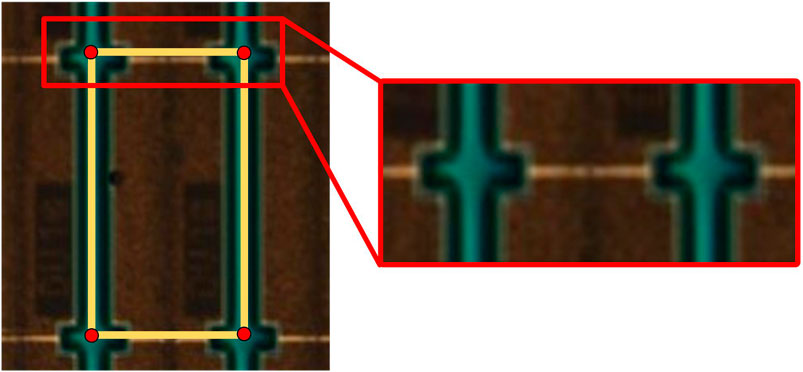
FIGURE 7. Depiction of a device, as seen on the surface scan image, and its abstraction as a rectangle in the map (yellow lines). Its edges are located at the crosses, seen on the right.
An overview of the various steps of the mapping process is seen in Figure 8. In the following, we will analyse each block separately, and see examples of the intermediate steps of the process, as well as final results using actual surface scans.
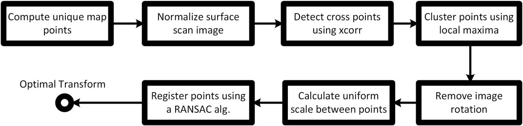
FIGURE 8. Overview of the mapping process for the surface scan image.
The initial steps consist of computing the unique points of the map that comprise the device rectangles, and the “normalization” i.e. resizing, of the surface scan image to a nominal size and some color processing. Specifically, let N be the set of nominal map points which must be registered on the image. If N contains |N| points, this number serves as a target value for the number of points that must be identified on the wafer image. The normalization step has a twofold purpose; first it reduces the computational load of the algorithms, making the mapping process tractable, and second, it is needed since the next steps are dependent on the image resolution and profile. Thus, image features which may vary greatly in size, will not be detected, leading to poor results. The following tasks refer to the actual detection of the cross points on the image. To accommodate this, a common technique in image processing has been used, namely the detection of a pre-set feature using cross-correlation. Cross-correlation is a measure of similarity of two signals as a function of the displacement of one relative to the other. This is also known as a sliding dot product or sliding inner-product. It is commonly used for searching a long signal for a shorter, known feature (Briechle and Hanebeck, 2001). In our application, the reference signal was a region-of-interest cut out from the wafer image, containing a cross junction (Figure 9-Top). Since we are interested in the morphology of the reference feature only, the color information is irrelevant. To this end, both the feature and the wafer scan images have been binarized i.e. converted into images containing only black and white pixels. Since binarization is applicable only to grayscale images, they have been converted to such by casting them to the HSV colorspace and keeping only the luminance plane (the V values). Examples of the binary image of the feature and the wafer scan, are given in Figure 9-Middle.
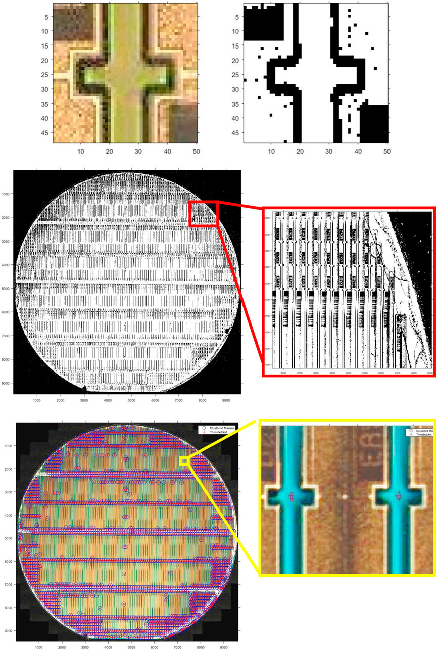
FIGURE 9. TOP: Reference feature used for detection (left). Its binary image is seen on the left. MIDDLE: Binary image of the test wafer and blow-up of a region showing individual devices. BOTTOM: Clustering of the test wafer and blow-up region depicting two clusters.
Following the binarization, the normalized cross correlation between the feature and the scan images is calculated. This produces a matrix r with values between 0 and 1, and the same dimensions as the scan image. Essentially for each pixel of the scan image, the corresponding element of r indicates the similarity of this pixel’s neighbourhood to the reference feature. A value of “1” means that the neighbourhood matches exactly the feature, while a value of “0” indicates complete dissimilarity. Apparently, we want to select only the pixels with a large enough value, by applying a threshold on r. However a large value might lead to only a small number of selected points, while a low value might result in many false positives. Furthermore, neighbouring pixels usually contain similar cross-correlation values since the values generally change smoothly.
To produce an “optimal” set of points, we resort to an iterative heuristic algorithm, which tries to find a suitable threshold for r, while at the same time clustering the resulting points. More thoroughly, the algorithm returns the local maxima of matrix r, each within a specified neighbourhood. It searches for such a threshold that when applied on r, the points above that threshold are clustered into neighbourhoods of a given radius, and the number of resulting points are at most within a specified tolerance of the number of nominal map points
In our tests, we have set a 5% tolerance for the number of clustering points and a 50 pixel radius for the clusters. If the algorithm doesn’t converge to the required number of clusters after 100 iterations, it terminates and outputs the current clusters. A clustering operation for the wafer is presented in Figure 9 - Bottom. The points resulting from the thresholding are seen as red crosses on the left image. The cluster maxima are depicted as blue circles. The clustering process is more obvious on the right image, where it can be seen that the thresholded points create close neighbourhoods (red crosses). The clustering then selects the point with the maximum cross-correlation value, among each neighbourhood (blue circles). The final output from the clustering process is a set of points M, which correspond to the device coordinates. The next steps of the mapping process are then to map this set M to the nominal map points N. Note that their number is not the same, thus there is no apparent one-to-one correspondence.
As stated earlier, detecting, and removing, a possible rotational component of the surface scan image, accounts for the 1 degree-of-freedom of the Procrustes transform, and significantly reduces the search space. Although the surface scans appear to be vertically aligned, at closer inspection, and after various trials, it was discovered that the images are actually rotated by an amount that varies from −1⁰ to 1⁰. Even though this might seem small, the image dimensions are quite big and thus a very long line rotated by a small angle, will present a large deflection at its edges. The detection of the image rotation is performed by applying the Hough transform on the data set M. The Hough transform (Cantoni and Mattia, 2013) is the de facto method for detecting lines in images and point clouds. After detecting the rotational component, the image is counter-rotated in order for the points to align finer, both vertically and horizontally.
Having the two data sets rotationally aligned, the next step is to compensate for their scale, i.e. find a multiplication factor such that when applied on one of the data sets, the two then differ only by a translation factor. Following the steps from the Procrustes analysis, we first remove the translational component from each set by subtracting their mean, i.e. geometric centroid, from each coordinate. Thus, if the set contains k points, {xi,yi}, i = 1...k, then its centroid is,
and the translated points are,
This centres the two data sets on (0,0), and by applying a uniform scale, their centre remains invariant. To find the scaling factor, we resort to the intraset distances. The idea is that since the two data sets differ by a scaling factor, the relative distances between their points, per set, should follow a similar distribution among sets. Given that the points lie on a regular grid, the mode i.e. most frequent value of these distributions should correspond to the same physical distance. Thus, let
be the intraset distance distributions for each set. Then, the scaling factor for each set is,
By dividing each point with the respective scaling factor, the sets are normalized such as the most frequent distance between their points is “1”. The new normalized sets are denoted as
To compensate for the translation component of the two normalized data sets, we run a Random Sample Consensus (RANSAC) algorithm (Derpanis, 2010). RANSAC is an iterative method to estimate parameters of a mathematical model from a set of observed data that contains outliers, when outliers are to be accorded no influence on the values of the estimates. It is a non-deterministic algorithm in the sense that it produces a reasonable result only with a certain probability, with this probability increasing as more iterations are allowed. A basic assumption is that the data consists of “inliers”, i.e., data whose distribution can be explained by some set of model parameters, though may be subject to noise, and “outliers” which are data that do not fit the model. The outliers can come, for example, from extreme values of the noise or from erroneous measurements or incorrect hypotheses about the interpretation of data. RANSAC also assumes that, given a (usually small) set of inliers, there exists a procedure which can estimate the parameters of a model that optimally explains or fits this data.
Applied to our specific problem, let
and we apply this translation on
The total cost for the particular
By iterating over all pairs in S, we get the optimal pair which minimizes the cost C. This implementation of the RANSAC algorithm is called “Maximum Likelihood Estimation Sample Consensus” MLESAC (Torr and Zisserman, 2000) and provides more robust performance and better results than the standard format.
Selecting the number of random pairs which comprise S, is crucial for finding a good fit. Apparently, the maximum number of pairs is
By applying this bounding condition on all pairs, we get the subset of valid pairs
If
To register the two sets, this translation is applied to each point
For each point in
The final registration map is conceived by combining the rotation, scale and translation components, calculated in the previous sections. The registration for the test wafer is presented in Figure 10.
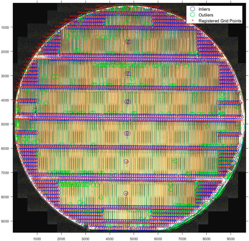
FIGURE 10. Final registration for the test wafer.
Following the mapping process, the defect detection algorithm is then applied on the corrected image. Defect detection is performed using image processing primitives such as template matching, thresholding, morphological operations, and edge detection. The methodological goal is to assess the quality of the waveguide of the optoelectronic wafer devices in terms of detecting potential discontinuities. The steps taken in this module are summarised as follows.
Stage 1: the image is received and goes under two pre-processing stages by correcting its rotation and performing median filtering for better highlight of the region of interest.
Stage 2: Template matching is performed by comparing a template that represents a non-defected waveguide with the inspected waveguide, as a first check.
Stage 3: Thresholding and morphological operations are applied to the binarized image, which is then smoothen as a preparation step for the edge detection part.
Stage 4: Edge detection is performed to count the number of edges on the waveguide as a second check.
Template matching is considered one of the pattern recognition techniques (Ebayyeh and Mousavi, 2020). In automatic optical inspection applications, the template matching algorithm starts by first identifying a reference template which usually represents the normal non-defected case (also known as golden template) which can be used for comparison. The chosen template is then compared to the inspected samples using different types of correlation functions. In our case, a template of non-defected waveguide was selected as shown in Figure 11-Top. This template is compared to other inspected samples of QCL devices using Pearson correlation coefficients (PCC) (Zhong et al., 2015) given by the equation,
where
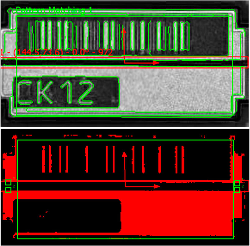
FIGURE 11. (TOP) Template matching process. The golden template is the black waveguide, seen inside the red rectangle in the middle of the optoelectrical device (BOTTOM): Binarized image for edge detection.
At the next stage, thresholding and morphological operations on the image generate a binarized image which allows the analysis of the waveguide’s edges. Edge detection is used to find boundaries and sharp edges, and can be performed by locating the discontinuities in pixel intensities using specific filters and operators (Ebayyeh and Mousavi, 2020). Here, we have employed the Canny filter in order to distinguish the edges of the waveguide. Depending on the number of edges found, the waveguide can either pass or fail this stage. Figure 11–Bottom illustrates the result of binarizing the image, applying morphological operations and finding the edges.
A logical conjunction operation was used for the result of the template matching and edge detection as a rule-based decision to specify whether the device is defected or not. If the waveguide has passed both checks successfully, the device is labelled as “Pass”. Otherwise, if one or both checks was not successful, the device is labelled as “Fail”.
Architecturally, the solution consists of sub-services developed by individual technology providers and communication via a common bus, implemented through a Higher Level Communication Middleware (HLCM). The backbone of the integrated solution is the HLCM which follows a standard micro-service architecture and acts as an orchestrator of the whole integrated system. Figure 12 shows the abstract flow of information from end to end, as well as the internal structure of the HLCM so that the overall data path can be understood. This information flow is applied in both wafer image types (low resolution and high resolution images). Distribution of data is accomplished by publishing and subscribing to topics of an MQTT broker. A description of this data for every step is given below.
• The process starts with the publication of images by the manufacturer through the MQTT broker of the HLCM on a predefined topic.
• The data through the Data Source Plugin, which is attached to the Data Provider micro-service, are aggregated and relayed to the service which is responsible for the mapping of the wafer devices process. Two different mapping processes are implemented; one for each wafer image type according to the proposed methodology. The mapping processes subscribe to a specific topic of the HLCM, fetch the uploaded images and the device wafer topology, process it and publish the generated transformation matrix to a specified topic.
• Through the Transformer micro-service, the data are delivered to the service that is responsible for the detection of the defected devices on the wafer. Similar to the previous step, two different defect detection processes are implemented; one for each wafer image type (image based defect detection for high resolution images and machine learning based detection for low resolution images). The detection processes subscribe to a specific topic of the HLCM and fetch the image, enhanced with the transformation matrix. After processing they generate the defect map of the wafer.
• The outputs of both analyses are transferred through the HLCM to the Decision Support System, which combines the various inputs and provides a user-friendly interface to the manufacturer engineers for identifying the problematic devices.
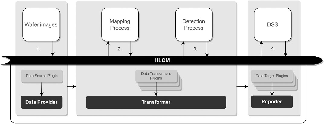
FIGURE 12. Overview of the solution pipeline.
The next sections describe the various components used in this implementation.
HLCM has the responsibility of acquiring data and distributing it. HLCM follows a standard micro-services architecture, where all the functionality is implemented in distinct micro-services and the communication between the services is done through a central bridge (MQTT Broker). For each microservice, one or more plug-ins have been implemented for the individual processes that take place. The micro-services that have been implemented are the following:
• Data Provider: Data Provider is a tool responsible for periodically fetching data from a specific data source to the Event Bus (by publishing on a specific topic).
• Transformer: This module is responsible for transforming incoming data. These data can be transformed if it is required from the use case, and formatted to fit the expected JSON format. Then, they are transferred to the relevant data targets by using the Message Bus.
• Reporter: Reporter is a micro-service that produces reports which include results. Incoming results arrive from different micro-services and the Reporter is responsible for collecting the results and delivering them to the internal or external destinations.
Finally, the HLCM provides a user-friendly interface to allow for task management and monitoring.
The two mapping processes have been interfaced with the appropriate servers to fetch and output the mapping information produced via their respective algorithms. These algorithms have been made to communicate with the HLCM via the MQTT protocol, in order to exchange their messages. Finally, to facilitate integration, the user experience has been augmented to enable a more streamlined operation. Thus, the algorithmic implementations of the mappings have been integrated with appropriate Graphical User Interfaces which manage the process of communication with the rest of the components, as well as the internal algorithmic modules of the mapping processes. The two programs have been packed for easy redistribution and installation on user computers, as separate stand-alone executables. Both algorithms have been “wrapped” with a similar program which handles input/output operations, error handling, logging and internal I/O with the mapping process. Defect detection component.
Regarding the integration of the segmentation model to the ecosystem of iQonic, a microservice architecture has been designed and implemented by leveraging containerization technologies such as Docker which allows each service to be independent and self-sufficient (Jaramillo, Nguyen and Smart, 2016). Specifically, a consumer service has been developed which subscribes to the respective topic on the HLCM that waits for data streams. The expected message contains the perspective corrected image of the grating, encoded and included in a JSON document. This image is extracted and pre-processed (resize, noise reduction, RGB-grayscale transformation) in order to be sent for inference. To deploy the model in production a base image has been developed that simulates the ML environment, wraps the model and exposes a trigger function that accepts the pre-processed image while providing as output (inference) the segmentation mask that highlights the defects on the received grading. Finally, this output is encoded and wrapped in a document (JSON) alongside with some relevant metadata and distributed back to the relevant services such as DSS through HLCM.
As mentioned in earlier, an image based approach has been chosen for detecting defects in high resolution images. This is implemented as a LabView application. Figure 13 depicts the front panel display of LabView. Through the UI, a user can select a specific image of a device contained inside the wafer. The application processes the device image and labels it as either “Pass”, if no failure is detected, or “Fail” if defects are detected.
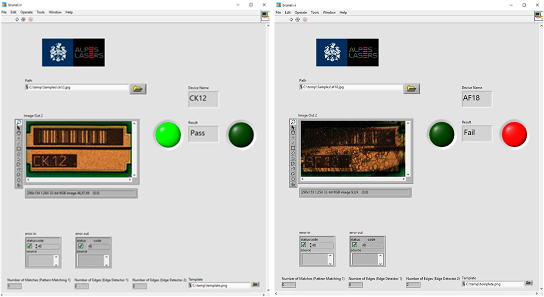
FIGURE 13. GUI that displays the device name along with device result (pass and fail cases).
In order to integrate the defect detection application with the entire iQonic system and automate the detection process, a process execution engine (PEX) has been developed which can crop the high resolution wafer scan image into several smaller ones that depict the individual devices inside the wafer. For each device image it executes the application, acting as a wrapper, providing labelling. The PEX follows the same micro-service architecture as HLCM, and adopts enterprise application messaging patterns. The main functionality of the PEX, is to create and manipulate data flows between a data provider and a data consumer, applying a transformer to the streamed messages.
The last step of the pipeline is the combination of the outputs from mapping and defect detection processes for both wafer images, into a user-friendly web interface, which manufacturer engineers use to identify the good, or faulty, parts of the wafer and the respective devices. As it is presented in the previous sections, mapping and defect detection processes run independently, processing the images provided by the manufacturer. The results are aggregated, transferred through the HLCM and persisted at the DSS, which provides a user interface, where results can be filtered by wafer and/or device id and visualised in an interactive interface based on the wafer device map.
Figure 14, presents the implemented DSS user interface, where a grid with the mapped devices is presented on top of the marked image, providing the filtering functionality to detect the problematic devices. An interactive view of the fusion of the wafer image and the machine learning detection results is presented to the end-users via the DSS. The view is created by encoding the detection results as an RGB image, centering an SVG graphical representation of the wafer’s device map using the transformation matrix and subsequently is placed on a UI area, which is interactive through the use of Javascript and HTML. The inverse transformation matrix is used to map the separate devices to regions in the machine learning detection result and to estimate the degree of defects for each device obtained by filtering in the mapped pixel region for the encoded pixels indicating a defect. The defect indicative and no defect indicative ratios of the pixels that belong to each device are used to categorize the device as defected. In addition, a filter for categorizing the affected devices is given to the end user by selecting a threshold of the destruction rate of each device that is acceptable to the user. Alternatively, users can rank all the devices by the number of defected pixels within the mapped image region. Finally, following the defect status assignment, the DSS visualizes and reports the results to the final user and/or disseminates them to other connected services.
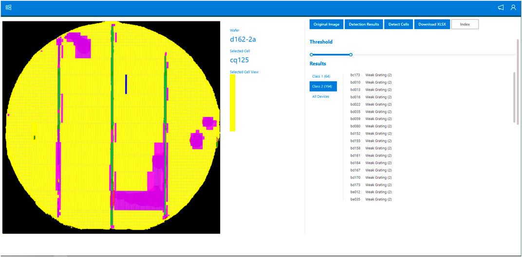
FIGURE 14. Decision Support System UI web interface.
The second process of the manufacturer use case and scenario for faulty device identification produced on a microscope, are actually the wafer scan images in Quantum Cascade Laser fabrication used for the analysis. The wafer should be segmented to show the device in each segment where three types of classes are being investigated after this step, i.e., normal, dirt and defect. The normal class represents devices that do not have any defect type and are considered eligible for further manufacturing process. The dirt class represents the devices that contain dirt in a form of large black spots. Such devices can be investigated thoroughly on each case basis. Hence, it can be either accepted or rejected depending on the severity of dirt. Finally, the defect class, this class represents the devices with defects and can be identified by the discontinuity of the laser path. In this process, the same device mapping technique as it is already presented in the previous process is used while the defect identification process is applied. As such, the final data analysis of the defect prediction and classification results of the wafer segments, i.e., normal, dirt and defected wafer segments are sent to DSS through the HLCM.
As it is expected, defects are detrimental to the performance of the quantum cascade lasers. However, depending upon their nature and severity, different properties of the lasers can be impacted. In this section, we discuss preliminary results regarding the impact of the developed tools upon the production of such optical devices. This evaluation is performed by comparing the predictions of the presented algorithms with real physical data recorded during the production of quantum cascade lasers by the manufacturer. This is a blind experiment, since the lasers have been tested without prior knowledge about the algorithm classification results, meaning that lasers with different classification status are included in this study.
The irst use case is focused on the analysis of defects occurring during the grating fabrication. The purpose of the grating is to force a monomode emission and, for this reason, it is meaningful to compare the monomode range (derived from the optical tests performed by the manufacturer) and the degree of defect associated with the device by the analysis algorithm. This comparison was done for hundreds of lasers from several wafers, showing a good correlation between the reduction of the monomode range and an increase of the grating defect rate. For some wafers, it was found that the devices with the highest defect rate are not able to produce a monomode emission, meaning that the grating does not provide the expected feedback for the mandatory laser mode selection. Globally, the monomode range for devices with no grating defect is three times larger than for devices tagged with a defect rate of 100%, as shown in Figure 15, LEFT panel. In other words, a healthy device covers a much larger frequency range and has a higher probability to meet the requirements for a specific application, as targeting a specific molecular vibration band for example. From a production point of view, mounting and testing only devices with healthy grating only will drastically reduce the work required to obtain a laser with a monomode emission at a specific emission frequency and the total laser production cost.
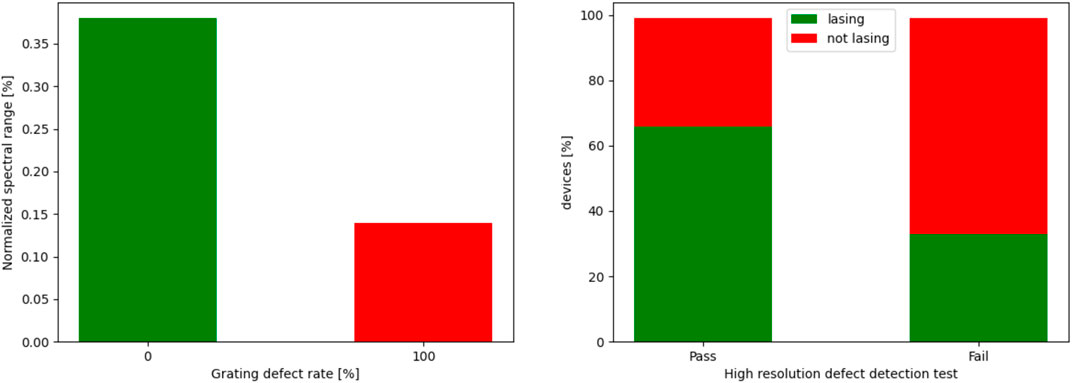
FIGURE 15. Comparison between the algorithm predictions and measurements performed on real devices. LEFT: Averaged normalized spectral range for devices identified with 0 and 100% grating defect rate, respectively, for the test wafer. RIGHT: Percentage of lasing devices tagged “Pass” and “Fail” by the high resolution image algorithm for the test wafer.
The second use case concerns the analysis of high-quality images of the devices’ surfaces recorded with Sensofar microscope. In this case, the impact on the device operation can be even more dramatic than in the use case discussed previously. Indeed, the aim here is to automatically detect discontinuities along the laser ridge, which can clearly prevent the corresponding device from lasing. About 50 lasers from the test wafer have been mounted, including cells tagged as “Pass” and “Fail” and the optical response of the lasers characterized following the standard manufacturer’s production procedure. These lasers have been classified in two categories: “valid” for the devices able to lase in the continuous regime, and “invalid” for the devices not able to lase in the continuous regime. The two classification sets have been compared, showing that two thirds of the lasers have been successfully classified by the decision algorithm (Pass/valid and Fail/invalid). That means that a laser from the “Pass” category has a probability to be valid, two times higher than that of a laser from the “Fail” category, as shown in Figure 15, RIGHT panel. Note that the invalidity of a laser can clearly be caused by a defect not visible on the recorded images, for example due to a defect in the cladding.
All-in-all, combining the two defect detection schemes discussed herein, a laser classified in the “Pass” category with a 0% defect rate for its grating, has a probability six times higher to lase at a specific frequency than a laser classified in the “Fail” category, with a 100% defect rate regarding its grating evaluated score. On the basis of this information, it is then possible to define cleaving and mounting strategies to target the most promising chips, in order to reduce the production costs.
This research describes an industry 4.0 concept approach for wafer-level defect detection on optoelectronic devices and presents an innovative integrated solution. Current market trends were considered in the design and implementation of the current work in order to create an innovative end-to-end solution for the optoelectrical sector. The system comprises a monitoring tool for the life cycle of optoelectronic devices, as well as image processing and deep learning algorithms. Defect identification has been automated utilizing two image-based defect detection pipelines that use low-resolution grating pictures and high-resolution surface scan images, respectively. The communication middleware orchestrates the image processing, transporting the information through the different processing phases all the way to the DSS. All acquired data is labelled with additional defect type classification, resulting in device maintenance advice for the optoelectronic engineer. End users evaluated this authentic laser manufacturing sector use case as well as the solution implementation. The initial results appear to fulfil end-user expectations while showing positive outcomes as the analysis showed that combining the two defect detection systems presented, a laser classed as “Pass” with a zero percent defect rate for its grating has a six-fold higher likelihood of lasing at a certain frequency than a laser categorized as “Fail” with a 100 percent defect rate for its grating evaluation score. This is considered by the end user to be already a huge benefit of the iQonic zero-defect-manufacturing approach applied to its QCL manufacturing, as fail-classified components will not enter a long and high value adding manufacturing sequence, and thus not compromising yield.
Furthermore, sub-sequent cleaving and mounting techniques may be developed to target the most promising chips and lower manufacturing costs. The iQonic system will be fine-tuned in the near future, as it is recognized that the entire system potential may match the end-user’s goals and motivations for enhanced dependability, availability, performance, quality, and cost savings. As a result, continuous improvements to the collaborative system are anticipated in the near future.
The datasets presented in this article are not readily available because they contain confidential industrial data. Requests to access the datasets should be directed to bWlsZW5rb3ZpY0BhYmUuZ3I=.
GM, GK, JM contributed to the preparation and submission of the manuscript. GM, GK contributed to the mapping process, SF, GF, AC contributed to the machine learning based defect detection, AA, AMo contributed to the image-based defect detection, KA, JM, ZC contributed to the DSS and HLCM development, EB contributed to the ZDM aspects of the paper, JB, SB, OL, AMü evaluated the solutions.
This project has received funding from the European Union’s Horizon 2020—the Framework Programme for Research and Innovation (2014–2020) under grant agreement No 820677—Innovative strategies, sensing and process Chains for increased Quality, re-configurability, and recyclability of Manufacturing Optolectronics (iQonic).
Authors GM and GK are employed by SENSAP Swiss AG. Authors SF, GF, and AC, are employed by CORE Innovation. Authors KA, JM, and ZC are employed by ATLANTIS Engineering S.A. Authors JB, SB, OL, and AMü are employed by Alpes Lasers SA.
The remaining authors declare that the research was conducted in the absence of any commercial or financial relationships that could be construed as a potential conflict of interest.
All claims expressed in this article are solely those of the authors and do not necessarily represent those of their affiliated organizations, or those of the publisher, the editors and the reviewers. Any product that may be evaluated in this article, or claim that may be made by its manufacturer, is not guaranteed or endorsed by the publisher.
Abramov, P. I., Kuznetsov, E. V., Skvortsov, L. A., and Skvortsova, M. I. (2019). Quantum-cascade lasers in medicine and biology (review). J. Appl. Spectrosc. 86, 1–26. doi:10.1007/s10812-019-00775-8
Anantathanasarn, S., Srisaard, T., Wattanarat, J., and Budsayaplakorn, N. (2019). “AI in laser diode module manufacturing,” in 2019 IEEE international conference on consumer electronics-asia (ICCE-Asia) (Bangkok, Thailand: IEEE), 168–169.
Bismuto, A., Blaser, S., Terazzi, R., Gresch, T., and Muller, A. (2015). High performance, low dissipation quantum cascade lasers across the mid-IR range. Opt. Express 23, 5477. doi:10.1364/oe.23.005477
Briechle, K., and Hanebeck, U. D. (2001). “Template matching using fast normalized cross correlation,” in Optical pattern recognition XII vol-4387 (München, Germany: International Society for Optics and Photonics), 95–102. doi:10.1117/12.421129
Cantoni, V., and Mattia, E. (2013). “Hough transform,” in Encyclopedia of systems biology. Editors W. Dubitzky, O. Wolkenhauer, K. H. Cho, and H. Yokota (New York, NY: Springer). doi:10.1007/978-1-4419-9863-7_1310
Chang, M., Chen, B., Gabayno, J., and Chen, M. (2016). Development of an optical inspection platform for surface defect detection in touch panel glass. Int. J. Optomechatronics 10 (2), 63–72. doi:10.1080/15599612.2016.1166304
Conversion, G. (2022). “Hugin,” in SourceForge (Slashdot Media). [online]. Available at: https://sourceforge.net/projects/hugin/(Accessed May 11, 2022).
Ebayyeh, A., and Mousavi, A. (2020). A review and analysis of automatic optical inspection and quality monitoring methods in electronics industry. IEEE Access 8, 183192–183271. doi:10.1109/access.2020.3029127
Ferretti, S., Caputo, D., Penza, M., and D'Addona, D. M. (2013). Monitoring systems for zero defect manufacturing. Procedia CIRP 12, 258–263. doi:10.1016/j.procir.2013.09.045
Gower, J., and Dijksterhuis, G. (2004). Procrustes problems. United Kingdom: Oxford University Press. Retrieved from: https://oxford.universitypressscholarship.com/view/10.1093/acprof:oso/9780198510581.001.0001/acprof-9780198510581 (Accessed May 16, 2022).
Gygli, M., and Ferrari, V. (2020). Efficient object annotation via speaking and pointing. Int. J. Comput. Vis. 128 (5), 1061–1075. doi:10.1007/s11263-019-01255-4
Harrer, A., Szedlak, R., Schwarz, B., Moser, H., Zederbauer, T., MacFarland, D., et al. (2016). Mid-infrared surface transmitting and detecting quantum cascade device for gas-sensing. Sci. Rep. 6, 21795. doi:10.1038/srep21795
iQonic-H2020 (2022). Iqonic H2020. [online]. Available at: https://www.iqonic-h2020.eu/(Accessed May 13, 2022).
Isensse, K., Kröger-Lui, N., and Pertrich, W. (2018). Biomedical applications of mid-infrared quantum cascade lasers – A review. Analyst 143, 5888–5911. doi:10.1039/c8an01306c
Jaramillo, D., Nguyen, D. V., and Smart, R. (2016). “Leveraging microservices architecture by using Docker technology,” in SoutheastCon 2016 (Norfolk, VA, USA: IEEE), 1–5.
Mourtzis, D., Angelopoulos, J., and Panopoulos, N. (2021). Equipment design optimization based on digital twin under the framework of zero-defect manufacturing. Procedia Comput. Sci. 180, 525–533. doi:10.1016/j.procs.2021.01.271
Mourtzis, D., Angelopoulos, J., and Panopoulos, N. (2022). Operator 5.0: A survey on enabling technologies and a framework for digital manufacturing based on extended reality. J. Mach. Eng. 22, 43–69. doi:10.36897/jme/147160
Mourtzis, D., and Doukas, M. (2014). Design and planning of manufacturing networks for mass customisation and personalisation: Challenges and outlook. Procedia Cirp 19, 1–13. doi:10.1016/j.procir.2014.05.004
Psarommatis, F., May, G., Dreyfus, P. A., and Kiritsis, D. (2020). Zero defect manufacturing: State-of-the-art review, shortcomings and future directions in research. Int. J. Prod. Res. 58 (1), 1–17. doi:10.1080/00207543.2019.1605228
Psarommatis, F., Sousa, J., Pedro Mendonça, J., and Kiritsis, D. (2022). Zero-defect manufacturing the approach for higher manufacturing sustainability in the era of industry 4.0: A position paper. Int. J. Prod. Res. 60 (1), 73–91. doi:10.1080/00207543.2021.1987551
Schlosser, T., Beuth, F., Friedrich, M., and Kowerko, D. (2019). “A novel visual fault detection and classification system for semiconductor manufacturing using stacked hybrid convolutional neural networks,” in 2019 24th IEEE international conference on emerging technologies and factory automation (ETFA) (Zaragoza, Spain: IEEE), 1511–1514. doi:10.1109/ETFA.2019.8869311
Tabernik, D., Šela, S., Skvarč, J., and Skočaj, D. (2020). Segmentation-based deep-learning approach for surface-defect detection. J. Intell. Manuf. 31 (3), 759–776. doi:10.1007/s10845-019-01476-x
Torr, P. H., and Zisserman, A. (2000). Mlesac: A new robust estimator with application to estimating image geometry. Comput. Vis. image Underst. 78 (1), 138–156. doi:10.1006/cviu.1999.0832
Keywords: industry 4.0, zero defect manufacturing, decision support system, wafer device, optoelectronics, machine learning, computer vision
Citation: Moustris GP, Kouzas G, Fourakis S, Fiotakis G, Chondronasios A, Abu Ebayyeh AARM, Mousavi A, Apostolou K, Milenkovic J, Chatzichristodoulou Z, Beckert E, Butet J, Blaser S, Landry O and Müller A (2022) Defect detection on optoelectronical devices to assist decision making: A real industry 4.0 case study. Front. Manuf. Technol. 2:946452. doi: 10.3389/fmtec.2022.946452
Received: 17 May 2022; Accepted: 04 July 2022;
Published: 22 August 2022.
Edited by:
Foivos Psarommatis, University of Oslo, NorwayReviewed by:
Nikos Panopoulos, University of Patras, GreeceCopyright © 2022 Moustris, Kouzas, Fourakis, Fiotakis, Chondronasios, Abu Ebayyeh, Mousavi, Apostolou, Milenkovic, Chatzichristodoulou, Beckert, Butet, Blaser, Landry and Müller. This is an open-access article distributed under the terms of the Creative Commons Attribution License (CC BY). The use, distribution or reproduction in other forums is permitted, provided the original author(s) and the copyright owner(s) are credited and that the original publication in this journal is cited, in accordance with accepted academic practice. No use, distribution or reproduction is permitted which does not comply with these terms.
*Correspondence: Jovana Milenkovic, bWlsZW5rb3ZpY0BhYmUuZ3I=
Disclaimer: All claims expressed in this article are solely those of the authors and do not necessarily represent those of their affiliated organizations, or those of the publisher, the editors and the reviewers. Any product that may be evaluated in this article or claim that may be made by its manufacturer is not guaranteed or endorsed by the publisher.
Research integrity at Frontiers
Learn more about the work of our research integrity team to safeguard the quality of each article we publish.