 Qian Heng1
 Yi Ding
94% of researchers rate our articles as excellent or good
Learn more about the work of our research integrity team to safeguard the quality of each article we publish.
Find out more
ORIGINAL RESEARCH article
Front. Energy Res., 02 April 2025
Sec. Smart Grids
Volume 13 - 2025 | https://doi.org/10.3389/fenrg.2025.1580823
This article is part of the Research TopicAdvancements in Power System Condition Monitoring, Fault Diagnosis and Environmental CompatibilityView all 16 articles
The power module package insulation is prone to partial discharge (PD) under fast square pulses, which is one of the main reasons for power module packaging failure. However, there are few studies on PD under square electrothermal coupling stress. One of the important reasons is that the electromagnetic interference and displacement current generated by the rising and falling edges of the square pulse seriously interfere with the detection of PD. To address this problem, this paper proposes a multi-spectral optical detection method with high sensitivity and strong anti-interference. Based on the multi-spectral synchronous detection platform, the high-temperature PD characteristics of power module package insulation under square pulses are studied. The results show that the partial discharge inception voltage (PDIV) decreases with increasing temperature, and the intensity of the PD multi-spectral signal increases with increasing temperature. In addition, the statistical analysis of the maximum optical signal intensity, cumulative optical signal intensity, number of PDs, and phase of PD under square pulse shows that with the increase of temperature, the maximum optical signal intensity and cumulative optical signal intensity of PD increase, and PD events mostly occur on both sides of the square pulse. Among them, the optical signal in the near-ultraviolet band is dominant, and the near-infrared signal has an obvious increase trend. These findings are of great significance for the reliability detection of power module package insulation.
Power devices are the core of power conversion and circuit control in electronic devices. The new generation of power electronic devices based on wide bandgap semiconductors (such as SiC and GaN) have higher breakdown voltage, faster switching speed, and lower switching loss (Hou et al., 2020), and are gradually being widely used in smart grids, electric vehicles, and new energy generation. However, with the long-term use of devices and the continuous increase in operating voltage and current, the reliability of power module packaging insulation is easily reduced. Partial discharge (PD) occurring in packaging materials (such as silicone elastomers) can cause material aging and even breakdown (You et al., 2021) and is one of the main causes of package insulation failure.
In most cases, the package insulation of the power module is under a unipolar high-frequency high-voltage square pulse (hereinafter referred to as a square pulse). Reference (Fabian, et al., 2005) pointed out that possible voids and local protrusions in the interface between ceramic and metal layers on DBC substrates can lead to local electric field enhancement, which is prone to partial discharge and electric trees. References (Mancinelli, et al., 2016) studied the effects of frequency and waveform on PDIV in silicone gels under sine and square wave voltages and found that the electrical branches grow faster in silicone gels under square wave voltages, but the square wave interference is more severe than the sinusoidal interference. When detecting PD under a square pulse, the displacement current and spatial electromagnetic interference (EMI) generated by the power module switch are the main interference sources. Conventional PD detection methods based on electrical pulses, electromagnetic waves, etc., may be strongly interfered with and cannot sensitively identify discharge signals (Zhang et al., 2020). Our previous research explored EMI suppression and PD extraction methods based on down-mixing technology, but the high cost of the device is not easy to use in practical engineering applications. References (Auge et al., 2013) Under AC sinusoidal and bipolar square wave high voltages, the partial discharge differences of ceramic substrates in power modules were investigated by the optical detection method, and it was found that the optical detection method can sensitively identify the discharge signal and has good anti-interference performance. Silicon photomultiplier arrays with high sensitivity, strong anti-interference, and small size show great application potential in this regard (Ren et al., 2020). Studies have shown that PD light radiation is accompanied by complex processes such as field emission, ionization, adhesion, and re-combination in the development of discharge. The light intensity at a specific wavelength is determined by the light radiation path and defect structure. The wavelength of corona discharge light is < 400 nm, mainly ultraviolet light; the wavelength of spark discharge light is between 400 and 700 nm, mainly visible light. The materials used for the insulation of power module packaging are mainly ceramics and potting compounds, which are different from gas insulation. Currently, there is very little research in this area. In addition, as high-voltage power modules are miniaturized, the electrical and thermal coupling stresses borne by package insulation are increasing (Ding et al., 2023). Studies have shown that the internal operating temperature of SiC-based power modules can reach above 200°C (Siow et al., 2015). Therefore, it is necessary to study the radiation spectrum characteristics of high-temperature PD of power module package insulation under square pulses.
In summary, this paper designs a multi-spectral optical sensing device for PD, which is capable of extracting the optical spectral information of PD signals across different wavelength bands. In addition, compared with the previously proposed down-mixing method, the designed multi-spectral sensing device is proven to be able to sensitively detect PD signals. In the experiment, multi-spectral signals of PD in the packaging insulation under unipolar square pulse voltage at different temperatures were recorded. This work can provide a reference for the reliability of power module packaging insulation.
The photons radiated from PD in packaging insulation cover a broad range of wavelengths from ultraviolet to infrared. Multi-spectral detection devices can be used to analyze the distribution of PD signals across different wavelength bands. This requires the sensor to simultaneously have high sensitivity, anti-interference capability, and the ability to measure PD light signals across different spectral wavelength ranges (Ren et al., 2016). Therefore, this built PD detection device is based on a silicon photomultiplier array (SiPM) with single-photon detection capability, using four bandpass filter groups and a 4 × 4 SiPM array distributed on the surface to form a 4-channel multi-spectral sensor. Each channel is an independent unit, with real-time synchronous output and no inter-reference. SiPM adopts a dense array form, integrating avalanche photodiodes to form a photoelectric sensor capable of detecting weak light signals. Compared with PMT, SiPM can achieve a signal gain of the order of 106 at a bias voltage of 30 V. It has the advantages of small size, fast response speed, and strong anti-interference capability, and can effectively detect photons in the wavelength range of 200∼900 nm. After the reverse bias voltage is applied, SiPM will be in a state of waiting for excitation and work in the “Geiger” mode (Ren et al., 2018). In this mode, once a photon contacts the SiPM surface, the photon will trigger a rapid collision of carriers, resulting in a self-sustaining charge avalanche, which in turn generates a light signal pulse. The circuit and physical diagram of the multispectral detection device are shown in Figure 1. The multispectral sensor, power supply unit, signal conditioning unit, etc., are integrated inside the metal shielding shell. Considering that the emission spectrum of partial discharge is mainly in the ultraviolet, visible, and infrared bands, the bands of the bandpass filters used are 250∼400 nm (B1), 400∼500 nm (B2), 500∼700 nm (B3), and 700∼800 nm (B4). The photo-detection efficiency (PDE) and the transmittance of the filter are shown in Figure 2, where PDE characterizes the average probability that a photon entering the array can trigger photoelectric conversion.
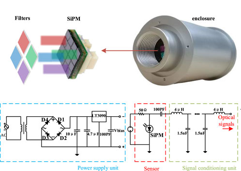
Figure 1. Physical diagram and circuit structure of multispectral optical detection device.
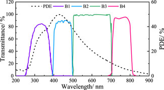
Figure 2. Filter transmittance and photodetection efficiency of the sensor.
Since the PDE of SiPM and the transmittance of the filter vary with wavelength, the signal directly output by the multi-spectral PD detection system cannot reflect their true value or proportional relationship. To solve this problem, a xenon lamp light source with a continuous spectrum in the 200∼2200 nm band is used to calibrate the PD signal of different bands output by the PD multi-spectral detection system. Considering the environmental factors of the test, the calibration experimental platform based on the xenon lamp is the same as the PD experimental platform (described below). At the same time, to accurately estimate the variation of different spectral components during the PD process, this paper has normalized and calibrated the signals of each band with the B3 band as a reference. The calibration steps are as follows: Place the xenon lamp at the same position as the test specimen in the cavity, illuminate the input end of the mul-ti-spectral detection system, measure the output photocurrent magnitude of each band, and then determine the correction coefficient of each band by comparing the measured value with the known xenon lamp spectrum, as shown in Equation 1.
Where

Table 1. Correction factors for different bands.
At the moment of rising edge and falling edge of high dV/dt squared pulse, the rapid change of electric field will produce electromagnetic interference. The spectrum of interference caused by square pulse is mainly distributed below 3 GHz, which will cause interference to electrical detection methods such as pulse current method, and ultra-high frequency (UHF) method. According to IEC 61934 standard, the overlapping spectrum between interference and PD signal can be eliminated by increasing the detection frequency and using high-pass filter. However, the increase of detection frequency leads to higher requirements for signal sampling and processing speed. To properly solve this problem, a down-mixing partial discharge detection method is proposed. First, the UHF signal is filtered through a high-pass filter to remove noise interference, then mixed with a fixed-frequency local oscillator signal, and finally passed through a low-pass filter to obtain the difference frequency signal. While retaining the basic characteristics of the original signal, the signal frequency band is reduced to the low-frequency region, which facilitates signal acquisition and improves the signal-to-noise ratio. Our research team has previously detailed the circuit principles and device parameters in their work (Wang et al., 2021) and has demonstrated that the PD detection system combining high-pass filters and down-mixing technology is effective in suppressing square pulse interference and detecting PDs.Figure 3 shows the circuit diagram and physical diagram of the down-mixing PD detection device, as well as the linear relationship between the down-mixing signal amplitude and the apparent discharge. Figure 3 shows the circuit diagram, physical diagram, and calibration result of the down-mixing PD detection device.
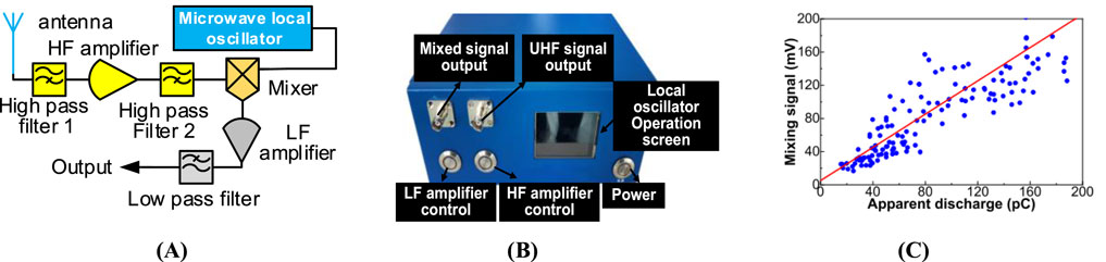
Figure 3. Down-mixing PD detection system. (A) Circuit diagram; (B) Physical picture; (C) Calibration result.
The PD test specimen used in the experiment is consistent with the typical power module packaging structure, as shown in Figure 4. Its main components include copper plate, ceramic plate, potting compound (silicone elastomer), and shell. The red circle in Figure 4 is the junction of the three materials of the copper-ceramic-potting compound. Due to the different dielectric properties of these materials, the electric field in this area is extremely uneven, and the location of the three junctions is prone to PD (Wang et al., 2022). The main components of the package insulation specimen and its model are shown in Figure 5. The curvature radius of each corner of the square copper electrode on the surface of the Direct Bond Copper (DBC) substrate is 0.3 mm, the edge of the L-shaped electrode is 0.5 mm away from the edge of the copper electrode, and copper pillars are welded on the electrodes at both ends as lead terminals. In the experiment, the L-shaped electrode is connected to a square pulse voltage, while the square electrode is grounded, ensuring that the electric field strength between the electrodes is greater than in other areas, meaning that PD will only occur in the region between the two electrodes. The potting compound is a two-component synthetic silicone elastomer with a mixing ratio of 10:1. After the two are fully mixed, they are first placed in a vacuum oven for 10 min for degassing to remove some bubbles. After being poured into the assembly model, they are degassed for another 20 min to remove residual bubbles. Finally, after curing at room temperature for 24 h, vacuum degassing is performed for 10 h to remove possible by-products.
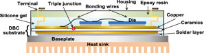
Figure 4. Typical power module packaging structure.
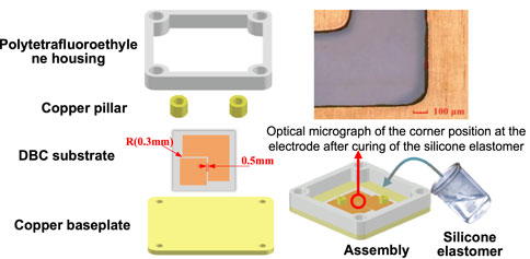
Figure 5. Main components of power module package insulation specimen.
In order to explore the reliability of package insulation under square electrothermal coupling stress and collect optical signals of each band of PD in real-time, a mul-ti-spectral synchronous detection system was built, as shown in Figure 6.
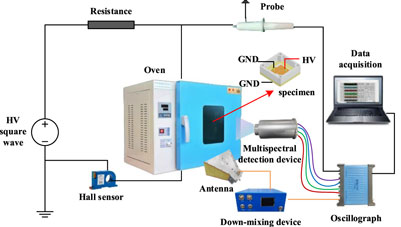
Figure 6. Multi-spectral simultaneous detection system for PD.
The output voltage magnitude of the unipolar high-voltage square pulse power supply used in the experiment is 0∼15 kV, the maximum repetition frequency is 10 kHz, and the shortest rise time is 50 ns. The experiment is carried out in a dark room to reduce the interference of ambient light so that it does not affect the PD light measurement. The system wiring method is shown in Figure 6. The unipolar square pulse high-voltage power supply is introduced into the constant temperature oven, and the packaged specimen is placed in the constant temperature oven to control the experimental temperature to be constant. The high-voltage differential probe measures the voltage at both ends of the specimen in real time. The broadband horn antenna and the mul-ti-spectral sensor are facing the surface of the PD specimen, and the distance is fixed at 15 cm. The oscilloscope is a portable 8-channel acquisition card. The acquisition software is driven by the LabVIEW program, which can realize multi-channel simultaneous display and acquisition. According to the actual operating conditions of the power module, the package insulation PD experiment is set as follows: the applied voltage type is a uni-polar square pulse, with a rise time of 400 ns, a frequency of 5 kHz, and a duty cycle of 50%. To achieve the effect of accelerated aging by square wave electrothermal combination, and taking into account the suitable temperature range of package insulation, the experimental temperatures in this paper are set to 120°C, 150°C, and 180°C respectively, and the changes of partial discharge multispectral signal characteristics at different temperatures are investigated.
The typical down-mixing and multi-spectral PD signal waveforms are shown in Figure 7. It can be seen from the figure that the down-mixing signal and multi-spectral signal of PD have good synchronization. There is slight conducted electromagnetic interference in the optical signal waveform, but the magnitude of the PD signal is much larger than the conducted interference.
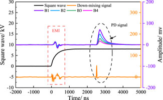
Figure 7. Typical down-mixing and multispectral optical PD signals.
In the PDIV experiment, in order to ensure the accuracy and reliability of the experiment, five groups of specimens from the same batch were set under the same experimental conditions, and the test was carried out after the temperature in the constant temperature oven reached the set value and stabilized. The dV/dt and square pulse width of the square pulse was fixed at 16 V/ns and 100 μs respectively. According to the IEC60270 recommendation (Zhong et al., 2022), during the PDIV test, a lower voltage must be applied to the specimen and gradually increased until the first PD occurs. Therefore, a step of 100 V per second staircase-increasing procedure was used in the experiment, and each group of experiments was repeated 5 times. The arithmetic mean of the five groups of experimental data was taken as the final result for data analysis. The change pattern is shown in Figure 8.
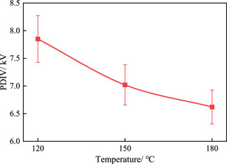
Figure 8. PDIVs under different temperatures.
As the temperature increases from 120°C to 180°C, the PDIV gradually decreases from 7.8 kV to 6.6 kV and the average error gradually decreases, indicating that the increase in temperature significantly reduces the PD initiation voltage of the insulating material. The decrease in PDIV may be the result of the combined action of various mechanisms (Wang et al., 2014; Zang et al., 2024). The silicon elastomer encapsulated insulation is a multi-dielectric composite material, and the thermal expansion coefficient of different materials is different. At higher temperatures, micro-defects are easily formed at the triple junction point, resulting in electric field distortion. At the same time, high temperature will destroy the chemical structure of the molecule, promote the degree of crosslinking, and further reduce its insulating properties. In addition, this paper also extracts the average intensity of PD multispectral signals when the square wave voltage is fixed to PDIV at three temperatures, and the results are shown in Table 2.
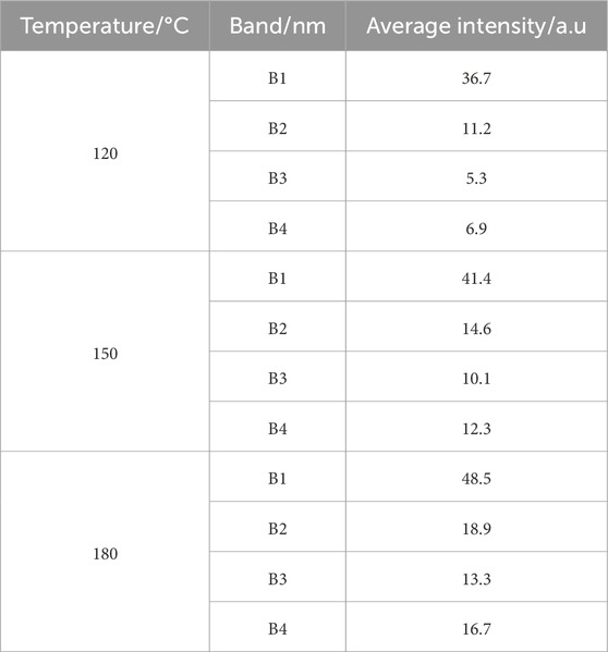
Table 2. The average intensity of PD multispectral signals under different temperatures.
From the data analytics in Table 2, it can be obtained that the radiation intensities of all bands of the PD multispectral signal increase with temperature, but the increase is significant. From 120°C to 180°C, the average intensity of the B1 band increases by 32.2%, the average intensity of the B2 band increases by 68.8%, and the spectral intensity of the short-wave range increases more slowly; the average intensity of the B3 band increases by 151%, the average intensity of the B4 band increases by 142%, and the spectral intensity of the long-wave range increases sharply, indicating that the center of gravity of the spectral radiation gradually shifts to the long-wave direction with the increase of temperature.
The increase in the average light intensity of B1 and B2 may be related to the intensification of high-energy discharge activity. The increase in temperature will lead to an increase in the conductivity of silicon elastomers, an increase in leakage current, and an increase in local electric field distortion, which will lead to more frequent high-energy electron avalanches, enhanced near-ultraviolet light radiation, and high-temperature aging will also produce defects (Cao et al., 2024), releasing short-wave photons during the carrier recombination process. The significant increase in the average light intensity of B3 and B4 is dominated by thermal aging and material degradation (Shang et al., 2024). High temperature accelerates the movement of molecular chains, resulting in increased vibration of C-H and Si-O bonds in the silicon elastomer molecular chains, releasing a large number of photons in the near-infrared band. The sharp growth of the B3 and B4 bands can serve as an early sign of insulation aging at high temperatures.
According to the requirements of IEC 61278, the magnitude of the applied voltage should be higher than the PDIV of the corresponding applied voltage type to ensure that PD can occur repeatedly. Based on the previous experimental results, the magnitude of the applied voltage is fixed at 8.5 kV for the characteristic experiment, and the computer collects five cycles of data every 5 s.
The PD radiation spectrum of silicone elastomer package insulation provides physical information in the microscopic dimension. The light intensity at a specific wavelength is usually determined by the light radiation path and the defect structure (Zang et al., 2019; Yu and Zhang, 2024). Therefore, the PD multi-spectral characteristics can more intuitively reflect the insu-location state of the package. In this paper, the effect of temperature on the statistical characteristics of PD is studied by selecting the average optical signal intensity, the maximum optical signal intensity, and the cumulative optical signal intensity. The results are shown in Figures 9–11. Here, the average optical signal strength represents the average amplitude of the signals in each band over 60 cycles per minute, the maximum optical signal strength represents the average maximum amplitude of the signals in each band over 60 cycles per minute, and the cumulative optical signal strength represents the sum of all signal amplitudes in each band over 60 cycles per minute.
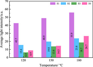
Figure 9. Variation of average light intensity of PD under different temperatures.
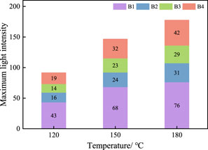
Figure 10. Variation of maximum light intensity of PD under different temperatures.
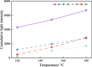
Figure 11. Variation of cumulative light intensity of PD under different temperatures.
The statistical results of the average light intensity in Figure 9 show that from 120°C to 180°C, the average light intensity in the B1 to B4 bands increases by 1.3 times, 1.5 times, 2.9 times, and 3 times, respectively. Among them, the average light intensity in the B1 band is dominant at different temperatures, but the average light intensity in B3 and B4 increases significantly with the increase of temperature, and the effect of temperature increase on photon excitation in the B3 and B4 bands is more prominent.
As the temperature rises, the maximum intensity and cumulative intensity of the PD increase, and the multi-spectral signal performance is different. Among them, the B1 band performs outstandingly and always dominates, and the B4 band has an obvious growth trend in Figures 9, 10. Silicone elastomer encapsulation insulation may break or degrade its molecular chain at high temperatures, producing free radicals or small molecule fragments (Zhou et al., 2023). These degradation products may have higher energy, resulting in strong radiation in the near-ultraviolet band. As the temperature rises, the PD will produce more high-energy electrons and ions, and excite molecules or surrounding gas molecules, resulting in an increase in photon emission in the ultraviolet band. At the same time, the newly generated free radicals or small molecule fragments will also introduce different vibration modes (Wang et al., 2024a), resulting in an increase in radiation photons in the near-infrared band.
In this paper, the change of insulation aging life and discharge times with temperature and the change of discharge times with temperature in each band are counted. The results are shown in Figures 12, 13. In this paper, the complete cycle of insulation breakdown is taken as the aging life, and the average value of the detection results of the same batch of samples is taken. The number of discharges represents the average number of optical signals generated by the partial amplifier detected in all cycles per minute. Previous experiments have proved that the spectral signals of each band of the partial amplifier are synchronized, so when the number of discharges is counted in a single cycle, if there is an optical signal in any of the four bands, it can be regarded as a discharge.
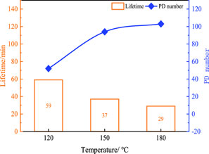
Figure 12. Variation of insulation lifetime and PD number under different temperatures.
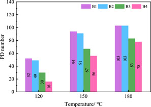
Figure 13. Variation of PD number in each band under different temperatures.
From 120°C to 180°C, with the increase of temperature, the average life of the power module package insulation decreases by nearly 50%, while the number of discharges increases by about 2 times. The higher the temperature, the higher the probability of electronic collision inside the insulation increases (Gao et al., 2024), and the development of aging defects is exacerbated, so that the performance of the partial discharge is more obvious, and the number of optical signals shows an increasing trend. The high temperature will exacerbate the process of the partial discharge and lead to the shortening of the life of the package insulation (Wang et al., 2024b). The statistical results of the number of discharges in Figure 13 show that with the increase of temperature, the number of discharges in the B1∼ B4 band increases by 2 times, 2.1 times, 2.8 times, and 4.9 times, respectively.
Since the applied positive polarity repeating square wave frequency is 5 kHz, a complete square wave cycle time is 200 μs. For ease of description, the phase of the square pulse is expressed as the percentage of one cycle (0%–100%), and the initial rising position of the square pulse is defined as 0. Under the same test conditions, 500 square wave cycle data were selected for each group of temperatures. The number of discharges and their phase distributions are shown in Figure 14.
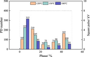
Figure 14. Variation of PD number and phase under different temperatures.
At 120°C, the discharge activity mainly occurs between 10% −20% and 40%–50%. With the increase of temperature, the number of discharges increases, and the discharges are concentrated on the rising edge (0%–10%) and the falling edge (50%–60%) of the square wave. When the temperature increases to 180°C, the probability of discharge activity occurring between 0%–10% and 50%–60% is as high as 90%, indicating that the discharge activity at high temperature has obvious phase concentration, and the number of discharges at the rising edge of the square wave is significantly more than the falling edge of the square wave.
In the edge region on both sides of the square wave, the rapid change of the electric field leads to slow charge accumulation, and the partial discharge mostly occurs in the high-level region, and the discharge activity is obvious in the 10%–20% phase range at 120°C. With the increase of temperature, the carrier mobility accelerates, the kinetic energy obtained by electrons in the electric field increases, and the probability of collision ionization increases exponentially, resulting in an increase in the number of discharges in a single cycle; at the same time, the charge flow rate accelerates, making it easier for the accumulated charge to break through the threshold, and the partial discharge activity rises and falls to the square wave.
Under the square wave electrothermal coupling stress, the failure of the power module package insulation usually originates from the triple junction (such as the junction of silicon elastomer-ceramic substrate-copper electrode). The rapid breaking of the square wave voltage will lead to a transient high electric field, and there are differences in the dielectric constant and conductivity of different materials at the triple junction, and the electric field distribution will be distorted here. At the same time, the thermal stress caused by temperature changes may exacerbate the microstructural changes at the material interface and accelerate the aging of the material to form a discharge channel. Due to the concentration of electrical and thermal stresses in this area, partial discharges are more likely to be triggered here (Chen, et al., 2024). Figure 15 shows a schematic diagram of partial discharges at the three junction points at high temperatures and square wave voltages.
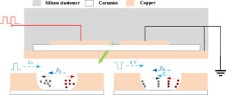
Figure 15. Schematic diagram of PD at triple junction point.
Studies have shown that the contribution of square wave electrical stress to partial discharge is the main component, and thermal stress is more to accelerate the aging process (Sili et al., 2013). The rapidly rising edge of a high dV/dt positive square wave leads to a transient electric field enhancement, which drives electrons to inject from the copper electrode, and the silicon elastomer molecules are dissociated by high field strength to produce free electrons and positive ions. In the high-level stage of the square wave, the positive ions move along the direction of the applied electric field Ein, partially recombine with the electrons during the movement, and the electrons move in the opposite direction of the electric field, which may be trapped by the electrodes or accumulated at the interface. The residual charge forms an additional electric field Eq in the opposite direction and weakens the applied electric field Ein. When the combined field strength of Ein and Eq still exceeds the critical field strength, a positive discharge occurs (square wave rising edge region). At this stage, the high-energy particles have a high initial kinetic energy and carry enough energy to transition. The radiation photons are mainly in the near-ultraviolet band (Zhang and He, 2017). The driving force of charge migration in the low-level stage temporarily disappears, and the remaining unneutralized charge (such as electrons or ions trapped by traps) is driven by the additional field strength Eq to continue to diffuse or slowly migrate and form a built-in field strength Ei. When the superimposed field strength exceeds the critical field strength, it will trigger reverse discharge (square wave falling edge region). The energy of the particles in this stage is insufficient and can only transition between low energy levels. The radiation photons are mainly in the visible and near-infrared bands.
When the polarity of the square wave is switched, because the dielectric relaxation time of the silicon elastomer is greater than the duration of the high level, the charge can hardly be dissipated in each cycle. At the same time, the high temperature reduces the activation energy of the trap, causing the charge in the deep trap to be released, resulting in the continuous accumulation of space charges inside the material. The accumulated space charge will form a new additional electric field inside the material and superimpose with the applied electric field, resulting in the local field strength exceeding the material breakdown field strength, triggering a partial discharge (Jiang et al., 2024), and the plasma generated by the discharge will further damage the material and form more defects. The new defect causes the electric field to further concentrate, forming more discharge channels, and this process accelerates at high temperatures, increasing the number of PD in a single cycle.
In addition, the experimental results in the third section above show that in all bands from B1 to B4, the optical radiation intensity and discharge times in the B1 band dominate, while the increase in the optical radiation intensity and discharge times in the B4 band is the most prominent. Studies have shown that during partial discharge, high-energy particles such as electrons or ions collide with molecules, causing the particles to be excited to a high-energy state. When they return to a low-energy state, a transition occurs. These transitions release photons with higher energy and shorter wavelengths (Zhao et al., 2020). Therefore, the intensity of near-ultraviolet (B1) light radiation is closely related to the energy in the discharge, which can reflect the intensity of the discharge. While near-infrared spectroscopy is usually related to molecular vibration energy levels, insulating materials undergo molecular structural changes during aging (such as the stretching vibration of C-H bonds or the bending vibration of Si-CH3), increasing the activity of certain vibration modes (Cai et al., 2010), thereby enhancing near-infrared radiation. Therefore, the enhancement of near-infrared (B4) light radiation can reflect changes in the internal chemical structure of the material, that is, the deepening of aging.
1) This paper introduces a PD multi-spectral optical sensing method based on SiPM, which features high sensitivity and strong anti-interference capabilities. Aiming at the physical phenomenon of PD light radiation from power module packaging insulation across different spectral bands, a PD multi-spectral synchronous detection platform was established, and accelerated aging experiments were conducted under square pulse voltages.
2) Compared with the PD detection results of the down-mixing method, the PD detection effect of the multi-spectral sensing device is good, and the corresponding optical signals of each band are synchronized. The comparison results of PDIV show that as the temperature increases, PDIV decreases, and the intensity of PD radiation light signals increases. High temperatures will reduce the performance of packaging insulation materials and intensify photon excitation activity.
3) The effects of temperature on the characteristics of PD light intensity, lifetime, and PD number are studied. The results show that the multispectral statistical characteristics of PD are different under high temperatures, and the average light intensity, maximum light intensity, and cumulative light intensity of each band increase with the increase of temperature. The optical signal in the near-ultraviolet band is the largest under all conditions, and the optical signal in the near-infrared band shows a significant increasing trend with rising temperature. The lifetime of the power module package insulation decreases with the increase of temperature, and the PD number in each band increases. In addition, the discharge activity gradually concentrates on both sides of the square pulse with the increase of temperature.
The original contributions presented in the study are included in the article/supplementary material, further inquiries can be directed to the corresponding author.
QH: Writing–review and editing. QN: Writing–review and editing. BW: Writing–review and editing. YiD: Writing–original draft, Writing–review and editing. MS: Writing–review and editing. YaD: Writing–review and editing.
The author(s) declare that financial support was received for the research and/or publication of this article. The funder was not involved in the study design, collection, analysis, interpretation of data, the writing of this article, or the decision to submit it for publication.
Authors QH, QN, MS, and YaD were employed by State Grid Shanghai Extra High Voltage Company.
The remaining authors declare that the research was conducted in the absence of any commercial or financial relationships that could be construed as a potential conflict of interest.
The authors declare that no Generative AI was used in the creation of this manuscript.
All claims expressed in this article are solely those of the authors and do not necessarily represent those of their affiliated organizations, or those of the publisher, the editors and the reviewers. Any product that may be evaluated in this article, or claim that may be made by its manufacturer, is not guaranteed or endorsed by the publisher.
Auge, J. L., Lesaint, O., and Thi, A. T. V. (2013). “Optical measurement of partial discharges under impulse voltage on ceramic substrates embedded in silicone oil,” Report Conference on Electrical Insulation and Dielectric Phenomena. IEEE
Cai, D., Neyer, A., Kuckuk, R., and Heise, H. M. (2010). Raman, mid-infrared, near-infrared and ultraviolet–visible spectroscopy of PDMS silicone rubber for characterization of polymer optical waveguide materials. J. Mol. Struct. 976, 274–281. doi:10.1016/j.molstruc.2010.03.054
Cao, H., Zhou, C., Meng, Y., Shen, J., and Xie, X. (2024). Advancement in transformer fault diagnosis technology. Front. Energy Res. 12, 1437614. doi:10.3389/fenrg.2024.1437614
Chen, M., Wang, Y., Ding, Y., Fan, L., and Yin, Y. (2024). Self-adaptive field-grading coating for partial discharge mitigation of high voltage power module under high dv/dt square wave voltage. IEEE Trans. Power Electron. 39, 9079–9083. doi:10.1109/tpel.2024.3390672
Ding, Y., Wang, Y., Sun, H., and Yin, Y. (2023). High-temperature partial discharge characteristics of power module packaging insulation under square pulse with high dv/dt based on down-mixing method. IEEE Trans. Ind. Electron. 70, 7334–7342. doi:10.1109/TIE.2022.3201276
Fabian, J. H., Hartmann, S., and Hamidi, A. (2005). “Analysis of insulation failure modes in high power IGBT modules,” in Fourtieth IAS Annual Meeting. Conference Record of the 2005 Industry Applications Conference, 2005, Hong Kong, China, 02-06 October 2005, 799–805.
Gao, T., He, D., Xu, Z., Wei, J., Xie, S., Teyssède, G., et al. (2024). Degradation induced by charge relaxation in silicone gels under the ultra-fast pulsed electric field. High. Volt. 9, 1383–1392. doi:10.1049/hve2.12484
Hou, F., Wang, W., Cao, L., Li, J., Su, M., Lin, T., et al. (2020). Review of packaging schemes for power module. IEEE J. Emerg. Sel. Top. Power Electron. 8, 223–238. doi:10.1109/JESTPE.2019.2947645
Jiang, J., Cui, D., Liu, J., Chen, B., Chen, J., and Fu, R. (2024). Partial discharge characteristics of epoxy resin under high-frequency pulse electrical stress. IEEE Trans. Power Electron. 40, 2017–2027. doi:10.1109/TPEL.2024.3421624
Mancinelli, P., Cavallini, A., Chalashkanov, N., Dodd, S. J., and Dissado, L. A. (2016). “Electrical treeing in silicone gel under square voltage: frequency, rise time and crosslinking influence,” in 2016 IEEE Conference on Electrical Insulation and Dielectric Phenomena, Toronto, ON, Canada, 16-19 October 2016, 979–982. doi:10.1109/ceidp.2016.7785537
Ren, M., Dong, M., and Liu, J. (2016). Statistical analysis of partial discharges in SF6 gas via optical detection in various spectral ranges. Energies 9, 152. doi:10.3390/en9030152
Ren, M., Zhang, C., Dong, M., and He, Z. (2020). Fault prediction of gas-insulated system with hypersensitive optical monitoring and spectral information. Int. J. Electr. Power Energy Syst. 119, 105945. doi:10.1016/j.ijepes.2020.105945
Ren, M., Zhou, J., Yang, S., Zhuang, T., Dong, M., and Albarracín, R. (2018). Optical partial discharge diagnosis in SF6 gas-insulated system with SiPM-based sensor array. IEEE Sens. J. 18, 5532–5540. doi:10.1109/JSEN.2018.2836423
Shang, X., Pang, L., Bu, Q., Wu, Z., and Zhang, Q. (2024). Partial discharge behaviors excited by high-frequency square pulse voltage in cast resin insulation with thermal-induced defect. IEEE Trans. Dielectr. Electr. Insul. 31, 40–49. doi:10.1109/TDEI.2023.3343325
Sili, E., Cambronne, J. P., Naude, N., and Khazaka, R. (2013). Polyimide lifetime under partial discharge aging: effects of temperature, pressure and humidity. IEEE Trans. Dielectr. Electr. Insulation 20, 435–442. doi:10.1109/tdei.2013.6508745
Siow, K. S., Chen, T. F., Chan, Y. W., Jalar, A., Vemal, R. M., Chua, S. T., et al. (2015). “Characterization of silicone gel properties for high power IGBT modules and MEMS,” in 2015 IEEE Conference on Sustainable Utilization And Development In Engineering and Technology (CSUDET), Selangor, Malaysia, 15-17 October 2015, 1–5. doi:10.1109/csudet.2015.7446220
Wang, J., Wu, W., Song, Y., Wang, W., Ren, H., and Li, Q. (2024). Gas-generation mechanism of silicone gel in high-temperature thermal decomposition for high-voltage and high-power device encapsulation. IEEE Trans. Dielectr. Electr. Insul. 31, 2830–2839. doi:10.1109/TDEI.2024.3352536
Wang, J., Yan, H., Chen, C., Wang, W., and Li, Q. (2024). Evolutionary mechanism and damage characteristics of “gel–solid” creeping discharge of power device package insulation under coupled temperature–frequency effects. IEEE Trans. Dielectr. Electr. Insul. 31, 577–586. doi:10.1109/TDEI.2023.3302273
Wang, P., Cavallini, A., and Montanari, G. C. (2014). The influence of repetitive square wave voltage parameters on enameled wire endurance. IEEE Trans. Dielectr. Electr. Insul. 21, 1276–1284. doi:10.1109/TDEI.2014.6832275
Wang, Y., Ding, Y., Yuan, Z., Peng, H., Wu, J., Yin, Y., et al. (2021). Space-charge accumulation and its impact on high-voltage power module partial discharge under DC and PWM waves: testing and modeling. IEEE Trans. Power Electron. 36, 11097–11108. doi:10.1109/TPEL.2021.3072655
Wang, Y., Wu, J., and Yin, Y. (2022). Space charge and trap in high-voltage power module packaging insulation: simultaneous measurement and 2-D simulation. IEEE Trans. Dielectr. Electr. Insul. 29, 1400–1408. doi:10.1109/TDEI.2022.3183677
You, H., Wei, Z., Hu, B., Zhao, Z., Na, R., and Wang, J. (2021). Partial discharge behaviors in power modules under square pulses with ultrafast dv/dt. IEEE Trans. Power Electron. 36, 2611–2620. doi:10.1109/TPEL.2020.3014043
Yu, R., and Zhang, Z. (2024). Transformer partial discharge location technology based on gradient oil temperature. Front. Energy Res. 12, 1428012. doi:10.3389/fenrg.2024.1428012
Zang, Y., Niasar, M. G., Xu, Y., Li, Z., Qian, Q., Jiang, X., et al. (2024). Optical detection and characteristics of PCB partial discharge in more-electric aircraft under square wave voltage. IEEE J. Emerg. Sel. Top. Power Electron. 12, 5558–5567. doi:10.1109/JESTPE.2024.3371010
Zang, Y., Qian, Y., Liu, W., Xu, Y., Sheng, G., and Jiang, X. (2019). A novel partial discharge detection method based on the photoelectric fusion pattern in GIL. Energies 12, 4120. doi:10.3390/en12214120
Zhang, C., Xu, Y., Dong, M., Burgos, R., Ren, M., and Boroyevich, D. (2020). Design and assessment of external insulation for critical components in a medium voltage SiC-based converter via optical method. IEEE Trans. Power Electron. 35, 12887–12897. doi:10.1109/TPEL.2020.2996262
Zhang, S., and He, J. (2017). Light emission characteristics during the initiation of the electric tree in insulating polymers. J. Eng. 2017, 2650–2654. doi:10.1049/joe.2017.0837
Zhao, Y., Li, Y., Li, K., Han, D., Qiu, Z., and Zhang, G. (2020). Emission spectrum analysis of two typical partial discharge forms under high-frequency square wave voltages. IEEE Access 8, 219946–219954. doi:10.1109/ACCESS.2020.3034458
Zhong, X., Arachchige, T. G., Ma, H., Ekanayake, C., and Saha, T. K. (2022). Experimental study on partial discharge inception voltage of pressboard-enclosed void at different frequencies from the perspective of the first partial discharge time lag. IEEE Trans. Dielectr. Electr. Insul. 29, 1382–1391. doi:10.1109/TDEI.2022.3183674
Keywords: square pulse, power module package insulation, partial discharge, temperature, multi-spectrum
Citation: Heng Q, Ni Q, Wang B, Ding Y, Sun M and Ding Y (2025) High-temperature partial discharge characteristics of power module packaging insulation under square pulses based on multispectral optical detection method. Front. Energy Res. 13:1580823. doi: 10.3389/fenrg.2025.1580823
Received: 21 February 2025; Accepted: 19 March 2025;
Published: 02 April 2025.
Edited by:
Feng Liu, Nanjing Tech University, ChinaReviewed by:
Hongtu Cheng, Nanjing Tech University, ChinaCopyright © 2025 Heng, Ni, Wang, Ding, Sun and Ding. This is an open-access article distributed under the terms of the Creative Commons Attribution License (CC BY). The use, distribution or reproduction in other forums is permitted, provided the original author(s) and the copyright owner(s) are credited and that the original publication in this journal is cited, in accordance with accepted academic practice. No use, distribution or reproduction is permitted which does not comply with these terms.
*Correspondence: Yi Ding, eWlkaW5nc2p0dUAxNjMuY29t
Disclaimer: All claims expressed in this article are solely those of the authors and do not necessarily represent those of their affiliated organizations, or those of the publisher, the editors and the reviewers. Any product that may be evaluated in this article or claim that may be made by its manufacturer is not guaranteed or endorsed by the publisher.
Research integrity at Frontiers
Learn more about the work of our research integrity team to safeguard the quality of each article we publish.