 Jinliang Li1,2
 Zhengmei Lu
 Guo Xu
- 1State Grid Hunan Electric Power Company Limited Research Institute, Changsha, China
- 2State Grid Joint Laboratory for Intelligent Application and Key Equipment in Distribution Network Institute, Changsha, China
- 3School of Automation, Central South University, Changsha, China
A modified two-stage buck-DAB (MBDAB) converter is proposed to improve the performance of the traditional two-stage buck-DAB (TSBDAB) converter. In the MBDAB converter, the DAB can work with fixed voltage gain and voltage-matched condition under a wide input voltage range. The voltage gain of the converter is adjusted through the added front-end stage, which is similar to a buck converter. Compared with the TSBDAB converter, only part of the transmitted power flows through the front-end stage, so the loss of the buck stage and the burden of zero-voltage switching (ZVS) can be reduced. Detailed analysis of the working principle, partial power characteristics, and the full-load ZVS range design are presented. To verify the effectiveness of the proposed MBDAB converter, experimental results are obtained from a prototype with a rated power of 1 kW.
1 Introduction
Bidirectional DC/DC converters play a crucial role in various applications like DC microgrids and energy storage systems to provide electrical isolation and voltage gain regulation capability (Inoue and Akagi, 2007; Masrur et al., 2018; Tu et al., 2019). In the domain of traditional IBDC converters, there are two key types: resonant converters and dual active bridge (DAB) converters (Zhao et al., 2014). DAB converters have gained significant interest due to their numerous benefits, such as electrical isolation, high efficiency, the ability to transfer energy bidirectionally, and soft-switching characteristics (Shao et al., 2019).
The single phase shift (SPS) control has only one degree of freedom, which is very simple (Doncker et al., 1988). However, the efficiency of the SPS-controlled DAB converter is low when the voltage gain is far away from the unity gain due to the large current stress and backflow power, and the zero-voltage switching (ZVS) cannot be achieved under full range. Therefore, to improve the efficiency of the DAB converter under a wide voltage range, modulation strategies with more control variables have been proposed. Extended phase shift (EPS) control and dual phase shift (DPS) control are two common two-degree-of-freedom control methods (Zhao et al., 2012; Sun et al., 2020). An inner phase-shift angle is introduced to reduce the RMS inductance current and the backflow power under a wide voltage range. Triple phase shift (TPS) control (Everts, 2017; Guo, 2020) is designed to further improve the performance of the DAB. There are three degrees of freedom in TPS control, which results in increased complexity in both the operation modes and control strategy due to the added degree of freedom.
Another effective and simple solution for improving the performance of the converter under a wide voltage range is the restructuring of its topology (Alou et al., 2001; Lee et al., 2011; Fu et al., 2020; Xu et al., 2020; Liao et al., 2022; Lin et al., 2022). The core concept of this technique is to enable the DAB converter to operate under a unity gain condition across a wide voltage range by restructuring the topology. One straightforward way is the two-stage cascade solution. To achieve high performance, the IBDC converter operates under fixed voltage gain in the two-stage cascade scheme. The two-stage structure includes two DC/DC converters, and one of them has isolation properties, as detailed in Alou et al. (2001), Lee et al. (2011), Fu et al. (2020), and Xu et al. (2020). Figure 1 illustrates the configuration of the TSBDAB converter. Fu et al. (2020) enhanced the efficiency by combining the IBDC converter with a non-isolated boost converter. ZVS of all switches is achieved, and the overall losses are reduced. Xu et al. (2020) combined a DAB converter and a buck–boost converter to achieve superior performance under a wide voltage gain range. Lin et al. (2022) described the combination of the DAB and the boost converter in input-series configuration. High efficiency can be achieved by power-sharing adjustments between the two converters.
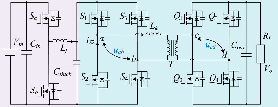
Figure 1. Topology of the TSBDAB converter.
All of the power should be transferred by the front-end stage in the existing two-stage scheme, which leads to increased conversion loss. To improve the efficiency of the two-stage scheme and reduce the front-end-stage-transferred power, a partial power converter (PPC) approach as mentioned in Sun et al. (2008), Zientarski et al. (2019), and Liao et al. (2022) can be used. The PPC concept involves integrating the PPC submodule alongside the main power converters, either in parallel or in series. It is important to note that the PPC solution typically does not provide electrical isolation, as it often uses buck or buck/boost converters for the DC–DC conversion with partial power characteristics, as explained in Sun et al. (2008).
In this article, a modified isolated bidirectional buck-DAB converter is proposed to construct partial power transmission characteristics of the front-stage converter and further improve the efficiency of the two-stage converter under a wide voltage range. The proposed converter only requires a simple change in the connection architecture of the TSBDAB converter. In the MBDAB converter, when the input voltage changes, the front-end buck stage performs a gain adjustment, whereas DAB operates under a fixed voltage gain condition. In addition, the buck stage can only transmit part of the output power, which is due to the change in the connection architecture of the TSBDAB scheme. All the switches of the proposed converter can achieve the ZVS operation.
2 Proposed MBDAB converter and operation principles
2.1 Proposed modified buck-DAB converter
Figure 2 illustrates the proposed MBDAB converter. Compared with the TSBDAB converter in Figure 1, to achieve the partial power conversion, the source of S1 is disconnected from the source of S3, and the source of S3 is directly connected to the input voltage. In addition, a blocking capacitor Cb is added to ensure that the voltages on both sides of the leakage inductor Lk are matched. The buck stage consists of two switches (Sa-b), an inductor (Lf), and a capacitor (CBuck). The DAB stage consists of two full bridges in the primary side and the secondary side, connected by a high-frequency transformer T with the turns ratio of Np:1, an inductor (Lk), and a capacitor (Cb).
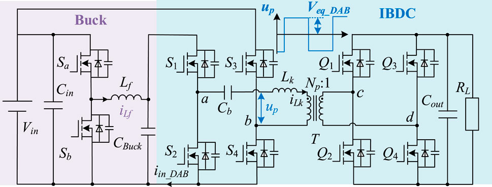
Figure 2. Topology of the proposed MBDAB converter.
2.2 Mechanism of DC block capacitor Cb
The equivalent circuit of the DAB stage is shown in Figure 3. When the DAB stage is under the SPS control, the voltages on both sides of the leakage inductor are in volt–second equilibrium, which ensures that the inductor current iLk does not diverge. According to Figure 3, the relationship can be calculated as Eq. 1:
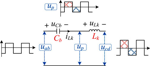
Figure 3. Equivalent circuit.
The steady state of the converter means that the average voltage of inductor Lk is 0. The relationship between the uab, up and ucd is shown in Figure 3, the average values of ucd and uab are 0 and (Vin−VBuck)/2, then the voltage on DC block capacitor Cb can be deduced as Eq. 2:
2.3 Modulation strategies and operation principles
Figure 4 illustrates the modulation strategy and theoretical operating waveforms of the proposed MBDAB converter. According to Figure 4, switches Sa and Sb are driven complementarily, and pulse width modulation is applied to the buck converter. As for the DAB stage, the conventional SPS modulation is applied. It is very simple with a fixed 50% duty ratio.
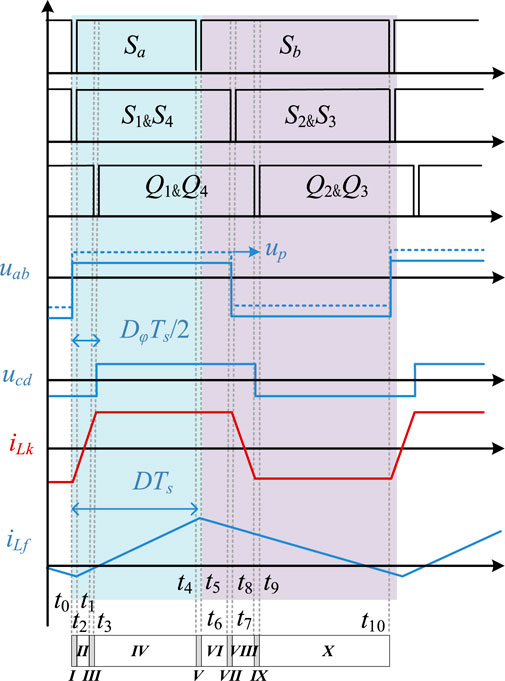
Figure 4. Key waveforms of the MBDAB converter.
The duty cycle D of Sa is to regulate the voltage across CBuck. The half-cycle phase shift ratio Dφ is used to regulate the output power of DAB. It is worth pointing out that Sa and S1 do not have to be turned on at the same time.
The 10 operating intervals are analyzed as follows and shown in Figure 5.
Stage I (t0–t1): At t0, switches Sb, S2, and S3 are turned off. During stage I, since the currents iLf and iLk are negative, respectively, the body diodes of Sa, S1, and S4 are turned on. The conduction of diodes provides the conditions for the ZVS of the corresponding switches.
Stage II (t1–t2): At t1, switches Sa, S1, and S4 are turned on under the ZVS condition. The voltage across inductors Lf and Lk is kept constant, and the currents iLf and iLk increase linearly. The inductor currents iLf and iLk are expressed in Eqs 3, 4:
Stage III (t2–t3): At t2, switches Q2 and Q3 are turned off. During stage III, since the current iLk is positive, the body diodes of Q1 and Q4 are turned on. The conduction of diodes provides the conditions for the ZVS of the corresponding switches.
Stage IV (t3–t4): At t3, switches Q1 and Q4 are turned on under the ZVS condition. Since the voltage across the inductor Lk is zero under the voltage-matching condition, iLk keeps constant.
Stage V (t4–t5): At t4, the switch Sa is turned off. Since the inductor current iLf is positive during stage V, the body diodes of Sb are turned on, which provides the conditions for ZVS of Sb.
Stage VI (t5–t6): At t5, the switch Sb is turned on under the ZVS condition. The voltage across the inductor Lf is kept constant, and the current iLf decreases linearly which is expressed in Eq. 5:
Stage VIII (t7–t8): At t7, switches S2 and S3 are turned on under the ZVS condition. The voltage across the inductor Lk is kept constant, and the current iLk decreases linearly, which is expressed in Eq. 6:
Stage IX (t8–t9): At t8, switches Q1 and Q4 are turned off. During stage IX, since the current iLk is negative, the body diodes of Q2 and Q3 are turned on. The conduction of diodes provides the conditions for the ZVS of the corresponding switches.
Stage X (t9–t10): At t9, switches Q2 and Q3 are turned on under the ZVS condition. Since the voltage across the inductor Lk is zero under the voltage-matching condition, the current iLk keeps constant.
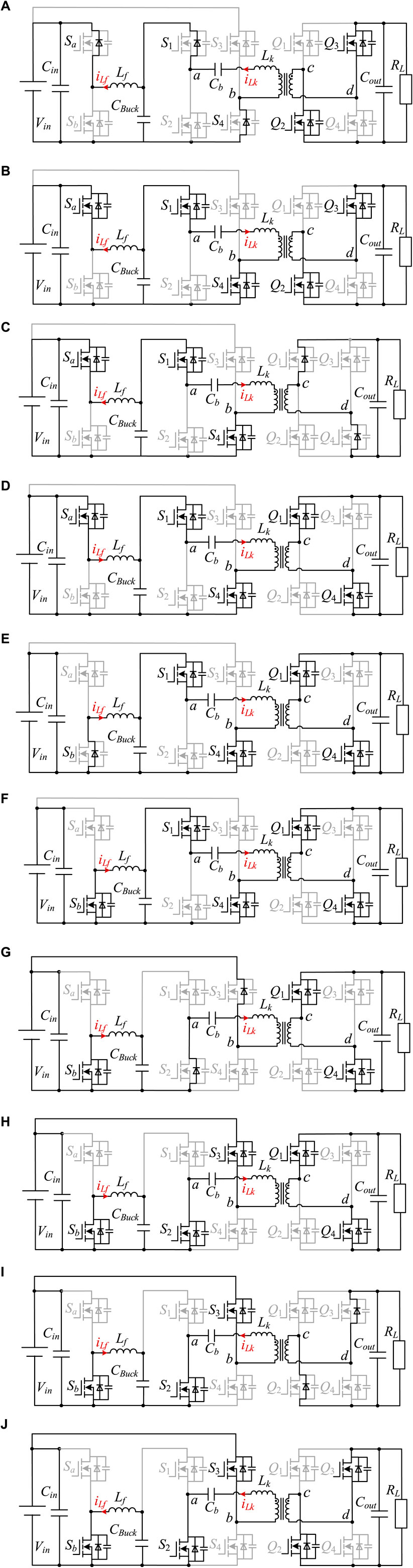
Figure 5. Operational principles of the proposed converter: (A) stage I (t0–t1); (B) stage II (t1–t2); (C) stage III (t2–t3); (D) stage IV (t3–t4); (E) stage V (t4–t5); (F) stage VI (t5–t6); (G) stage VII (t6–t7); (H) stage VIII (t7–t8); (I) stage IX (t8–t9); and (J) stage X (t9–t10).
3 Steady-state analysis of the proposed MBDAB converter
3.1 Analysis of the voltage gain ratio of the MBDAB converter
Under the SPS modulation strategy, the output power of DAB in the MBDAB converter can be expressed as Eq. 7:
where Np is the ratio of the high-frequency transformer and fs is the switching frequency of the converter. Veq is one half of the peak-to-peak value of the voltage up, which can also be regarded as the equivalent input voltage of DAB. The expression of Veq can be deduced as Eq. 8:
Therefore, the voltage gain of the DAB circuit in the modified buck-DAB converter can be derived as follows:
where RL is the resistance value of the load resistance and M1 is the voltage gain of the DAB circuit. In order to achieve the voltage-matched condition of the DAB primary and secondary sides, the normalized gain of DAB is controlled to be constant at 1 in this converter, that is, NpM1 = 1.
The voltage gain of the buck circuit is expressed as Eq. 10:
Considering the voltage gain of the buck part yields Eq. 11:
The voltage gain of the MBDAB converter can be expressed as Eq. 12:
It can be known from Eq. 9 that the voltage gain ratio is related to D of the buck stage and Np. When D is within the range of [0,1], the normalized voltage gain ratio (MNp) is within the range of [0.5,1].
3.2 Transferred power of the buck stage
In the proposed MBDAB converter, the buck stage only transfers power when S1 is on, so the transferred power of it is always smaller than the output power of the system. In addition, the power is directly transferred from the input voltage Vin when the switch S3 is on. Then, the inductor current of the buck stage has a smaller offset and RMS value. It will reduce the loss and size of the buck inductor and help meet the ZVS condition of the buck switches.
The power of the MBDAB converter can be expressed as Eq. 13, according to power transmission characteristics of the DAB stage.
Because the average inductor current is equal to half of the average DAB stage input current, the load current of the buck circuit can be expressed as Eq. 14:
The transferred power of the buck stage can be expressed as Eq. 15:
The power transfer ratio for the buck stage to the DAB stage can be expressed as Eq. 16:
3.3 Analysis of the ZVS condition
First, the ZVS conditions of the DAB circuit are analyzed. It can be seen from Figure 4 that before the switches S1 and S4 are turned on, the inductor current iLk<0 should be ensured to discharge the junction capacitor of the switches and make their body diodes turn on. Before the switches Q1 and Q4 are turned on, the inductor current iLk >0 should be ensured. The situation is similar when switches S2–3 and Q2–3 are switched on.
Therefore, the conditions for all switches of the DAB circuit to realize ZVS can be summarized as Eq. 17:
To simplify the calculation, the change in the current in the dead time is ignored in the deduction. According to Formulas 4, 6 and the voltage-matching condition, the leakage inductor current at times t1 and t3 in the modified buck-DAB converter can be obtained as Eqs 18, 19:
It can be seen from the equation that when the modified buck-DAB satisfies the voltage-matched conditions, all switches in the DAB circuit can achieve the ZVS condition under any voltage gain and any load conditions.
As for the buck stage, the polarity of iLf before Sa and Sb are turned on determines the ZVS realization. The ZVS can always be achieved for Sa since iLf(t) < 0 are always feasible. By properly designing the inductance value of Lf, iLf (t2)<0 can be ensured. Then, Sb can achieve ZVS turn on. The condition of Sb to realize ZVS turn on is shown in Eq. 20:
3.4 Control strategy of the MBDAB converter
Based on the voltage-matched principle, the converter control strategy is designed as follows. The control block diagram is shown in Figure 6. The converter has two control degrees of freedom, D and Dφ, which are the output of the voltage-matching control loop and the output of the voltage-regulating loop, respectively. In the voltage control loop, the direction of the output voltage and transmission power is changed by adjusting the phase shift ratio Dφ.

Figure 6. Control diagram of the proposed MBDAB converter.
4 Experimental verifications
To validate the effectiveness of the proposed MBDAB converter, a 1-kW prototype is designed. The main parameters of the prototype are presented in Table 1. In addition, the prototype of the MBDAB converter is shown in Figure 7.
Table 1. Specific parameters.
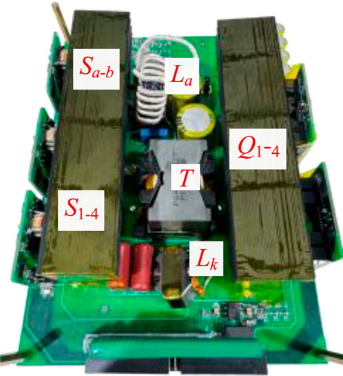
Figure 7. Prototype of the proposed MBDAB converter.
The steady-state experimental waveforms of the MBDAB converter under Vin = 250 V and Vin = 450 V are shown in Figure 8. The voltage across the auxiliary capacitor CBuck, the output voltage of the MBDAB converter, the buck inductor current iLf, and the DAB leakage inductor current are shown in the figure. As can be seen, the output voltage of the MBDAB converter can be stabilized at 48 V. The DAB leakage inductor current iLk indicates that the voltage-matched condition is achieved. The waveforms of the currents are consistent with the theoretical analysis when input voltage varies.
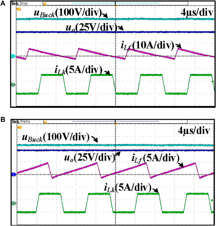
Figure 8. Steady-state waveforms of (A) Vin = 250 V; (B) Vin = 450 V.
The ZVS waveforms of Sa under 250 V input voltage and different loads are shown in Figure 9. The drain–source voltage across Sa, the driving signal of Sa, the buck inductor current, and the DAB leakage inductor current are shown in the figure. As can be seen, drain–source voltage across Sa has dropped to zero before the driving signal arises. As shown in the experimental results, Sa of the buck stage realizes ZVS under 250 V input voltage at both light and heavy loads. The heavy load condition is 1,000 W, and the light load condition is 300 W.

Figure 9. ZVS waveforms of Sa when Vin = 250 V: (A) light load; (B) heavy load.
The ZVS waveforms of Sa under 450 V input voltage and different loads are shown in Figure 10. The drain–source voltage across Sa, the driving signal of Sa, the buck inductor current, and the DAB leakage inductor current are shown in the figure. As can be seen, the drain–source voltage across Sa has dropped to zero before the driving signal arises. As shown in the experimental results, Sa of the buck stage realizes ZVS under 450 V at both light and heavy loads.
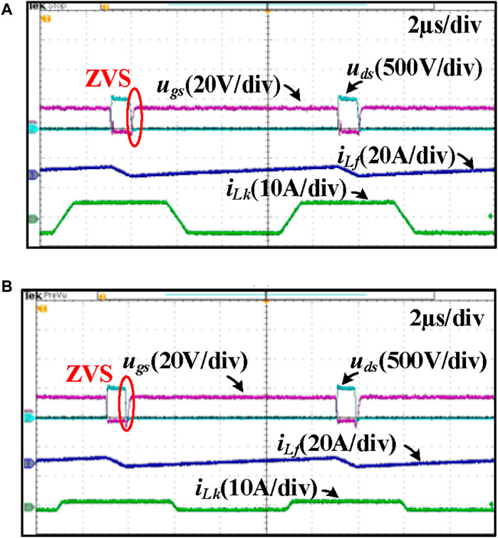
Figure 10. ZVS waveforms of Sa when Vin = 450 V: (A) light load; (B) heavy load.
The ZVS waveforms of S1 under both light and heavy loads are shown in Figure 11. The drain–source voltage across S1, the driving signal of S1, the buck inductor current, and the DAB leakage inductor current are shown in the figure. As can be seen, the drain–source voltage across S1 has dropped to zero before the driving signal arises. As shown in the experimental results, S1 of the DAB stage realizes ZVS under a wide voltage range at both light and heavy loads.
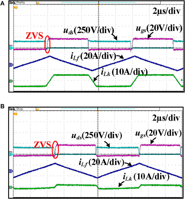
Figure 11. ZVS waveforms of S1 under (A) light load; (B) heavy load.
The ZVS waveforms of S2 under both light and heavy loads are shown in Figure 12. As can be seen, the drain–source voltage across S2 has dropped to zero before the driving signal arises. As shown in the experimental results, S2 of the DAB stage realizes ZVS under a wide voltage range at both light and heavy loads.

Figure 12. ZVS waveforms of S2 under (A) light load; (B) heavy load.
The experimental results of bidirectional power transfer are shown in Figure 13. As can be seen, under forward power transmission mode, the phase of uab is ahead of the phase of ucd, as shown in Figure 13A. In addition, under backward power transmission mode, the phase of uab lags behind the phase of ucd, as shown in Figure 13B.
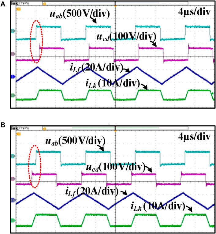
Figure 13. Bidirectional waveforms under 1,000 W: (A) forward mode; (B) backward mode.
The measured efficiency comparisons of the proposed MBDAB converter and the TSBDAB converter are shown in Figure 14. It includes experimental results under different loads and different input voltages. To ensure the fairness of comparison, the input and output voltage and the circuit parameters of the DAB circuit of the TSBDAB converter are the same as the MBDAB converter. In addition, to make a comparison under the same magnetic component, the inductance of the buck inductor in the TSBDAB converter is also designed the same as that in the MBDAB converter. This means that the ZVS condition of the buck part cannot be achieved under some load conditions in the TSBDAB converter. At lower input voltage, the proposed MBDAB converter has a higher efficiency than buck-DAB under a full-load range due to the partial power transmission characteristic. At medium input voltage, the two converters have similar efficiencies due to the similar current of iLf. At higher voltage, the proposed MBDAB converter has a higher efficiency than the buck-DAB converter due to the lower inductor current.
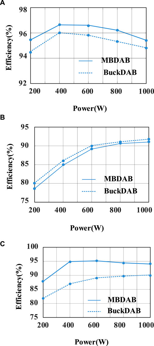
Figure 14. Comparison of measured efficiency of the proposed MBDAB and TSBDAB converters: (A) 250 V; (B) 350 V; and (C) 450 V.
The loss breakdown of the proposed MBDAB converter under different input voltages and different loads is shown in Figure 15. The C3M0045065D of CREE is adopted as the MOSFETs of the primary and secondary switches of the converter. The PQ40-40 and RM10 are used as the inductor and transformer core of DAB. In addition, the inductor type of buck used for the prototype is Kool Mµ Toroid of 77071A7.
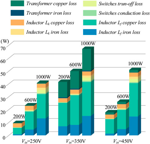
Figure 15. Loss breakdown of the proposed MBDAB converter under different input voltages and different loads.
As shown in the figure, the total loss of the MBDAB converter under 350 V input voltage is higher than that of the input voltages at 250 V and 450 V, which is mainly caused by the increased inductor Lf iron loss. The peak-to-peak and RMS values of the buck inductor current under this operating point are larger. In addition, it can be seen from Figure 13 that the estimated efficiency is basically consistent with the measured efficiency with slightly mismatching. For example, at the output power of 200 W, the estimated losses are 9.4 W, 41.5 W, and 17.8 W at the input voltages of 250 V, 350 V, and 450 V, which are close to the measured efficiencies of 95.3%, 79.2%, and 91.1%, respectively.
5 Conclusion
In this article, a modified two-stage isolated bidirectional buck-DAB converter is proposed. When the input voltage of the MBDAB changes, the front-end buck stage performs gain adjustment, whereas DAB operates under a fixed voltage gain condition. The buck stage can only transmit part of the output power, which is due to the change in the TSBDAB scheme. All the switches of the proposed converter can achieve the ZVS condition. Working principle, voltage gain ratio analysis, power transfer characteristic, and ZVS analysis are introduced for the MBDAB converter.
The experimental results show that the proposed MBDAB converter can realize partial power transmission of the buck stage and ZVS of all switches, which reduces losses of the MBDAB converter effectively.
Data availability statement
The raw data supporting the conclusions of this article will be made available by the authors, without undue reservation.
Author contributions
JL: software and writing–original draft. DW: investigation and writing–review and editing. ZL: methodology and writing–review and editing. GX: validation and writing–review and editing.
Funding
The author(s) declare that financial support was received for the research, authorship, and/or publication of this article. This work was financially supported by the Science and Technology Project of State Grid Hunan Electric Power Company Limited (5216A522000M).
Conflict of interest
Authors JL and DW were employed by State Grid Hunan Electric Power Company Limited Research.
The remaining authors declare that the research was conducted in the absence of any commercial or financial relationships that could be construed as a potential conflict of interest.
The authors declare that this study received funding from State Grid Hunan Electric Power Company Limited. The funder had the following involvement in the study:Thesis preparation, theoretical analysis and design.
Publisher’s note
All claims expressed in this article are solely those of the authors and do not necessarily represent those of their affiliated organizations, or those of the publisher, the editors, and the reviewers. Any product that may be evaluated in this article, or claim that may be made by its manufacturer, is not guaranteed or endorsed by the publisher.
References
Alou, P., Oliver, J., and Cobos, J. A. (2001) “Buck + half bridge (d = 50%) topology applied to very low voltage power converters,” in Annual IEEE Applied Power Electronics Conference and Exposition (APEC).
Doncker, R. W. D., Divan, D. M., and Kheraluwala, M. H. (1988).“A three-phase soft-switched high power density dc/dc converter for high power ap-plications,” in Conference Record of the 1988 IEEE Industry Applications Society Annual Meeting, January-February, 1991 (IEEE), 1, 796–805.
Everts, J. (2017). Closed-form solution for efficient ZVS modulation of DAB converters. IEEE Trans. Power Electron. 32 (10), 7561–7576. doi:10.1109/tpel.2016.2633507
Fu, M., Fei, C., Lee, F. C., and Li, Q. (2020). A GaN-based DC–DC module for railway applications: design consideration and high-frequency digital control. IEEE Trans. Ind. Electron. 67 (2), 1638–1647. doi:10.1109/tie.2019.2896279
Guo, Z. (2020). Modulation scheme of dual active bridge converter for seamless transitions in multi-working modes compromising ZVS and conduction loss. IEEE Trans. Ind. Electron. 67 (9), 7399–7409. doi:10.1109/tie.2019.2945270
Inoue, S., and Akagi, H. (2007). A bidirectional DC–DC converter for an energy storage system with galvanic isolation. IEEE Trans. Power Electron. 22 (6), 2299–2306. doi:10.1109/tpel.2007.909248
Lee, J., Jeong, Y., and Han, B. (2011). An isolated DC/DC converter using high-frequency unregulated $LLC$ resonant converter for fuel cell applications. IEEE Trans. Ind. Electron. 58 (7), 2926–2934. doi:10.1109/tie.2010.2076311
Liao, Y., Xu, G., Peng, T., Sun, Y., Yang, Y., and Xiong, W. (2022). Power-estimation-Based synchronous rectification solution for bidirectional DAB-LLC converter. IEEE Trans. Circuits Syst. II Express Briefs 69 (3), 1213–1217. doi:10.1109/TCSII.2021.3104884
Lin, N., Zhao, Z., Diao, F., Zhao, Y., and Balda, J. C. (2022). A current-fed dual-half-bridge-based composite converter with improved light-load efficiency through a multi-variable optimization. IEEE Trans. Transp. Electrification 8 (2), 3008–3020. doi:10.1109/tte.2021.3126726
Masrur, M. A., Skowronska, A. G., Hancock, J., Kolhoff, S. W., McGrew, D. Z., Vandiver, J. C., et al. (2018). Military-based vehicle-to-grid and vehicle-to-vehicle microgrid—system architecture and implementation. IEEE Trans. Transp. Electrific 4 (1), 157–171. doi:10.1109/tte.2017.2779268
Shao, S., Chen, H., Wu, X., Zhang, J., and Sheng, K. (2019). Circulating current and zvs-on of a dual active bridge dc-dc converter: a review. IEEE Access 7, 50 561–650 572. doi:10.1109/access.2019.2911009
Sun, J., Sun, Q., and Wang, P. (2020). Improved dynamic response strategy with dual phase-shift control for dual-active-bridge DC-DC converter. IET Power Electron. 13 (12), 2671–2674. doi:10.1049/iet-pel.2020.0076
Sun, J., Xu, M., Reusch, D., and Lee, F. C. (2008). “High efficiency quasi-parallel voltage regulators,” in Proc. 23rd annu. IEEE appl. Power electron. Conf. Expo, Austin, TX, USA, February 24–28, 2008 (IEEE), 811–817.
Tu, H., Feng, H., Srdic, S., and Lukic, S. (2019). Extreme fast charging of electric vehicles: a technology overview. IEEE Trans. Transp. Electrific 5 (4), 861–878. doi:10.1109/tte.2019.2958709
Xu, C., Liu, S., and Guo, X. (2020) “A novel converter integrating buck-boost and DAB converter for wide input voltage,” in The 46th Annual Conference of the IEEE Industrial Electronics Society (IECON), Singapore, October 18–21, 2020 (IEEE).
Zhao, B., Song, Q., Liu, W., and Sun, Y. (2014). Overview of dual-active-bridge isolated bidirectional DC–DC converter for high-frequency-link pow-er-conversion system. IEEE Trans. Power Electron. 29 (8), 4091–4106. doi:10.1109/tpel.2013.2289913
Zhao, B., Yu, Q., and Sun, W. (2012). Extended-phase-shift control of isolated bidirectional DC-DC converter for power distribution in microgrid. IEEE Trans. Power Electron. 27 (11), 4667–4680. doi:10.1109/tpel.2011.2180928
Keywords: isolated DC/DC converter, modified two-stage, buck-DAB converter, zero-voltage switching, bidirectional converter
Citation: Li J, Wan D, Lu Z and Xu G (2024) A modified two-stage isolated bidirectional buck-DAB converter with a full-load ZVS range. Front. Energy Res. 12:1429713. doi: 10.3389/fenrg.2024.1429713
Received: 08 May 2024; Accepted: 17 June 2024;
Published: 15 July 2024.
Edited by:
Yushuai Li, Aalborg University, DenmarkReviewed by:
Xiang Li, Zhengzhou University, ChinaZheng Lan, Hunan University of Technology, China
Zhongting Tang, Aalborg University, Denmark
Copyright © 2024 Li, Wan, Lu and Xu. This is an open-access article distributed under the terms of the Creative Commons Attribution License (CC BY). The use, distribution or reproduction in other forums is permitted, provided the original author(s) and the copyright owner(s) are credited and that the original publication in this journal is cited, in accordance with accepted academic practice. No use, distribution or reproduction is permitted which does not comply with these terms.
*Correspondence: Zhengmei Lu, bHV6aGVuZ21laUBjc3UuZWR1LmNu