 Zhiyong Chen1
 Qunying Liu
- 1Economic and Technical Research Institute of State Grid Hebei Electric Power Co., Ltd., Shijiazhuang, China
- 2School of Automation Engineering, University of Electronic Science and Technology of China, Chengdu, China
The high inductance current ripple and the PV voltage fluctuations limitation at the DC (direct current) -DC link have been the unsolved problems in the photovoltaic systems tied in grid. A control strategy with a current hysteresis loop is proposed to address the issues of high inductance current ripple in photovoltaic systems which can achieve real-time duty cycle regulation. Differing from the conventional mode that uses one switch in the buck–boost DC–DC link, two switches have been designed here to separate the buck and boost modes for the coordinated control, which can achieve a wide PV voltage fluctuations range. Based on the conventional fixed-duty cycle determination method, a real-time duty cycle determination method is proposed by introducing changes in inductance current. In order to improve power conversion efficiency, the incremental conductance method is improved by introducing the steepest gradient descent to quickly achieve the maximum power point tracking. This study experimentally verifies the proposed current hysteresis coordinated control method, effectively suppressing the ripple of the inductor current and expand the PV voltage fluctuation in the DC–DC link on the basis of maintaining power conversion efficiency as much as possible.
1 Introduction
In the last 20 years, many studies have focused on the topology of DC–DC links and converter technology for the DC–AC interface of photovoltaic (PV) cells and the grid. DC–AC interface technology has included voltage source converters (VSIs) adapted for the interface of PV panels with the grid (Teodorescu et al., 2011). To address the constraint of low leakage current for non-isolated grid-tied converters, a series of different converter structures and control schemes have been investigated (Alluhaybi et al., 2020; Khan et al., 2020), some considering stochasticity (Nan et al., 2018). In addition to converter configuration reformation, the topology and control strategy of the DC–DC link is also a key area of improvement for less harmonics and higher transferring efficiency. Liao et al. (2017) proposed a novel PV converter with a PV current decoupling strategy which can achieve maximum power point tracking performance without increasing electrolyte capacitance. The current decoupling tank in the proposed PV converter can buffer the difference between the DC current generated by the PV panel and the rectified sinusoidal AC of the power grid. Mohammadi et al. (2018) proposed a novel switching frequency modulation method to address the trade-off between voltage gain and voltage harmonics caused by the coupling of the duty cycle and modulation ratio. Ho and Siu (2019) proposed a new converter structure in which high-frequency switches are used to control the inductor current, while low-frequency switches form a filter structure that adapts to different operating conditions. Unfortunately, the designed structure led to more energy loss.
The output voltage of PV panels is often affected by ambient factors such as sunlight intensity, temperature, and shadow. A buck–boost converter is required to adapt to a wide range of DC voltage fluctuations. Callegaro et al. (2019) proposed a single-phase, single-stage buck–boost converter which uses five switches (implemented using MOSFET power with external fast recovery diodes) to provide buck–boost operation for the wide range of changes in PV output voltage while eliminating leakage current. In order to improve power extraction under the ambient condition, a buck–boost single-phase transformer-free grid-connected photovoltaic converter based on coupled inductance has been proposed by Kumar and Singh (2019) and Hafiz et al. (2021) which has the ability to extract maximum power from the series of photovoltaic panels. Dutta and Chatterjee (2018) proposed a day-and-night operational single-phase energy stored quasi-Z-source-cascaded H-bridge (ES-qZS-CHB) converter PV system to solve the active and reactive power control problem. They designed optimal multiple combinations of duty cycle and modulation ratio to achieve the same voltage gain during night operation.
In order to balance the output voltage of input-independent-output series modules, bidirectional buck–boost and LC series power balancing units have been proposed for multiple PV panels by Dutta and Chatterjee (2020). Liang et al. (2021) proposed a multi-PV panel with battery and bidirectional converter interconnected with a three-phase grid. A buck–boost converter is connected to the main VSC with BES is responsible for the load level adjusting and the MPPT voltage. A new solar PV-fed dynamic voltage restorer (DVR) based on a trans-Z-source converter was proposed by Huang et al. (2021) to improve the power quality of on-grid PV systems, in which a hybrid unit vector template with maximum constant boost control method was proposed for transZSI-DVR. Chauhan et al. (2021) outlined an integrated three-phase transformer-less PV converter structure which utilizes an interleaved dual output buck–boost converter to obtain the boosting voltage. From a single PV source, the voltage waveform of the output terminal can be synthesized into three levels; the high-frequency dynamic is completely eliminated when the voltage passes through parasitic capacitors, effectively suppressing current leakage.
On the basis of a buck–boost circuit, coupling inductance has been proposed by Ali et al. (2021) to regulate power output, forming a secondary voltage gain adjustment strategy. In order to reduce the leakage current and number of components and to improve transfer efficiency, a transformer-free converter structure based on MOSFET power switches was proposed by Dhara and Somasekhar (2022); it shares a common ground between the PV source and grid and applies a zero-beat controller instead of a PI controller. In Yari et al. (2022), a three-phase multi-level converter based on three-level neutral point clamp quasi Z-source topology was proposed to implement maximum power tracking. These methods give almost no or very little consideration for energy conversion efficiency.
In order to achieve high efficiency and negligible loss during high-frequency switching, Gao et al. (2022) proposed a buck–boost PV converter structure with six switches which operates at different frequencies under a discontinuous mode with zero current leakage. A new seven-level common ground (CG) switched capacitor (SC)-based grid-tied transformer-less converter was introduced in Husev et al. (2022) which has three times the boosting capability of input voltage. To step up the input PV voltage and facilitate seven steps in output voltage, two SC cells are connected in parallel.
Inspired by the research outlined above, we designed a buck–boost structure and propose an effective coordinated control in DC–DC and DC–AC to improve power conversion efficiency and reduce harmonics. The configuration and operation mechanism of the PV converter with buck–boost DC links is analyzed in the second section. The third section discusses a coordinated control strategy with the current hysteresis loop on the DC–DC link and converter. To validate the superiority of the proposed coordinated control strategy with the current hysteresis loop strategy, a rigorous experimental evaluation was conducted by designing a rapid control prototype (RCP) framework which gives the simulation verification of the designed converter and the proposed coordinated control strategy, detailed in the fourth section. Conclusions are drawn in the fifth section.
2 Analysis of the structure and operating mechanism of photovoltaic converters based on a buck–boost DC link
The circuit structure of a buck–boost converter with a single photovoltaic (PV) panel is shown in Figure 1. The coordinated current hysteresis control proposed in this paper mainly controls the S1 and S2 switches of the DC link to accelerate its dynamic response ability; these are independently controlled with the converter switches S3–S8. The rationality of the switch control design in the DC–DC link directly affects the quality of the voltage output by the converter. Therefore, the focus here is on the switch control of the DC–DC link while ensuring that the converter switch is normally turned on or off.
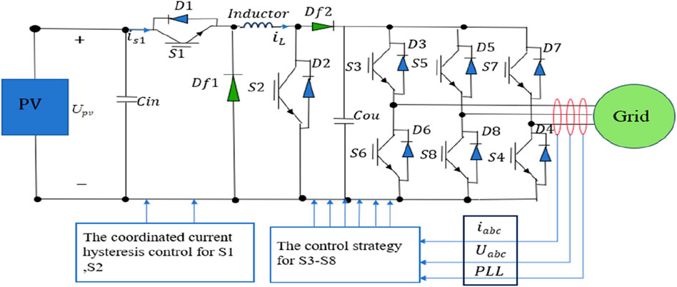
Figure 1. Circuit structure of the buck–boost converter with a single photovoltaic panel.
The current hysteresis control belongs to PWM (pulse width modulation) tracking technology, the basic idea of which is to compare the controlled variable (usually including the output voltage or the inductor current in the DC–DC link) with its given value. If the difference between the controlled variable and its given value is greater than the set upper limit value, the switch state is changed to reduce the controlled variable. If their difference is less than a set lower limit value, the switch state is changed to increase the controlled quantity. If their difference is between the lower and upper limits, the switch will be kept on. Therefore, the current hysteresis control belongs to the closed-loop control, which has the characteristics of real-time control and fast response speed. Moreover, by changing the upper and lower limits of error, tracking accuracy can be easily controlled. In fact, the current hysteresis control is a non-linear control that can significantly improve the non-linear dynamic performance of the converter. Considering that the PV systems are easily affected by environmental factors such as sunlight, temperature, and cloud cover, the variation range of the output voltage at the PV panel is relatively wide, which can lead to large fluctuations in inductance current. Therefore, the buck–boost converter using inductance current hysteresis control is introduced to adjust the PWM output signal based on the grid current as a reference in hysteresis control, thereby adjusting the duty cycle of the high-frequency switch and adjusting the inductance current in the buck–boost DC link.
In our work, the current hysteresis control of the DC–DC link introduces a current deviation detection loop comprising a limiting loop and a hysteresis comparison loop. Introducing the two loops creates a relationship between output voltage, output current, and inductor current, forming the current hysteresis control strategy based on the changes in output voltage, current, and inductor current to coordinate the on/off modes of S1 and S2 and limit the amplitude of the inductor ripple current. By using the current hysteresis control, sudden changes in input voltage will not have any impact on the average output voltage, only on ripple. Here, current hysteresis control is introduced. The control flow chart of the current hysteresis control is shown as Figure 2. When the transient current of the inductor exceeds a certain range
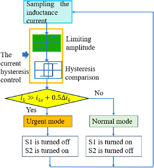
Figure 2. Control flow chart of the current hysteresis control.
Figure 3 shows the discrimination in the buck–boost mode. To select this mode, the corresponding switching signal needs to be given. Determining the buck or boost mode completely depends on the comparison of the voltage of capacitor
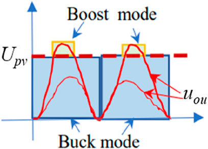
Figure 3. Buck and boost mode discrimination.
According to the operating characteristics of the buck–boost converter under different operating modes, its operating mechanism is elaborated in detail as follows.
2.1 Buck mode:
In Figure 4A, the voltage at the PV panel port is equivalent to the DC source
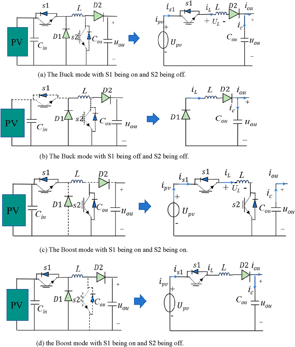
Figure 4. Equivalent circuit for buck and boost mode. (A) Buck mode with S1 on and S2 off. (B) Buck mode with S1 and S2 off. (C) Boost mode with S1 and S2 on. (D) Boost mode with S1 on and S2 off.
According to Equation 2 the relationship between inductance current and voltage can be represented as Equation 3.
According to Equation 3, further deformation can be carried out to obtain Equation 4.
where
where d1 is the ideal duty cycle of S1. The triggering pulse of S1 synchronizes with the phase change of the
where
Let setting
The average current passing through S1 in one switching cycle is Equation 9.
When the driving signal of switch S1 is turned to a low level, the switch is turned off, and the inductor L is discharged through the freewheeling diode D1. The inductor current gradually decreases, and the inductor voltage reverses to resist the decrease in inductor current. The output voltage is maintained by the discharge of the capacitor
When S1 is turned off, the inductor is discharged until S1 and S2 turn on again.
2.2 Boost mode:
According to the equivalent circuit of the boost mode with S1 and S2 both on (Figure 4C) with
According to Equation 12, the change of the inductor current is calculated as Equation 13.
where
When S1 turns on and S2 turns off, the equivalent circuit is shown in Figure 4D, which is the same as Figure 4A. The inductor is continuously charged, and the capacitor also starts to be charged after discharging for
Because
Then, the capacitor voltage amplitude of the DC–DC link can be calculated as Equation 17.
The voltage amplitude of the capacitor is calculated to perform the operation mode discrimination for buck or boost mode in the coordinated control algorithm with the current hysteresis loop.
3 DC–DC coordinated control strategy with the current hysteresis loop
When the insolation changes,
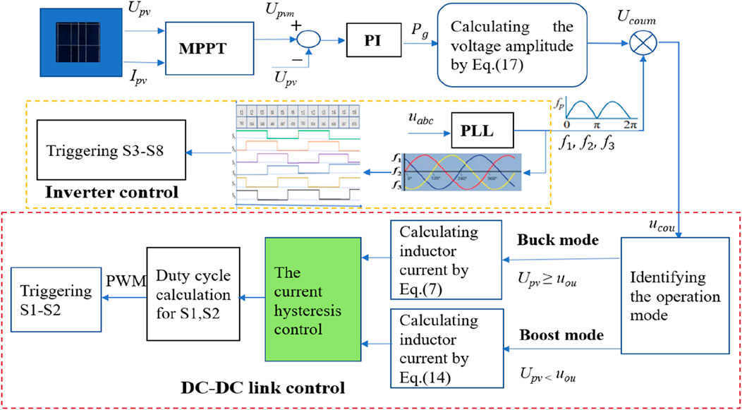
Figure 5. Block diagram of the coordinated control method for the whole PV converter.
The whole control diagram includes the converter control and DC–DC link control. In the converter control, the phase-locked loop (PLL) samples the three-phase voltage at the grid side to obtain the three-phase voltage waveform of the grid as f1, f2, and f3, based on the triggering pulse sequences and duty cycles of the S3–S8 switches of the converter. In the DC–DC link control, the MPPT module collects the
To maintain a constant output voltage, the converter control needs to track the voltage changes in the grid-tied point and adjust the switch sequence of S3–S8. To obtain the three-phase sinusoidal voltage at the terminal of the converter, the S3–S8 switches of the converter must follow a certain triggering sequence and duration to maintain synchronization with the voltage of the grid-tied point. Figure 6 shows the designed triggering sequence for S3–S8.
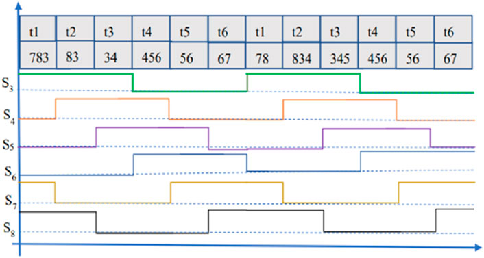
Figure 6. Trigger timing sequence and duty cycle length of S3–S8.
The maximal power point tracking algorithm in the MPPT module for the PV system includes the incremental conductance method (INC) and the perturb and observe algorithm (P&O). P&O belongs to the local search algorithms and is susceptible to noise and shadow interference. Compared with P&O, INC shows a fast response but is prone to impact by the step size and sampling frequency.
Therefore, the steepest gradient factor is combined to improve the search speed of the maximal power point. As shown in Figure 7, the first step is to determine the gradient factor, so the steepest gradient factor expression is set as Equation 18.
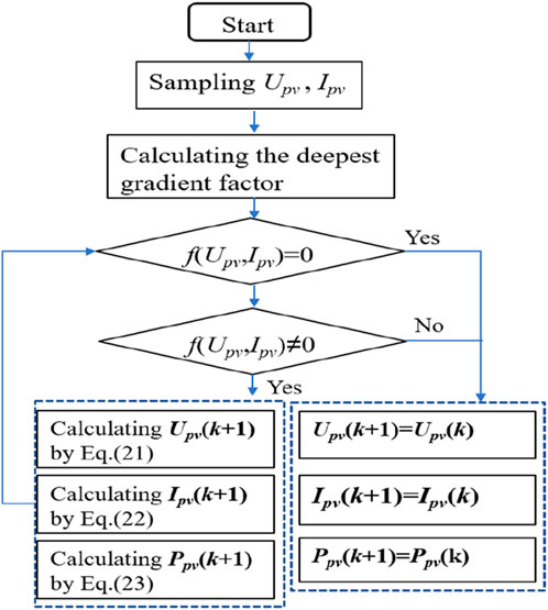
Figure 7. Maximum power point search algorithm based on steepest gradient descent.
where k+1, k, and k-1 are the sampling time.
4 Simulation and experimental verification
To verify the practicability of grid-tied PV system operation for the proposed buck–boost structure and the coordinated control strategy with the current hysteresis loop, the component parameters are set as per Table 1. The HNZL DC power supply has been used to imitate the effect of insolation. In order to emulate simultaneous variation in temperature and in the level of insolation, the MPP parameters are set as follows:
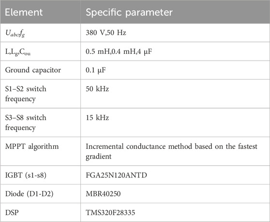
Table 1. Parameter of photovoltaic converter with buck–boost.
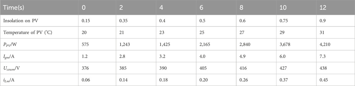
Table 2. Changes in voltage, current, and power parameters of photovoltaic panels under different insolations.
Figure 8 shows the relationship of the active power output and the voltage changes by the PV curves under different temperatures. When the temperature is lower, the power emitted is greater for the PV panel with the PV panel voltage being improved. When the voltage reaches 438 V, the active power output of the PV panel reaches the maximum point at 30 °C, which is consistent with the estimated value. During the MPPT process of this experiment, the maximum power point search algorithm based on steepest gradient descent takes only 0.22s to reach the maximum power point C, which is shorter than the common incremental conductance method, which is 0.31s to reach point C. This is because the improved maximum power point search algorithm based on the steepest gradient descent only searches the process from points A to C, avoiding the searching process from C to B and B to C, which saves search time. However, the common incremental conductance method tends to search from A to C, C to B, and B to C.
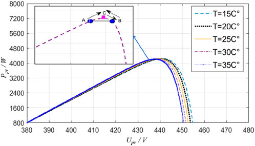
Figure 8. Simulated PV curves under different temperatures.
Figures 9A–C show the simulated changes in
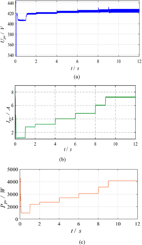
Figure 9. Simulated PV panel port states under different insolations: (A) voltage
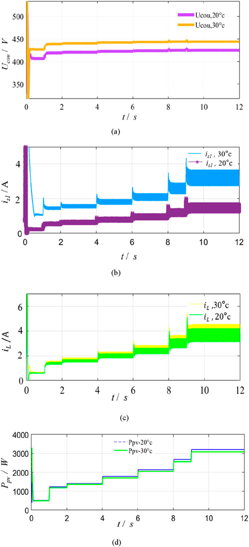
Figure 10. Simulated DC–DC link state curves under different temperatures: (A) voltage
Figure 11 shows the simulated voltage and current curve at the PV grid-collection points at 30 °C with changed insolation. This shows that the insolation will impact the output power of the converter. When the insolation becomes strong, the output current of the converter increases, while the voltage of the converter remains stable; hence, the output power of the converter increases at the same time. Figure 12 compares the inductor current change when the current hysteresis control is introduced in the coordinated control under the same insolation. During the dynamic process, the ripple current of the inductor is controlled at a relatively satisfactory level, demonstrating the effectiveness of the introduced current hysteresis control. The power conversion efficiency of the PV panel is the percentage of the injected power at the grid-connection point to the output power of the PV panel. The referred voltage and current from the PV panel and grid-tied point are all at the averaging value. Figure 13 is the prototype of the designed buck–boost converter. Under the condition of the converter being off-grid, the experimental waveforms for Ug and ig are shown in Figure 14, in which, when the input voltage of DC–DC changes from 50 V to 100 V,
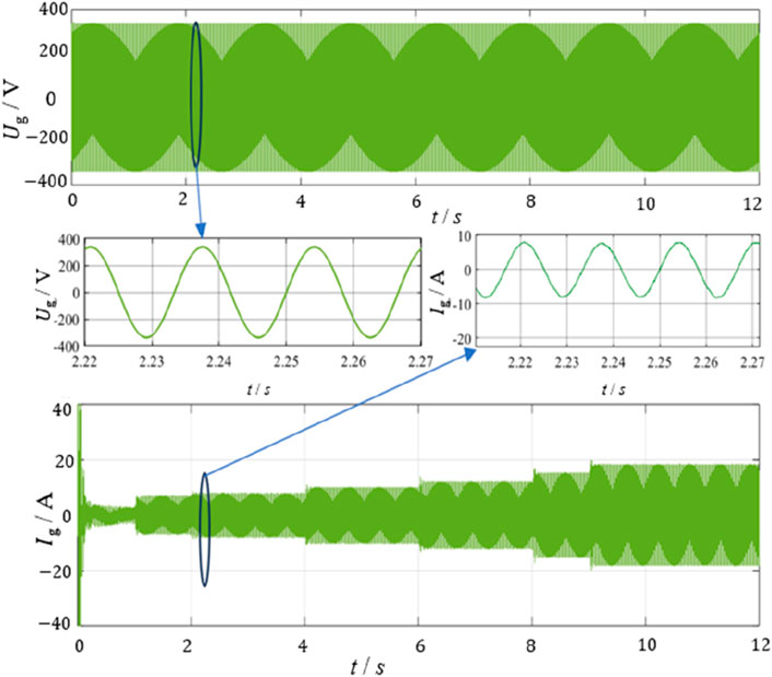
Figure 11. Simulated voltage and current curve at photovoltaic grid-collection points at 30 °C with changed insolation.
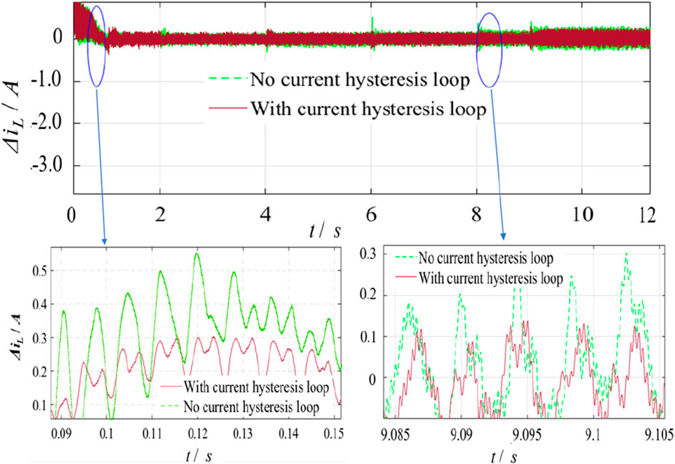
Figure 12. Simulated inductor current suppression comparison under same insolation.
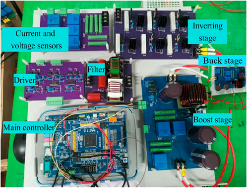
Figure 13. Prototype of the designed buck–boost converter.
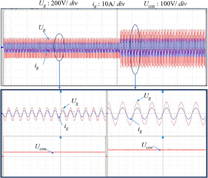
Figure 14. Experimental waveforms for Ug, ig, and
Figure 15 shows the comparison results between the actual and estimated conversion efficiency of the PV converters, from which it can be inferred that the estimated value tends to consider the ideal situation and ignore the actual ambient condition, resulting in overestimated efficiency. At the maximal power point of 700 W, the actual conversion efficiency is just 97.8%, lower than the estimated value of 98.7%. To further assess the impact of the current hysteresis loop on conversion efficiency, those efficiencies with current hysteresis and without hysteresis are calculated. Figure 16 shows that during the period of low power output, the conversion efficiency with the current hysteresis loop is almost the same as that without current hysteresis loop control. However, with the active power output of the PV panel increasing, the conversion efficiency considering the current hysteresis loop decreases. This means that the increasing active power output corresponds to the increasing inductor current, which is suppressed by the current hysteresis loop at the cost of conversion efficiency. Figure 17 shows the THD comparison curves between the method in Dutta and Chatterjee (2018) and the proposed method here. According to the datum, the changing trend of the THD in the grid-tied point with the output voltage increase of the PV panel remains consistent in the two methods. However, the THD in the proposed method is lower than in Dutta and Chatterjee (2018). Furthermore, the voltage variation range dealt by the method proposed here is 120 V–600 V, with a wider variation range than that in Dutta and Chatterjee (2018). The active power losses at different power levels are also calculated (Figure 18). The comparison results imply that the active power loss values in our method and in Dutta and Chatterjee (2018) are almost the same when the output power of the PV panel is below 1,700 W. Then, with the output power of the PV panel increasing, the active power loss in Dutta and Chatterjee (2018) is higher than the method proposed here, especially when the output power is more than 3,200 W. This shows that the designed converter can adopt higher power production. The above results verify that the designed buck–boost PV converter with the coordinated control strategy has improved operational performance.
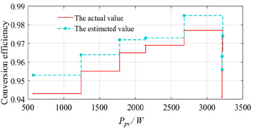
Figure 15. Comparison curve between the actual conversion efficiency and estimated conversion efficiency of photovoltaic converters.
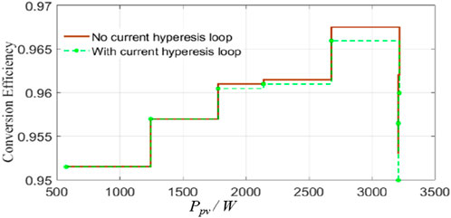
Figure 16. Comparison of the conversion efficiency between photovoltaic panels with or without current hysteresis.
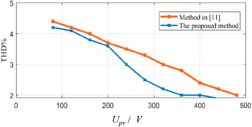
Figure 17. Comparison of the THD ratio of the method in Dutta and Chatterjee (2018) and the method proposed here.
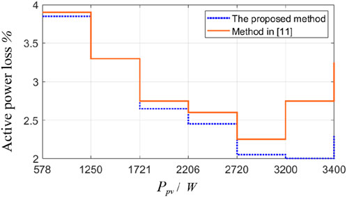
Figure 18. Loss distribution at different power levels.
5 Conclusion
A buck–boost converter structure and corresponding coordinated control strategy is designed for a grid-tied photovoltaic (PV) panel in this paper. By simulation and experimental verification, the following conclusions are drawn.
(1) To improve the robustness and easing the requirement for PWM dead-times, a wide range buck–boost operation for large fluctuations in PV voltage is provided, and large buck–boost inversions are obtained with relatively smaller duty ratios. Through the operational performance comparison with the classical buck–boost converter, the buck and boost stages in the DC–DC link are decoupled and controlled separately through two switches, which is beneficial for expanding the voltage conversion range of the DC–DC link. However, the designed converter can withstand overlap time in complementary switches without voltage shoot-through problems. At the same time, the incremental conductance method is improved by introducing the deepest gradient factor, which improves the search speed of the maximum power point and enhances the dynamic performance of the converter.
(2) Considering the significant fluctuation of inductor current in the boost stage, a DC–DC coordinated control scheme based on current hysteresis control is here proposed. Based on traditional duty cycle calculation, the influence of the inductor current is introduced, and a duty cycle adjustment based on the current hysteresis control is performed to reduce the ripple of the inductor current at the cost of reducing the conversion efficiency of the PV converter. However, by comparison with the classical buck–boost converter, the designed converter shows noticeable improvement in the THD ratio with the input voltage increase of the DC–DC link. Furthermore, the active power loss caused by the designed converter is also reduced by the coordinated control strategy.
However, under conditions of partial shading, the efficiency of the designed converter is still greatly decreased, the reduction depending on the size of the shading area. The PV ground leakage current is still another unsolved problem in our scheme. Further research should focus on diminishing the leakage current, improving the power conversion efficiency of multiple PV panel series, and suppressing common mode currents under voltage imbalance caused by different insolation conditions and shadowing.
Data availability statement
The original contributions presented in the study are included in the article/supplementary material; further inquiries can be directed to the corresponding author.
Author contributions
ZC: writing–review and editing, conceptualization, investigation, and methodology. ZH: conceptualization, project administration, resources, and writing–original draft. JA: conceptualization, methodology, visualization, and writing–review and editing. WF: visualization, data curation, investigation, and writing–original draft. YH: visualization, writing–review and editing, and methodology. QL: writing–review and editing, writing–original draft, and conceptualization.
Funding
The authors declare that financial support was received for the research, authorship, and/or publication of this article. This paper is supported by the project of Economic Research Institute of State Grid Hebei Electric Power Co., Ltd., grant number is SGHEJY00GHJS2310078.
Conflict of interest
Authors ZC, ZH, JA, WF and YH were employed by State Grid Hebei Electric Power Co., Ltd.
The remaining author declares that the research was conducted in the absence of any commercial or financial relationships that could be construed as a potential conflict of interest.
The authors declare that this study received funding from Economic and Technical Research Institute of State Grid Hebei Electric Power Co., Ltd. The funder had the following involvement in the study: collection, analysis, interpretation of data.
Publisher’s note
All claims expressed in this article are solely those of the authors and do not necessarily represent those of their affiliated organizations, or those of the publisher, the editors, and the reviewers. Any product that may be evaluated in this article, or claim that may be made by its manufacturer, is not guaranteed or endorsed by the publisher.
References
Ali, M., Padmanaban, S., Ramachandaramurthy, V. K., MitoloO, M., and Benbouzida, M. (2021). A novel solar photovoltaic fed TransZSI-DVR for power quality improvement of grid-connected PV systems. IEEE Access:Special Sect. Evol. Technol. Energy Storage Syst. Energy Syst. Appl. 9, 7263–7279. doi:10.1109/access.2020.3048022
Alluhaybi, K., Batarseh, I., Hu, H., and Chen, X. (2020). Comprehensive review and comparison of single-phase grid-tied photovoltaic microinverters. IEEE J. Emerg. Sel. Top. Power Electron. 8 (2), 1310–1329. doi:10.1109/jestpe.2019.2900413
Arup, R. P., Bhattacharya, A., and Chatterjee, K. (2023). A single-phase grid-connected boost/buck–boost-derived solar PV micro-inverter topology having power decoupling capability. IEEE J. Emerg. Sel. Top. Power Electron. 11 (2), 2340–2349. doi:10.1109/jestpe.2023.3234070
Callegaro, L., Ciobotaru, M., Pagano, D. J., and Fletcher, J. E. (2019). Feedback linearization control in photovoltaic module integrated converters. IEEE Trans. Power Electron. 34 (7), 6876–6889. doi:10.1109/tpel.2018.2872677
Chauhan, S., Singh, B., and Singh, B. (2021). Control of three-phase grid integrated multiple solar photovoltaic arrays-BES based MG. IEEE Trans. Industry Appl. 57 (6), 6167–6181. doi:10.1109/tia.2021.3109843
Dhara, S., and Somasekhar, V. T. (2022). A three-phase semi-single stage PV inverter with voltage boosting and leakage current minimization. IEEE Trans. Circuits Systems—II Express Briefs 69 (1), 169–173. doi:10.1109/tcsii.2021.3082580
Dutta, S., and Chatterjee, K. (2018). A Buck and boost based grid connected PV inverter maximizing power yield from two PV arrays in mismatched environmental conditions. IEEE Trans. Industrial Electron. 65 (7), 5561–5571. doi:10.1109/tie.2017.2774768
Dutta, S., and Chatterjee, K. (2020). A coupled inductor-based buck–boost type grid connected transformerless PV inverter having the ability to control two subarrays simultaneously. IEEE Trans. Industrial Electron. 67 (7), 5543–5553. doi:10.1109/tie.2019.2931512
Gao, N., Jin, Z., Wang, H., Wu, W., Koutroulis, E., Chung, H.S.-H., et al. (2022). MOSFET-Switch-Based transformerless single-phase grid-tied inverter for PV systems. IEEE J. Emerg. Sel. Top. Power Electron. 10 (4), 3830–3839. doi:10.1109/jestpe.2021.3064587
Hafiz, F. A., El Moursi, M. S., Zahawi, B., and Hosani, K.A. (2021). Single-phase photovoltaic inverters with common-ground and wide buck–boost voltage operation. IEEE Trans. Industrial Inf. 17 (12), 8275–8287. doi:10.1109/tii.2021.3066511
Ho, C., and Siu, K. (2019). Manitoba inverter—single-phase single-stage buck-boost VSI topology. IEEE Trans. Power Electron. 34 (4), 3445–3456. doi:10.1109/tpel.2018.2855560
Huang, Y., Liu, F., Zhuang, Y., Diao, X., Liu, Z., Pan, S., et al. (2021). Bidirectional buck-boost and series LC-based power balancing units for photovoltaic DC collection system. IEEE J. Emerg. Sel. Top. Power Electron. 9 (6), 6726–6738. doi:10.1109/jestpe.2021.3074575
Husev, O., Vinnikov, D., Roncero-Clemente, C., Blaabjerg, F., and Strzelecki, R. (2022). MPPT and GMPPT implementation for buck-boost mode control of quasi-Z-source inverter. IEEE Trans. Power Electron. 69 (11), 11348–11358. doi:10.1109/tie.2021.3125658
Khan, M. N. H., Forouzesh, M., Siwakoti, Y. P., Li, L., Kerekes, T., and Blaabjerg, F. (2020). Transformerless inverter topologies for single-phase photovoltaic systems: a comparative review. IEEE J. Emerg. Sel. Top. Power Electron. 8 (1), 805–835. doi:10.1109/jestpe.2019.2908672
Kumar, S., and Singh, B. (2019). Self-normalized-estimator-based control for power management in residential grid synchronized PV-BES microgrid. IEEE Trans. Industrial Inf. 15 (8), 4764–4774. doi:10.1109/tii.2019.2907750
Liang, W., Liu, Y., and Peng, J. (2021). A day and night operational quasi-Z source multilevel grid-tied PV power system to achieve active and reactive power control. IEEE Trans. Power Electron. 36 (1), 474–492. doi:10.1109/tpel.2020.3000818
Liao, C.-Y., Lin, W.-S., Chen, Y.-M., and Chou, C.-Y. (2017). A PV micro-inverter with PV current decoupling strategy. IEEE Trans. Power Electron. 32 (8), 6544–6557. doi:10.1109/tpel.2016.2616371
Mohammadi, M., Moghani, J. S., and Milimonfared, J. (2018). A novel dual switching frequency modulation for Z-source and quasi-Z-source inverters. IEEE Trans. Industrial Electron. 65 (6), 5167–5176. doi:10.1109/tie.2017.2784346
Nan, Y., Di, Y., Zhou, Z., Jiazhan, C., Daojun, C., and Xiaoming, W. (2018). Research on modelling and solution of stochastic SCUC under AC power flow constraints. IET Generation Transm. and Distribution 12 (15), 3618–3625. doi:10.1049/iet-gtd.2017.1845
Srivastava, A., and Seshadrinath, J. (2023). A single-phase seven-level triple boost inverter for grid-connected transformerless PV applications. IEEE Trans. Industrial Electron. 70 (9), 9004–9015. doi:10.1109/tie.2022.3215815
Teodorescu, R., Liserre, M., and Rodríguez, P. (2011). Grid converters for photovoltaic and wind power systems. New York, NY, USA: Wiley.
Keywords: photovoltaic panel, coordinated control strategy, current hysteresis loop control, buck-boost circuit, DC-DC link
Citation: Chen Z, Hao Z, An J, Fan W, Huang Y and Liu Q (2024) Research on a coordinated control strategy of three-phase photovoltaic converters based on a buck–boost DC link. Front. Energy Res. 12:1428524. doi: 10.3389/fenrg.2024.1428524
Received: 06 May 2024; Accepted: 11 September 2024;
Published: 04 October 2024.
Edited by:
Chenghong Gu, University of Bath, United KingdomReviewed by:
Runze Wu, North China Electric Power University, ChinaFan Chen, Nanjing Institute of Technology (NJIT), China
Roberto Francisco Coelho, Federal University of Santa Catarina, Brazil
Copyright © 2024 Chen, Hao, An, Fan, Huang and Liu. This is an open-access article distributed under the terms of the Creative Commons Attribution License (CC BY). The use, distribution or reproduction in other forums is permitted, provided the original author(s) and the copyright owner(s) are credited and that the original publication in this journal is cited, in accordance with accepted academic practice. No use, distribution or reproduction is permitted which does not comply with these terms.
*Correspondence: Qunying Liu, bHF5MTIwNkAxMjYuY29t