 Awadesh Kumar Mallik1,2,3*
 Kamatchi Jothiramalingam Sankaran1,2,4
 Derese Desta1,2Paulius Pobedinskas1,2Rani Mary Joy1,2Rozita Rouzbahani1,2Fernando Lloret1,2,5Hans-Gerd Boyen1,2Ken Haenen1,2
- 1Institute for Materials Research (IMO), Hasselt University, Diepenbeek, Belgium
- 2IMOMEC, IMEC vzw, Diepenbeek, Belgium
- 3Currently at Nanyang Technological University, Singapore, Singapore
- 4Currently at Institute of Minerals and Materials Technology, Bhubaneswar, India
- 5Currently at Dpt. Física Aplicada, Universidad de Cádiz, Puerto Real, Spain
Integrating chemical vapour deposition (CVD) diamond with GaN material for effective thermal management of the power electronic devices is critical. However, there are issues with CVD processing, like GaN substrate etching under normal CVD diamond growth conditions, which nowadays, is overcome by inserting an intermediate silicon nitride layer of very low thermal conductivity. Unfortunately, such a buffer layer is detrimental to proper heat dissipation. So, the direct growth of diamonds onto GaN substrates is still a relevant research topic. Here, we have used an innovative low-temperature growth process by linear antenna microwave plasma enhanced CVD to overcome such a problem. Other than the normal hydrogen gas CVD recipe, PH3 gas diluted with hydrogen (1,000 ppm in H2) was added as a doping gas precursor, to dope the diamond lattice with phosphorous atoms, by varying the substrate temperature from 400oC to 900oC. PH3 addition in the precursor gas recipe was found to etch the GaN substrate substantially. The phosphorous atom was found to be present on the surface of the diamond film from their corresponding X-ray photoelectron spectroscopy signal. Raman spectroscopy and scanning electron microscopy images do not reveal GaN substrate damage when pure hydrogen gas was used as a precursor without PH3 addition. However, there is a relative competition between the GaN substrate decomposition and CVD diamond growth rates when diluted PH3 gas was used in the precursor gas recipe. At a lower substrate temperature of 400oC, GaN etching was prevalent, but with a gradual increase in substrate temperature to 900ºC, diamond lateral growth was promoted inside the linear antenna CVD reactor, which partially protected the underneath GaN/sapphire heterostructures from decomposition under harsh plasma CVD conditions.
1 Introduction
1.1 GaN substrates
There are non-diamond substrates (Degutis et al., 2015) incompatible with diamond growth due to the harsh CVD processing conditions. The temperature window of 700o-1200°C, which is suitable for the metastable growth of the CVD diamond phase, is detrimental for many low melting point substrates, for example, polymers. Many inorganic substrates are also reactive at such high temperatures of CVD diamond processing. GaN (Oba and Sugino, 2001; Mohapatra et al., 2008) is a reactive substrate prone to etching beyond 600°C (Zhang et al., 2018). It has been proposed by May et al. (2006) that the following three possible reactions occur under a CVD growth environment:
1.
2.
3.
Therefore, it is essential that the CVD growth temperature does not reach temperatures beyond 800°C to avoid any unwarranted damage to the GaN substrate. There is a competition between the rate of diamond deposition and GaN substrate etching. To prevent damage to the substrate, the obvious approach is to put an intermediate buffer layer. Many groups have tried different combinations of nitrides. The most effective so far has been SiN interlayer (Yates et al., 2018; Zhou et al., 2017a; Seelmann-Eggebert et al., 2001; Bland et al., 2019). Based on diffusion mismatch theory and molecular dynamic simulations, due to the phonon density of states mismatch between diamond and GaN, an interlayer is crucial to match the phonon modes on both sides. (Woo et al., 2023; Field et al., 2020; Mu et al., 2022; Sun et al., 2015; Wang et al., 2013). The heat generated due to current flow through GaN devices must be dissipated away to perform efficiently for long periods (Zhou et al., 2017b; Ejeckam et al., 2014; Pobedinskas et al., 2022).
Diamond, being the best heat conductor, is the obvious choice of material to extract away the heat from GaN (Francis et al., 2022; Sang, 2021; Mendes et al., 2022; Gu et al., 2021). The primary obstacle to integrating two dissimilar materials is their difference in crystal lattices and unmatching coefficient of thermal expansion–which are thereby overcome by putting an intermediate transition layer (Francis et al., 2010). The intermediate layer acts as a thermal resistance to heat flow at the respective interfacial boundaries. Sun et al. showed a variation in thermal boundary resistance (TBR) with SiN thickness (Sun et al., 2015). Zhou et al. optimized such a barrier layer and showed that the lowest TBR was obtained with ultra-thin 5 nm SiN (Zhou et al., 2017a). There are experimental reports that confirmed the TBR between diamond and GaN can be lower than 3 m2K/GW by using 1 nm SiN in between. This value is very close to the theoretical value of TBR between diamond and GaN (Malakoutian et al., 2021). SiN having low thermal conductivity (1.18 W/m.K) would still act as thermal insulation or thermal barrier between GaN substrate and diamond coating (Zhan et al., 2023), thereby not helping in efficient thermal management of the semiconducting device. There are reports of directly growing diamond on the GaN substrate (Mandal et al., 2017). GaN-on-diamond is a complex multi-step technology (Francis et al., 2010). Direct deposition of diamond for capping the GaN devices is a simpler approach. Sun et al. (Sun et al., 2015) demonstrated the variation of TBR with the SiN interlayer thickness and by extrapolating the SiNx layer thickness to zero, they showed a TBR value below 7 m2K/GW, taken into account the uncertainty of the linear fit. Yates et al. showed very high TBR (>40 m2K/GW) without SiN interlayer. Without an interlayer diamond only forms a weak van der Waals bond to GaN. This results in a TBR which is seven times higher than for GaN-on-diamond which includes a silicon nitride interlayer (Waller et al., 2020).
1.2 CVD diamond growth
Earlier simulation work (Zou et al., 2019) showed that the small crystal sizes during the initial growth period of diamonds on GaN significantly impacted the device’s thermal resistance as a function of CVD diamond film thickness. Phonons are primarily responsible for thermal conduction inside diamonds. The typical length of such phonons is 1 µm in the bulk diamond. The nanocrystalline nature of the GaN-diamond interface decreases the effective thermal conductivity (Liu et al., 2017). Moreover, critics may argue that GaN is not a carbide-forming substrate (Degutis et al., 2015; Pobedinskas et al., 2022); therefore, it will not form any chemical bond with diamond. The weak Van der Waals bonding between the GaN substrate and the grown diamond coating will eventually fail as the thickness of the diamond film is increased with deposition time. Fortunately, thick coatings are not typically grown by the linear antenna CVD system used in this research (Ficek et al., 2017).
One approach to avoiding GaN substrate etching during the CVD growth of diamond is to seed the GaN substrate surface, either by novel nucleation procedure of the substrate surface with amorphous carbon (Heidger et al., 2004) or by hydrogen-terminated detonation nanodiamond (DND) solution (Mandal et al., 2017; Mandal et al., 2021) before CVD processing. Researchers have also tried two-step growth recipes: first using high methane recipes and, subsequently, normal diamond CVD growth recipes (May et al., 2006; Heidger et al., 2004). The next methodological approach is to keep the GaN substrate temperature as low as possible. Goyal et al. (Goyal et al., 2012) used argon as the main precursor gas to grow ultra-nanocrystalline diamond (UNCD) films at low 450ºC-500°C of CVD process temperatures. However, UNCD has more grain boundaries, which promote phonon scattering, which is not conducive to effective thermal management (Anaya et al., 2016; Simon et al., 2016). Variation of filament to substrate distance (May et al., 2006) has also been tried to optimize GaN surface etching during hot filament CVD growth of diamond (Siddique et al., 2019). Authors have shown that at a 12–14 cm filament to substrate distance, optimal formation of diamond film takes place, although the main drawback of their paper is that it does not mention the corresponding substrate temperatures. Malakoutian et al. (2022) deposited near-isotropic microcrystalline diamonds on top of SiO2 and Si3N4 at relatively lower temperature range of 300–500°C, by using oxygen gas in the recipe. They have reported a very low TBR and high thermal conductivity of the deposited diamonds. However, their work was done with conventional 2.45 GHz microwave plasma resonant cavity reactor. Recently Barba et al. investigated the effect of substrate to linear antenna (pulse mode power) distance in growing NCD at 450°C and found the thermal conductivity (102 W/m.K) is not altered with distance variation. (Millán-Barba et al., 2023). Nitrogen gas was sometimes added to the precursor recipe to suppress the GaN surface decomposition reaction. However, all their experiments (May et al., 2006) produced porous low-quality films with poor adherence to the base sapphire substrates. The work by Piazza and Morell reported about H2S-assisted hot filament CVD (HFCVD) growth of diamond at as low as 300°C substrate temperature (Piazza and Morell, 2007). In the present paper, substrate temperature between 400°C and 900°C, possible with a linear antenna CVD system, has been used to investigate the GaN etching issues in diamond CVD. It is also to be noted that the working pressure is much lower inside linear antenna CVD reactor compared to resonant-cavity or hot-filament CVD reactors.
1.3 CVD diamond growth precursor gases–PH3
Different combinations of precursor gases have been used for the successful CVD growth of polycrystalline diamonds on non-diamond substrates (Gracio et al., 2010; Das and Singh, 2007; Schwander and Partes, 2011). The most widely used precursor (Soga et al., 2004) is a mixture of hydrogen gas with some hydrocarbon source like methane, acetylene, etc. Argon has been used recently as the major precursor gas for its effectiveness in depositing ultra nanocrystalline diamond (UNCD) films (Weng et al., 2018). There are also dopant gases like nitrogen, di-borane, phosphine, etc. Which are added to the precursor gas mixtures in order to dope the diamond films and making them n-type or p-type semiconductor (Lloret et al., 2020; Truscott et al., 2016; Kato et al., 2005; Mukuda et al., 2015; Kato et al., 2016). The reason for using a gas like germane was to create optical colour centres (Sedov et al., 2018). The addition of such gases, which creates the electron states within the bandgap of diamond, has helped to change the intrinsic properties of CVD-grown diamonds. Researchers are always in search of alternative gas recipes (for example, H2S) which can introduce a high concentration of donor impurities (for example, S) inside the diamond lattice (Sternschulte et al., 2003; Nose et al., 2012) without losing the diamond film quality. Nitrogen gas is routinely used for giving n-type conductivity (Truscott et al., 2016) in diamonds, but it has its own limitation for any practical use, due to the high activation energy of donor states. Phosphorous is another potential n-type donor (Kato et al., 2005; Mukuda et al., 2015; Kato et al., 2016). Here is an attempt to add phosphine (0.1% in hydrogen) in the precursor gas recipe (Mallik et al., 2023; Lloret et al., 2020) to study the effect of such a new PH3-based precursor recipe on the diamond films grown over the GaN/sapphire substrate heterostructure. This work will report the direct CVD growth of diamond at lower temperatures to address the problem of GaN substrate etching - growing diamond on the GaN/sapphire heterostructures without a silicon nitride layer on top of the substrates. In theory (Sun et al., 2015), it is possible to reach low TBR (around 6 m2K/GW) even without any interlayer.
2 Materials and methods
2.1 Substrate material and CF4 plasma treatment
Commercially available GaN on sapphire substrates (7 × 7 mm2 sizes) were used in the present study (silicon substrates of 10 × 10 mm2 sizes were kept alongside for CVD growth reference). The as-received GaN surface was characterised by X-ray diffraction (XRD) which was performed with a Bruker D8 theta-theta diffractometer equipped with a Göbel mirror (line focus, mostly Cu Ka radiation). The X-rays are detected with a 1D lynxeye detector. X-ray scan was from 10° to 80° 2 theta range, with 0.04° stepsize and 10 s/step counting time. As nitride surfaces are not compatible with direct diamond growth (Bland et al., 2019), the heterostructure substrates were pre-treated with CF4 plasma (it cleaned the substrate as well) before seeding the substrate with detonation nanodiamond (DND) (Pobedinskas et al., 2022; Pobedinskas et al., 2013). 300W power with negative bias on the stage was used in a DC-sputtering chamber, etching with 42 sccm CF4 gas flowing in for 20 s at 10−2 Torr working pressure (Pobedinskas et al., 2022). The chemical composition and chemical state of the substrates were analyzed using X-ray photoelectron spectroscopy (XPS) (PHI 5500 XPS, PerkinElmer) equipped with a monochromatic Al Kα X-ray source (hν = 1,486.6 eV) and a hemispherical of 150 mm in diameter. The spot size of the X-ray source on the sample was 1 mm in diameter. Afterwards, the etched and cleaned GaN substrates were seeded with DND (Williams et al., 2007) before being loaded into the CVD reactor. DND powders were mixed in de-ionised water by 0.05 wt% and sonicated to produce a water based DND suspension. A single drop of the suspension was added onto the substrate surface, which was vacuum mounted onto a spin coater. A monolayer coating of the DND seeds was obtained (Pobedinskas et al., 2021), after spinning for 40 s at a speed of 4,000 rpm, with short rinsing with de-ionised water, and successive drying by a nitrogen gun. Whereas the corresponding reference silicon substrates (cleaned in oxygen plasma) were not pretreated with CF4 plasma but were only DND seeded before CVD diamond growth.
2.2 Linear antenna microwave plasma enhanced CVD (LA MW PE CVD)
The linear antenna microwave plasma enhanced CVD system (Kromka et al., 2008; Drijkoningen et al., 2017; Domonkosa et al., 2018) was used to grow diamond at substrate temperature as low as 400°C, thereby avoiding the possibility of GaN surface reactions described already in the introduction Section 1.1. (May et al., 2006). Moreover, such low temperature also solves the problem of cooling-induced (thermal stress) delamination caused by putting two dissimilar materials together. Table 1 describes the CVD processing conditions used in the study. In the first series of experiments (I), PH3 gas (1,000 ppm in H2) was added to the plasma such that the [P]/[C] ratio in the plasma was varied from 0 ppm to 8,090 ppm, while keeping the CH4 and CO2 gases at fixed concentrations of 5% and 6%, respectively. In the second series of experiments (II), the substrate temperature was increased gradually from 400o to 900o C by keeping the maximum [P]/[C] ratio of 8,090 ppm in the plasma. The depositions were carried out with GaN/sapphire heterostructures kept along with reference silicon substrates. The vacuum level was in the range of 10−4 Torr before introducing the precursor gases inside the reactor, whereas during the CVD growth, a shallow pressure of 0.23 Torr was maintained. There were two 2.45 GHz microwave power sources, each delivering 2800 W average power (total 5600 W) inside the CVD chamber (Drijkoningen et al., 2017). The thickness of the growing film was monitored by laser in-situ interferometer (wavelength 405 nm), and each time the experiment was stopped after achieving 250 nm thickness of the growing diamond film on the reference silicon substrates. It was 6 h of deposition approximately. Typical LACVD growth rate was around 40 nm/hr (Mallik et al., 2023). The distance between the quartz tube and the substrate stage was kept fixed at 5 cm, and the substrate was heated only by the plasma to achieve a fixed substrate temperature of (400 ± 20)ºC. The temperature reported here is the stage temperature measured by thermocouple placed underneath the substrate stage - thus measurement was not affected by the plasma environment. We did not observe any fluctuation in substrate temperature when different mixing percentage combinations of the H2 and diluted PH3 gases were used while keeping their total volume flow rate (150 sccm) constant. In the second set of experiments (IIa-IIe), when only diluted phosphine (no pure hydrogen) was used, the heater underneath the stage was turned on to achieve substrate temperatures beyond 400°C. The CVD plasma chemistry was monitored by an optical emission spectrometer (OES). An optical fiber (Avantes FC UV600-2) collected the light via one of the lateral viewing ports. The spectra were recorded by an AvaSpec – 2048 (Avantes) spectrometer, which comprises of a 2048 pixel CCD detector array and covers the wavelength range from 200 nm–1,100 nm. The effect of more reactive CVD plasma chemistry produced from diluted phosphine gas will be discussed in Section 3.2.
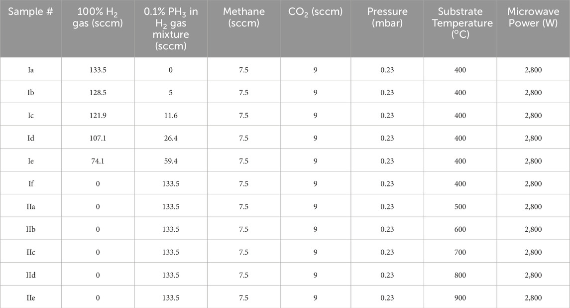
Table 1. Linear antenna microwave plasma CVD diamond deposition conditions (film thickness was kept constant at 250 nm with in-situ laser interferometer monitoring).
2.3 Physical characterisations
AFM was performed in tapping mode to observe the effect of CF4 plasma treatment on substrates and was also used to observe the nanocrystalline diamond (NCD) grains after CVD growth. Scanning electron microscopy (SEM - FEI Quanta 200 FEG) also revealed the as-grown morphology of the diamond films along with the elemental analysis from energy dispersive X-ray spectroscopy (EDS). Raman spectra were recorded with a HORIBA Jobin Yvon T64000 spectrometer using a laser (power 50 mW) light with a wavelength of 488 nm.
3 Results and discussion
3.1 GaN substrate characterisations
Figure 1A is the XRD plot of the as-received GaN on sapphire substrate. It is found to be composed of reflections from (111), (311) and (222) crystal planes which is the signature of face-centred cubic structure (JCPDS file no. 00-052-0791). The XPS results from the plasma treated and untreated surfaces are shown in Figure 1B. CF4-treated substrate has a strong peak corresponding to fluorine 1s. Figure 1B also has peaks other than normal fluorinated or oxygenated GaN surface due to contamination from other elements invariably present inside any sputtering chamber with multiple users (mainly coming from elemental zinc). It has been found that the plasma pre-treatment enhances the nucleation density and produces diamond films without pinholes (Pobedinskas et al., 2013). Such nucleation enhancement happens not only because of fluorination-induced change in surface state but also due to the change in surface roughness, as can be found from the atomic force microscopy (AFM) images of the fluorinated and untreated GaN substrate surfaces, shown in Figure 2. As-received GaN had a very smooth surface (Figure 2A) which is detrimental for mechanical anchoring of the coating, but it is found that CF4 plasma not only incorporates fluorine atoms on the GaN surface but also etches the surface to create planar defects (Figure 2B), helpful in nucleation enhancement of CVD grown diamond. The initial difference in height between asperities and valleys for the untreated GaN surface was 15 nm, which increased to 312.4 nm after 20 s of CF4 plasma pretreatment. The CF4 plasma pre-treatment is not detrimental to the GaN two-dimensional electron gas (2DEG) properties (Pobedinskas et al., 2022). Some additional effects of CF4 plasma treatment will also be discussed in the later sections with Raman spectroscopy results.
Figure 1. GaN substrate characterizations (A) XRD and (B) XPS.

Figure 2. AFM images of (A) untreated and (B) CF4 treated GaN substrate.
3.2 LA MW PE CVD diamond growth chemistry
Figure 3A shows the optical emission spectra (OES) spectra from the diluted phosphine-rich plasma, and Figure 3B shows the OES spectra from pure hydrogen plasma chemistries used during the CVD growth of diamond films on GaN/sapphire substrates. Hα and Hβ are the two most prominent lines at about 655 nm and 485 nm due to the electronic transition from hydrogen atom inner shell 3 to 2 and 4 to 2 respectively [ (Mallik et al., 2014a; Pobedinskas et al., 2014)]. All other spectral lines corresponding to different plasma species (atomic hydrogen = 602 nm, CH = 433 nm, C2 = 580 nm) identical for both pure H2 and diluted PH3 plasma chemistries, are also present in Figure 3. The critical point to be noted is that there is no additional spectral line for diluted phosphine (the amount of P is negligible in these experiments and OES spectrometer is not sensitive enough to detect very low levels of P) plasma than from the pure hydrogen plasma, but the intensities of such spectral lines are higher (IHα 11,928 vs. 10,810, or IHβ 5,272 vs. 4,800) for the diluted phosphine rich gas chemistry than pure hydrogen plasma chemistry during CVD growth of diamond. The absolute intensity variation observed here is more than 10%. Which is typical variation of plasma intensity during the same CVD run [ (Urbach et al., 2023)].
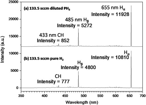
Figure 3. OES of (A) diluted phosphine plasma and (B) pure hydrogen plasma chemistries during CVD diamond growth. Table 1, samples Ia and If, common processing conditions were MW input power 2 × 2800 W, 9 sccm CO2, 7.5 sccm CH4.
3.3 Effect of diluted phosphine (0.1% in H2) gas precursor on low-temperature (400°C) CVD diamond growth: SEM, Raman and EDS
3.3.1 Silicon reference substrates: nanocrystalline diamonds (NCDs)
Figure 4 shows the diamond film morphologies that appeared on the reference Si substrates as the phosphine gas (diluted with H2) was increased gradually in the CVD precursor gas recipe (Table 1, Ia-If). In the beginning, when there was no diluted phosphine in the precursor gas, only pure hydrogen was used as the main precursor ingredient; the average size of the nanocrystalline grains is about 50–150 nm (Figure 4A). With the addition of diluted phosphine gas to the precursor recipe with a 5 sccm flow rate (3.3%), the average NCD grain size becomes bigger, many grains are more than 250 nm (Figure 4B). However, the effect of successive addition of diluted phosphine gas on the average grain sizes of NCDs is not significant and does not follow any trend, as evident from the corresponding morphologies in Figure 4. Wide variation of NCD grain size distribution (as small as 30–40 nm) appeared when 7.7% or 11.6 sccm diluted PH3 (Figure 4C) was present in the precursor gas, whereas the bigger and more uniform NCD grain morphology (150–200 nm) was observed, when the diluted PH3 flow rate was 59.4 sccm (Figure 4E, 39.6%). The respective grains (Figures 4A–E) are irregular in shape and sizes, as typical for nanocrystalline diamond films. But the morphology of the diamond film, when diluted phosphine gas (0.1% PH3 in H2) completely replaced all the pure hydrogen (100% H2) in the precursor recipe with a flow rate of 133.5 sccm (Figure 4F, 89%), is observed to be somewhat different, with elongated (about 190 nm in length and 50 nm in breadth) worm-like grainy appearance. Such morphology is uniformly distributed, unlike the previous ones with lower diluted phosphine gas levels. The possible explanation for getting preferential growth along one lateral direction may be because a linear antenna CVD reactor promotes lateral growth (Drijkoningen et al., 2017) when it is allowed to grow for longer diamond growth periods.
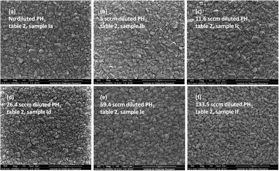
Figure 4. Effect of phosphine gas (0.1% in H2) addition on the diamond film morphologies grown over reference silicon substrates, as evident from their SEM micrographs, from (A–F) with increasing phosphine gas flow rates.
3.3.2 GaN substrates: Etching
Figure 5 shows the effect of phosphine gas (0.1% or 1,000 ppm in H2) addition on the diamond film morphologies and their qualities grown over the GaN/sapphire substrates. It has been reported earlier (May et al., 2006) that under diamond CVD growth conditions the GaN substrate reacts with the hydrogen gas plasma due to harsh environment. But as shown in Figure 5A, the diamond film grown on the GaN surface with 100% pure hydrogen as the main precursor gas does not show any sign of substrate etching. The corresponding Raman signals (Figure 5C) also clearly indicate the presence of microcrystalline diamond (MCD–sp3 peak position 1,332 cm−1) in contrast to NCD morphologies simultaneously observed on the reference Si substrate, Figure 4A. However, it was also observed that substrate etching is prevalent in the case of the samples prepared with the addition of diluted phosphine gas precursor (0.1% PH3 in H2), as shown in Figures 5B, 6. It might be that the phosphine-doping hydrogen plasma conditions were harsher (more reactive species with more energy) than pure 100% hydrogen CVD plasma environment. However, due to natural variation in OES spectra, harsher plasma chemistry cannot be conclusively claimed. Such harsh CVD processing conditions have clearly etched the GaN substrate, as shown in Figures 5B, 6. The corresponding Raman signal (Figure 5D) indicates the presence of both the microcrystalline (1,331.1 cm−1) and nanocrystalline (trans-polyacetylene, 1,140 cm−1 and 1,484 cm−1) diamonds. The magnified peak contours shown for the position 1,332 cm−1 in the insets of Figures 5C, D are significantly different. The sp3 peak for the pure hydrogen precursor sample is sharply present at the theoretical 1,332 cm−1 position (stress free), whereas, for the sample prepared with diluted phosphine gas, the diamond peak is broadened and split into three positions (1,327 cm−1–2.83 GPa tensile, 1,330 cm−1 – 1.13 GPa tensile and 1,335 cm−1–1.7 GPa compressive), indicating smaller grain sizes and anisotropic stress present inside (Mallik et al., 2014b). Diamond on GaN films reportedly (Malakoutian et al., 2019) is associated with thermal stress (due to cooling down after CVD growth) (Cuenca et al., 2021) and intrinsic stress due to the defects (point defects, dislocation, twinning, grain boundary, non-diamond phases, etc.) that appear due to CVD growth. Malakoutian et al. showed that only compressive stresses (−3.4 to −5.2 GPa) were present inside the CVD grown diamond on GaN films with varying CH4 percentages. This was mainly due to the thermal stress that was generated by cooling down diamond film with thermal expansion mismatch with GaN substrate, from the high temperature (600o – 850°C) of CVD growth to room temperature. However, LACVD is a low temperature processing which is unlikely to induce thermal stress with slow cooling. In fact, thermal stress was absent in the film prepared with H2 gas, however, PH3 gas in the recipe etched the substrate surface and produced defects in the diamond-on-GaN films which is evident from the blue shift and red shift of the respective Raman signals from the theoretical sp3 Raman peak position. More evidence of GaN surface etching is also present in their corresponding Raman signatures. The film grown with pure hydrogen plasma shows a crystalline Raman peak of GaN at 571 cm−1 from the base substrate (upshifted and stressed GaN), whereas the Raman signal from the film grown under diluted phosphine plasma chemistry does not have any GaN crystalline peak from the base substrate (range not shown here for better clarity of the graph, but details will be discussed in Section 3.4). The GaN theoretical peak position should have been at 569 cm−1 (E2 mode), and there is also could have been a peak at 578 cm-1 (Eg mode) for the underlying sapphire substrate, as reported before (Azuhata et al., 1995). GaN (and the top diamond film) was thick enough to prevent the Raman laser probe from reaching the underlying sapphire. In addition, there is also the appearance of a Raman peak at 670 cm-1 for the sample prepared with pure hydrogen plasma, which is typical for ion-implanted GaN on sapphire substrates, as previously reported (Kumar et al., 2001). Researchers have suggested that the appearance of a peak at 670 cm−1 is not due to the scattering from the implanted atom but due to the vibrational mode of the host GaN lattice (Limmer et al., 1998). The absence of a GaN Raman peak (full range is not shown in Figure 5D) indicates that CVD plasma conditions under a diluted phosphine environment destroyed the GaN crystal structure, as previously reported by May et al. (May et al., 2006).
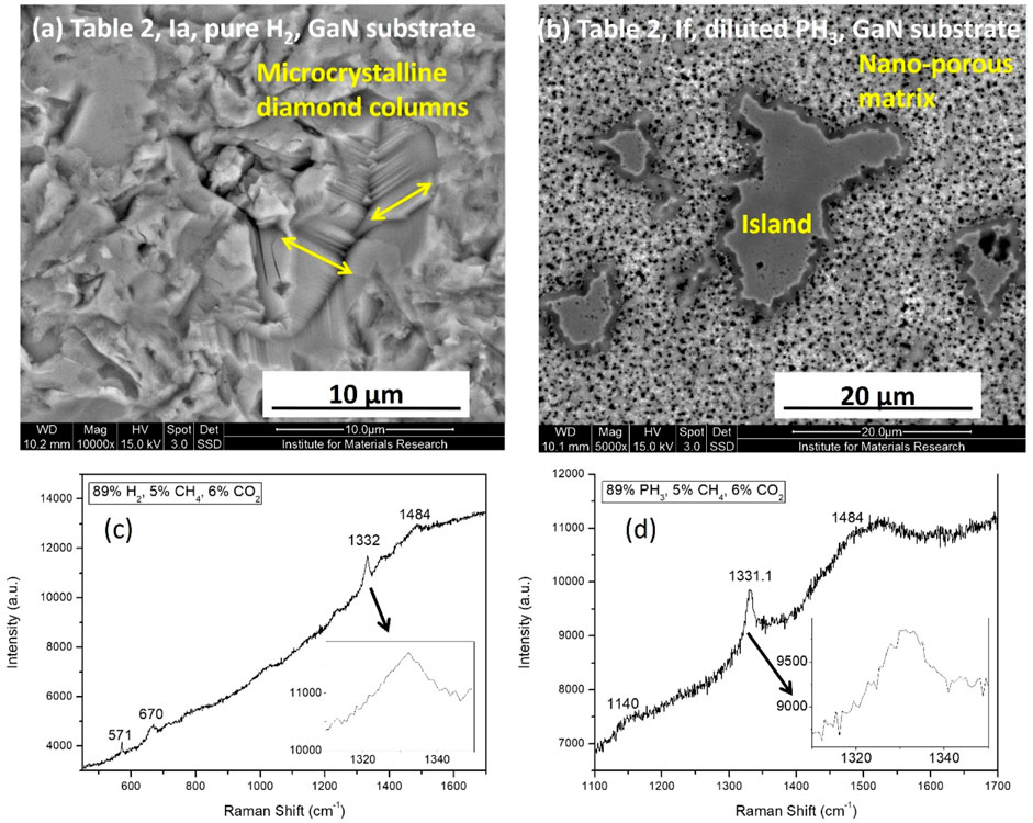
Figure 5. Etching effect of diluted phosphine gas as compared to pure hydrogen precursor gas on the CVD diamond film SEM morphologies (A) pure H2; (B) diluted PH3 (0.1% in H2), grown over GaN substrates and their corresponding Raman spectra (C) pure H2; (D) diluted PH3 (0.1% in H2). Insets are the magnified view of the 1,332 cm-1 diamond peak position for better clarity of peak broadening and splitting.
Etching of GaN surface has already been proposed by May et al. It begins from 600°C which is well below the conventional CVD diamond deposition temperature of 800°C or higher. This work used a low-pressure low-temperature CVD growth environment (Drijkoningen et al., 2017), which did not damage the GaN substrate. But when diluted phosphine gas was used for doping with pure hydrogen in the precursor gas recipe for CVD diamond growth, it resulted in a reaction of the plasma species with GaN surface, even at a lower substrate temperature of 400°C and very low chamber pressure of 0.23 Torr. May et al. proposed that GaN surface reactions caused the nitrogen and ammonia gas to escape through the growing films, thus making the morphology porous. The energy dispersive analysis of X-ray (EDS) signals from the etched GaN surface after diamond deposition is shown in Figure 6. The etched surface has island-like structures distributed in the porous matrix (Figure 5B). The larger pores are big about 0.6 µm in diameter. The islands-like structures are also different in size and shape. The bigger islands are about more than 20 µm in length and about 10 µm in breadth. There are also numerous smaller isolated islands-like structures, as small as 7–8 µm in maximum length. EDS scan over the areas, including the island, shows high-intensity Ga and low-intensity Al elemental peaks coming from the heterostructure substrate, other than a strong elemental C peak coming from the deposited diamond film. The C peak intensity is somewhat reduced when the EDS scan is taken over the areas, including both the island-like structure and the porous matrix. The porous matrix area also resulted in signals from elements like Si, O and N, which are absent from the area scan over the islands. The Al signal is also enhanced from the porous matrix which clearly indicates that the diluted phosphine gas plasma chemistry has severely damaged the GaN surface to expose the underneath sapphire layer. The presence of silicon is due to (a) the presence of the reference Si sample kept alongside the GaN/sapphire substrate during CVD growth of diamond films and, (b) may be a contamination from the linear antenna quartz tubes.
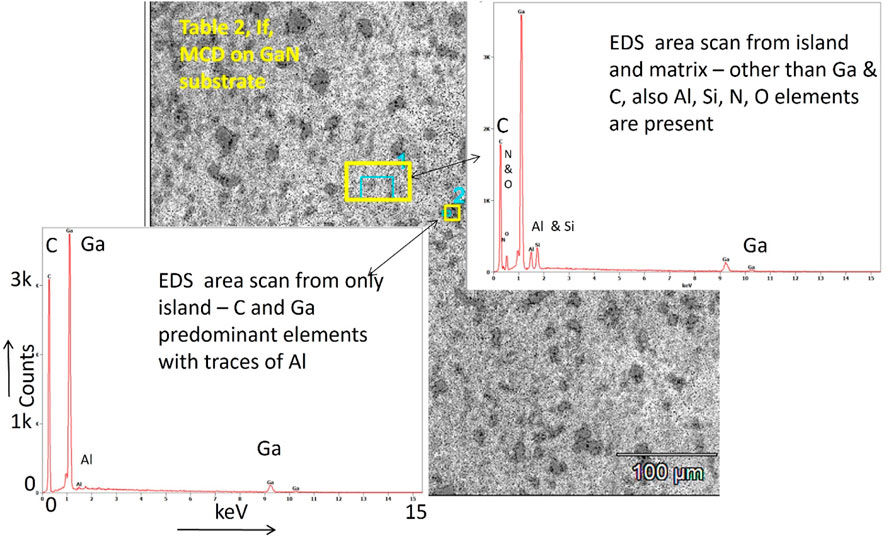
Figure 6. EDS signals indicate GaN substrate etching under CVD diamond deposition conditions when diluted phosphine gas used as the atomic hydrogen source precursor.
3.4 Effect of diluted phosphine gas (0.1% in H2) with increasing substrate temperatures (500°C–900°C)
3.4.1 XPS results
To investigate the effect of diluted phosphine gas addition on the level of phosphorous doping inside the diamond lattice, firsthand conductivity measurements by laboratory electrometer (touching the diamond surface with two probing pins) reveals that the diamond films (Table 1, samples Ia-If) deposited at the lower substrate temperature of 400°C has very high resistance. Figure 7 shows the XPS signals for the diamond films deposited at two relatively different substrate temperatures, 500°C and 900°C respectively (Table 1, samples IIa and IIe). There is a prominent C1s carbon peak (284.3 eV) for both the diamond films, but within the range from 128 eV to 140 eV, there was no sign of incorporation of phosphorous atoms inside the diamond structure synthesized at 500°C, as shown in Figure 7C. On the other hand, after increasing the substrate temperature from 500°C to 900°C the phosphorous atoms were clearly incorporated into the diamond structure, Figure 7B. Deconvolution of the XPS signals from 128 eV to 140 eV binding energy range shows signature peaks corresponding to phosphorous atom 2p3/2 and 2p1/2 electron energy levels for the sample series IIe. Phosphorous has a larger diameter than carbon atoms, so lattice incorporation needs a higher diamond growth temperature to accommodate P atoms (Zhou et al., 2017a; Seelmann-Eggebert et al., 2001; Bland et al., 2019). It is to be noted that, the XPS signals were received from the surface of the CVD-grown diamond films. However, XPS does not reveal the composition from the bulk. Secondary ion mass spectroscopy (SIMS) will be a more appropriate method of determining P doping levels inside the diamond films (Mary Joy et al., 2024). Nevertheless, considering the thin (250 nm) nature of the NCD films grown by LA MW PE CVD, XPS data proves the incorporation of P in the diamond crystal structure, at least confirmatively on the NCD film top layer surface. In the following section, such efforts with diluted phosphine precursor gas and with increasing substrate temperature on the diamond film morphology and quality will be presented and discussed.
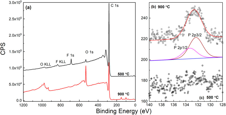
Figure 7. XPS signals (A) for the samples grown at 500°C (IIa) and 900°C (IIe); (B) corresponding deconvolution of the spectra from 140 to 128eV binding energy - indicate incorporation of phosphorous only in the NCD film deposited at 900°C substrate temperature with diluted PH3 (0.1% in H2) CVD precursor gas.
3.4.2 AFM and SEM results
AFM image (Figure 8) of the NCD grains deposited at a higher substrate temperature of 800°C (sample IId) shows a slightly smaller and smoother film compared to the NCD grown at 500°C (sample IIa) when diluted phosphine was the main precursor gas (Table 1). The triangular-shaped grains indicate prevalent (111) faceted morphologies. The AFM image also reveals a porous NCD structure, which is further confirmed by the SEM images in Figure 9 – which shows the effect of the successive rise of substrate temperatures at 600°C (Figure 9A), 700°C (Figure 9B), 800°C (Figure 9C) and 900°C (Figure 9D) on diamond morphologies. The microstructure shown in Figure 9C is from the same sample shown in Figure 8B (sample IId), which also validates the fact that the NCDs grown at higher temperatures have smaller grain sizes (250–300 nm) than NCDs grown at lower temperatures (600°C–Figure 9A, sample IIb, average sizes 400–500 nm). Although the diamond sample (IIe) deposited at 900°C substrate temperature, shown in Figure 9D, does not (300–400 nm) show the smallest grain size of them all. Therefore, it can be inferred that NCD grain size does not follow a definitive trend with increasing substrate temperature, but they are all fully covered substrates without the evidence of any GaN substrate etching, in contrast to the earlier findings in their SEM microstructure grown at a low temperature of 400°C (Figures 5B, 6). The reason for not showing substrate surface etching at higher temperatures is counterintuitive. The logic behind substrate etching by the earlier report (May et al., 2006) was that at high temperature GaN reacts with the hydrogen gas. By using a lower substrate temperature inside the linear antenna system, substrate etching could be avoided, while using hydrogen as the precursor gas. However, when diluted phosphine was added to the gas mixture recipe, it was found to, etch the GaN substrate, even at low substrate temperature. Surprisingly, the GaN substrate etching disappears as we increase the substrate temperature from 400°C to 900°C. The heater underneath the substrate stage heated up the samples. Such additional thermal energy might have helped the substrate surface reactant species to become mobile and cover up the GaN substrate fully with a growing diamond before the plasma damages the GaN crystals. It is to be noted that the linear antenna CVD reactor promotes lateral growth of the diamond crystals (Mallik et al., 2024; Drijkoningen et al., 2017). Figure 9 show that the diamond crystals are 250 nm–500 nm in sizes, while the NCD film thickness on Si reference substrate was restricted to 250 nm only during the experiments. Therefore, such preferential lateral growth of diamond helped in achieving quick surface coverage, leading to the protection of the underlying GaN substrate from CVD plasma etching.
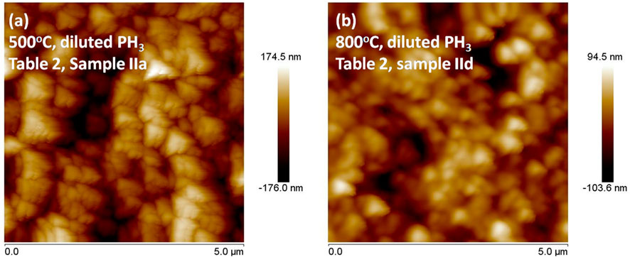
Figure 8. AFM images of the nanocrystalline diamond (NCD) films grown on GaN substrates with diluted phosphine (0.1% PH3+99.9% H2 gas mixture) at different substrate temperatures (A) 500°C, (B) 800°C.
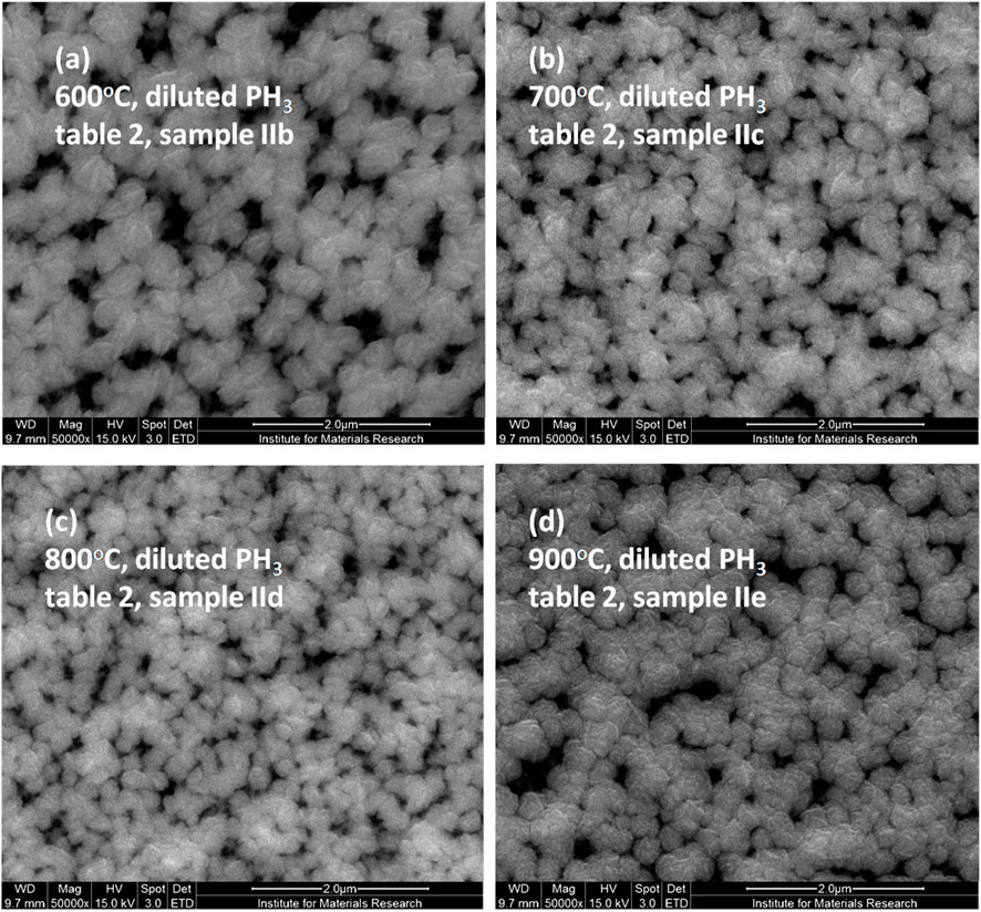
Figure 9. Effect of substrate temperature (A) 600o, (B) 700o, (C) 800o, (D) 900°C, on the CVD diamond film morphologies, deposited onto GaN substrate with diluted phosphine (0.1% in H2) as precursor gas, as evident from SEM images.
It could be that the etched GaN releases N which accelerates the NCD growth. The nature of the film surface indicates that the GaN crystal reacted with the plasma species, which made the reaction gas products to escape through the film, thus making the film porous. Figure 9A morphology is found to be more porous than Figure 9D, which is believed to be due to more GaN decomposition/chemical reactions at lower substrate temperatures than the favorable formation of diamond film at increasing substrate temperatures. At the lower substrate temperature, due to less coverage of the GaN surface by the growing diamond film, the substrate was exposed long enough time to the CVD plasma to cause damage to the GaN material.
3.4.3 Raman results
Such relative competition between GaN decomposition and diamond film formation, is also evident from the gradual appearance of Raman signals, arising from the undamaged substrate surface with increasing substrate temperature, as presented in Figure 10. The appearance of peak at 569 cm−1 is due to E2 mode optical phonon and 735 cm−1 signal is due to A1(LO) mode for GaN crystal grown over sapphire substrates (Azuhata et al., 1995). The GaN Raman signals from the film grown at 900°C (Figure 10D) is the most prominent as compared to the signals from the films deposited at 700°C and 800°C, whereas the film grown at 600°C does not show any Raman signal (Figure 10A) from the underneath substrate. The corresponding diamond film Raman peaks typically are present in and around 1,140, 1,332 and 1,480 cm−1, due to the presence of trans-polyacetylene (TPA), sp3 phases and amorphous carbon respectively. There is a significant peak broadening beyond the theoretical sp3 peak position for the film (sample IIe) grown at the highest substrate temperature of 900°C. The upshift corresponds to huge amount of compressive stress (Mallik et al., 2014b) present inside the diamond lattice. It is because that at the 900°C of substrate temperature, the phosphorous atoms are incorporated inside the diamond films. The size of phosphorous atoms being larger than the carbon atom, P atom squeezes the diamond cubic lattice into compressive pressure. The gradual appearance of GaN Raman signals with an increase in substrate temperature is an indication of the favorable laser light interaction from the undamaged GaN surface. It has been described that the growing film thickness on Si substrate has been kept constant at 250 nm by monitoring the in-situ laser interferometer signals during CVD growth (Table 1). If it is assumed that the film thickness is equal for all the deposited film, then, the stronger substrate signals imply additional heating by substrate heater helped in protecting the bare GaN substrate from harsh diluted phosphine plasma CVD environment by fully covering the surface with NCD films. May et al. (2006) elaborately described how the competition between GaN substrate decomposition and diamond film deposition at high substrate temperatures determines the ultimate film quality. They showed that at 800°C high temperatures, GaN crystallinity is destroyed completely and could not produce any Raman peak. Moreover, the Raman peak at 569 cm-1 corresponding to E2 mode was not detected. Here it was found that not only two Raman peaks for GaN, but contrary to their earlier report, it is also observed that the GaN peaks are getting prominent with increasing substrate temperature. So, it can be inferred that temperature is not the only determining factor in GaN substrate etching. It is more important to have correct CVD plasma conditions (diluted PH3) conducive to diamond growth. Figure 10A has no GaN Raman peak, which is processed (sample IIb) at a relatively lower temperature of 600°C. It indicates that the GaN decomposition rate is high enough compared to the diamond film formation. Still, as the substrate temperature is increased further from 700o to 900°C, there is a gradual decrease in the GaN decomposition rate, as evident from the gradual appearance of the GaN Raman peaks (inset of Figure 10). So, it is concluded that the increase in substrate temperature favors diamond growth and suppresses GaN substrate decomposition. The favorable high CVD substrate temperature helped the diamond film to form quickly over the GaN substrate, thus not letting the corrosive plasma species like atomic hydrogen (Hα and Hβ) come in direct contact with the GaN substrate surfaces to cause chemical reactions or etching. Diamond crystals grow both in the vertical columns and horizontal planar direction. Quick substrate surface coverage with growing diamond layer is essential to prevent etching of GaN. Since LACVD reactor favors lateral growth over columnar growth, GaN etching is further prevented inside this type of reactor.
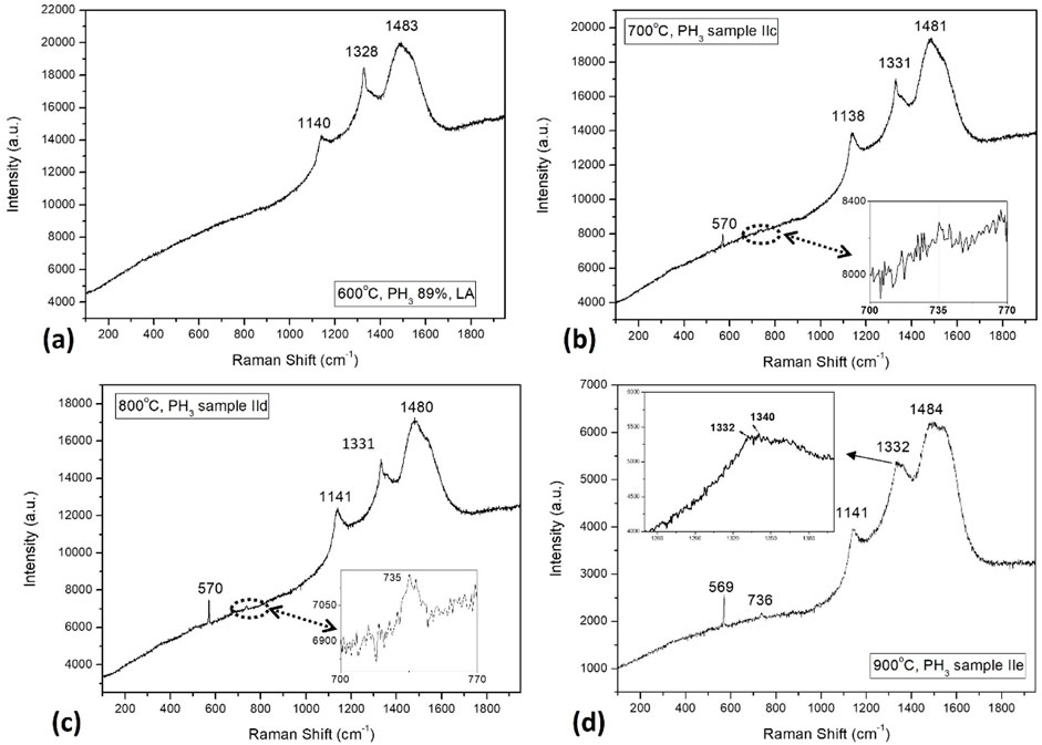
Figure 10. Effect of substrate temperatures on the Raman spectra of the NCDs grown over GaN substrates with diluted PH3 (0.1% in H2) precursor gas, (A) 600°C, (B) 700°C, (C) 800°C and (D) 900°C.
4 Conclusion
Microcrystalline and nanocrystalline diamond films were deposited on GaN/sapphire heterostructure substrates with hydrogen as precursor gas without causing any apparent substrate surface etching, as previously reported in the literature. It was also possible to avoid having any SiN barrier layer between the diamond and GaN/sapphire substrate, which is different from the routine practice by other researchers. Three essential research problems were addressed using a linear antenna microwave plasma-enhanced CVD system to grow diamonds at a very low substrate temperature of 400°C. However, such low-temperature CVD growth conditions were found to, etch the GaN substrate when diluted phosphine gas was used as a doping precursor. Phosphine precursor gas could not render room-temperature conductivity to the growing diamond films. The highly resistive diamond film deposition was due to the low substrate temperature of 400°C, which was not high enough to incorporate phosphorous atoms inside the diamond lattice. Therefore, low CVD growth temperature not only etched the GaN surface but was also futile in doping the diamond film. However, when higher substrate temperatures were adopted, then it was found that a substrate temperature of 900°C could achieve phosphorous doping. Unfortunately, higher substrate temperatures (600o-900°C) made the diamond film porous. Contrary to the earlier literature reports, this work finds that higher substrate temperatures do not damage the GaN/sapphire substrates due to favorable conditions of CVD diamond lateral growth in competition over the underneath GaN substrate decomposition in the linear antenna CVD reactor. On the other hand, lower substrate temperature accelerated GaN decomposition, by not letting diamond film form faster enough to cover the substrate, when diluted phosphine was used as the precursor gas.
The objectives of the paper were: (A) direct CVD growth of diamond at lower temperatures to address the problem of GaN substrate etching, by growing diamond on the GaN/sapphire heterostructures without a silicon nitride layer on top of the substrates and, (B) to study the effect of such a new PH3-based precursor recipe on the diamond films grown over the GaN/sapphire substrate heterostructure. The results show that the research objectives are well met. Further work is necessary to fully characterize the respective thermal (conductivity and TBR) and electrical (2DEG) properties, which is out of scope of the present work.
Author contributions
AM: Conceptualization, Data curation, Formal Analysis, Investigation, Methodology, Resources, Software, Validation, Visualization, Writing–original draft, Writing–review and editing. KS: Conceptualization, Data curation, Formal Analysis, Methodology, Resources, Validation, Visualization, Writing–review and editing. DD: Data curation, Formal Analysis, Investigation, Methodology, Resources, Writing–review and editing. PP: Conceptualization, Data curation, Formal Analysis, Investigation, Methodology, Resources, Validation, Visualization, Writing–review and editing. RJ: Data curation, Investigation, Methodology, Resources, Writing–review and editing. RR: Conceptualization, Data curation, Formal Analysis, Investigation, Methodology, Resources, Validation, Visualization, Writing–review and editing. FL: Conceptualization, Data curation, Formal Analysis, Investigation, Methodology, Resources, Validation, Visualization, Writing–review and editing. H-GB: Funding acquisition, Project administration, Supervision, Validation, Writing–review and editing. KH: Funding acquisition, Investigation, Project administration, Resources, Supervision, Validation, Writing–review and editing.
Funding
The author(s) declare that financial support was received for the research, authorship, and/or publication of this article. This work was financially supported by the Methusalem NANO network and the Research Foundation – Flanders (FWO) via project G0D4920N. AKM acknowledges FWO for his Postdoctoral Fellowship with grant no. 12X2919N.
Acknowledgments
Johnny Baccus and Christel Willems supported experimental planning and execution. AKM and PP acknowledge the Research Foundation–Flanders (FWO) for a postdoctoral fellowship. All data generated or analysed during this study are included in this published article. The datasets generated during and/or analysed during the current study are available from the corresponding author upon reasonable request.
Conflict of interest
The authors declare that the research was conducted in the absence of any commercial or financial relationships that could be construed as a potential conflict of interest.
Publisher’s note
All claims expressed in this article are solely those of the authors and do not necessarily represent those of their affiliated organizations, or those of the publisher, the editors and the reviewers. Any product that may be evaluated in this article, or claim that may be made by its manufacturer, is not guaranteed or endorsed by the publisher.
References
Anaya, J., Rossi, S., Alomari, M., Kohn, E., Toth, L., Pecz, B., et al. (2016). Control of the in-plane thermal conductivity of ultra-thin nanocrystalline diamond films through the grain and grain boundary properties. Acta Mater. 103, 141–152. doi:10.1016/j.actamat.2015.09.045
Azuhata, T., Sota, T., Suzuki, K., and Nakamura, S. (1995). Polarized Raman spectra in GaN. J. Phys. Condens. Matter 7, L129–L133. doi:10.1088/0953-8984/7/10/002
Bland, H. A., Thomas, E. L. H., Klemencic, G. M., Mandal, S., Morgan, D. J., Papageorgiou, A., et al. (2019). Superconducting diamond on silicon nitride for device applications. Sci. Rep. 9, 2911–2919. doi:10.1038/s41598-019-39707-z
Cuenca, J. A., Smith, M. D., Field, D. E., Massabuau, F. C.-P., Mandal, S., Pomeroy, J., et al. (2021). Thermal stress modelling of diamond on GaN/III-Nitride membranes. Carbon 174, 647–661. doi:10.1016/j.carbon.2020.11.067
Das, D., and Singh, R. N. (2007). A review of nucleation, growth and low temperature synthesis of diamond thin films. Int. Mater. Rev. 52, 29–64. doi:10.1179/174328007x160245
Degutis, G., Pobedinskas, P., Boyen, H.-G., Dexters, W., Janssen, W., Drijkoningen, S., et al. (2015). Improved nanodiamond seeding on chromium by surface plasma pretreatment. Chem. Phys. Lett. 640, 50–54. doi:10.1016/j.cplett.2015.10.002
Domonkosa, M., Ižák, T., Varga, M., Potocký, Š., Demo, P., and Kromka, A. (2018). Diamond nucleation and growth on horizontally and vertically aligned Si substrates at low pressure in a linear antenna microwave plasma system. Diam. and Relat. Mater. 82, 41–49. doi:10.1016/j.diamond.2017.12.018
Drijkoningen, S., Pobedinskas, P., Korneychuk, S., Momot, A., Balasubramaniam, Y., Van Bael, M. K., et al. (2017). On the origin of diamond plates deposited at low temperature. Cryst. Growth and Des. 17, 4306–4314. doi:10.1021/acs.cgd.7b00623
Ejeckam, F., Babic, D., Faili, F., Francis, D., Lowe, F., Diduck, Q., et al. (2014). 3,000+ hours continuous operation of GaN-on-Diamond HEMTs at 350C channel temperature, semiconductor thermal measurement and management symposium (SEMI-THERM). 30th Annu. doi:10.1109/SEMI-THERM.2014.6892247
Ficek, M., Niedziałkowski, P., Śmietana, M., Koba, M., Drijkoningen, S., Bogdanowicz, R., et al. (2017). Linear antenna microwave chemical vapour deposition of diamond films on long-period fiber gratings for bio-sensing applications. Opt. Mater. Express 7, 3952. doi:10.1364/ome.7.003952
Field, D. E., Cuenca, J. A., Smith, M., Fairclough, S. M., Massabuau, F. C.-P., Pomeroy, J. W., et al. (2020). Crystalline interlayers for reducing the effective thermal boundary resistance in GaN-on-Diamond. ACS Appl. Mater. and Interfaces 12 (48), 54138–54145. doi:10.1021/acsami.0c10129
Francis, D., Faili, F., Babić, D., Ejeckam, F., Nurmikko, A., and Maris, H. (2010). Formation and characterization of 4-inch GaN-on-diamond substrates. Diam. Relat. Mater. 19, 229–233. doi:10.1016/j.diamond.2009.08.017
Francis, D., and Kuball, M., 14 - GaN-on-diamond materials and device technology: a review, Editor(s): M. J. Tadjer, and T. J. Anderson, In Woodhead publishing series in electronic and optical materials, thermal management of gallium nitride electronics, Woodhead Publishing, China, 2022, 295–331. doi:10.1016/B978-0-12-821084-0.00006-8
Goyal, V., Sumant, A. V., Teweldebrhan, D., and Balandin, A. A. (2012). Direct low-temperature integration of nanocrystalline diamond with GaN substrates for improved thermal management of high-power electronics. Adv. Funct. Mater. 22, 1525–1530. doi:10.1002/adfm.201102786
Gracio, J. J., Fan, Q. H., and Madaleno, J. C. (2010). Diamond growth by chemical vapour deposition. J. Phys. D Appl. Phys. 43 (37), 374017. doi:10.1088/0022-3727/43/37/374017
Gu, Y., Zhang, Y., Hua, B., Ni, X., Fan, Q., and Gu, X. (2021). Interface engineering enabling next generation GaN-on-Diamond power devices. J. Elec Materi 50, 4239–4249. doi:10.1007/s11664-021-09011-6
Heidger, S. L., Rotter, S. Z., Gillespie, J., and Weimer, J. A. (2004). “High power and high temperature applications of CVD diamond,” in IMAPS International High Temperature Electronics Conference, HiTEC 2004, Santa Fe, NM, 2003-12-05.
Kato, H., Futako, W., Yamasaki, S., and Okushi, H. (2005). Growth of phosphorus-doped diamond using tertiarybutylphosphine and trimethylphosphine as dopant gases. Diam. and Relat. Mater. 14, 340–343. doi:10.1016/j.diamond.2004.11.032
Kato, H., Takeuchi, D., Ogura, M., Yamada, T., Kataoka, M., Kimura, Y., et al. (2016). Heavily phosphorus-doped nano-crystalline diamond electrode for thermionic emission application. Diam. and Relat. Mater. 63, 165–168. doi:10.1016/j.diamond.2015.08.002
Kromka, A., Potocký, Š., Čermák, J., Rezek, B., Potměši, J., Zemek, J., et al. (2008). Early stage of diamond growth at low temperature. Diam. and Relat. Mater. 17, 1252–1255. doi:10.1016/j.diamond.2008.03.035
Kumar, M. S., Kesavamoorthy, R., Magudapathy, P., Nair, K. G. M., and Kumar, J. (2001). Raman scattering studies on hydrogen ion-implanted GaN. Nucl. Instrum. Methods Phys. Res. B 179, 193–199. doi:10.1016/S0168-583X(01)00445-1
Limmer, W., Ritter, W., Sauer, R., Mensching, B., Liu, C., and Rauschenbach, B. (1998). Raman scattering in ion-implanted GaN. Appl. Phys. Lett. 72, 2589–2591. doi:10.1063/1.121426
Liu, D., Francis, D., Faili, F., Middleton, C., Anaya, J., Pomeroy, J. W., et al. (2017). Impact of diamond seeding on the microstructural properties and thermal stability of GaN-on-diamond wafers for high-power electronic devices. Scr. Mater. 128, 57–60. doi:10.1016/j.scriptamat.2016.10.006
Lloret, F., Sankaran, K. J., Millan-Barba, J., Desta, D., Rouzbahani, R., Pobedinskas, P., et al. (2020). Improved Field electron emission properties of phosphorus and nitrogen Co-doped nanocrystalline diamond films. Nanomaterials 10, 1024. doi:10.3390/nano10061024
Malakoutian, M., Field, D. E., Hines, N. J., Pasayat, S., Graham, S., Kuball, M., et al. (2021). Record-low thermal boundary resistance between diamond and GaN-on-SiC for enabling radiofrequency device cooling. ACS Appl. Mater. and Interfaces 13 (50), 60553–60560. doi:10.1021/acsami.1c13833
Malakoutian, M., Laurent, M. A., and Chowdhury, S. (2019). A study on the growth window of polycrystalline diamond on Si3N4-coated N-polar GaN. Crystals 9, 498. doi:10.3390/cryst9100498
Malakoutian, M., Zheng, X., Woo, K., Soman, R., Kasperovich, A., Pomeroy, J., et al. (2022). Low thermal budget growth of near-isotropic diamond grains for heat spreading in semiconductor devices. Adv. Funct. Mater. 32, 2208997. doi:10.1002/adfm.202208997
Mallik, A. K., Bysakh, S., Dutta, S., and Basu, D. (2014a). Correlation between optical emission spectra and the process parameters of a 915 MHz microwave plasma CVD reactor used for depositing polycrystalline diamond coatings. Sadhana 39, 957–970. doi:10.1007/s12046-014-0265-2
Mallik, A. K., Bysakh, S., Sreemany, M., Roy, S., Ghosh, J., Roy, S., et al. (2014b). Property mapping of polycrystalline diamond coatings over large area. J. Adv. Ceram. 3, 56–70. doi:10.1007/s40145-014-0093-1
Mallik, A. K., Lloret, F., Gutierrez, M., Rouzbahani, R., Pobedinskas, P., Shih, W.-C., et al. (2023). Deposition and characterisation of a diamond/Ti/diamond multilayer structure. Coatings 13, 1914. doi:10.3390/coatings13111914
Mallik, A. K., Shih, W. C., Pobedinskas, P., and Haenen, K. (2024). Early periods of low-temperature linear antenna CVD nucleation and growth study of nanocrystalline diamond films. Coatings 14, 184. doi:10.3390/coatings14020184
Mandal, S., Thomas, E. L. H., Middleton, C., Gines, L., Griffiths, J. T., Kappers, M. J., et al. (2017). Surface zeta potential and diamond seeding on gallium nitride films. ACS Omega 2, 7275–7280. doi:10.1021/acsomega.7b01069
Mandal, S. (2021). Nucleation of diamond films on heterogeneous substrates: a review. RSC Adv. 11 (17), 10159–10182. doi:10.1039/d1ra00397f
Mary Joy, R., Pobedinskas, P., Baule, N., Bai, S., Jannis, D., Gauquelin, N., et al. (2024). The effect of microstructure and film composition on the mechanical properties of linear antenna CVD diamond thin films. Acta Mater. 264, 119548. 1359-6454. doi:10.1016/j.actamat.2023.119548
May, P. W., Tsai, H. Y., Wang, W. N., and Smith, J. A. (2006). Deposition of CVD diamond onto GaN. Diam. and Relat. Mater. 15, 526–530. doi:10.1016/j.diamond.2005.11.036
Mendes, J. C., Liehr, M., and Li, C. (2022). Diamond/GaN HEMTs: where from and where to? Mater. (Basel) 15 (2), 415. PMID: 35057131; PMCID: PMC8778208. doi:10.3390/ma15020415
Millán-Barba, J., Taylor, A., Bakkali, H., Alcantara, R., Lloret, F., Guzmán de Villoria, R., et al. (2023). Low temperature growth of nanocrystalline diamond: insight thermal property. Diam. Relat. Mater. 137, 110070. 0925-9635. doi:10.1016/j.diamond.2023.110070
Mohapatra, D. R., Rai, P., Misra, A., Tyagi, P. K., Yadav, B. S., and Misra, D. S. (2008). Parameter window of diamond growth on GaN films by microwave plasma chemical vapor deposition. Diam. Relat. Mater. 17, 1775–1779. doi:10.1016/j.diamond.2008.02.011
Mu, F., Xu, B., Wang, X., Gao, R., Huang, S., Wei, Ke, et al. (2022). A novel strategy for GaN-on-diamond device with a high thermal boundary conductance. J. Alloys Compd. 905, 164076. doi:10.1016/j.jallcom.2022.164076
Mukuda, Y., Watanabe, T., Ueda, A., Nishibayashi, Y., and Einaga, Y. (2015). Electrochemical properties of phosphorus doped diamond. Electrochimica Acta 179, 599–603. doi:10.1016/j.electacta.2015.03.033
Nose, K., Suwa, T., Fujita, R., Kamiko, M., and Mitsuda, Y. (2012). Crystallinity and electrical conductivity of sulfur-containing microcrystalline diamond thin film. Thin Solid Films 520, 4310–4313. doi:10.1016/j.tsf.2012.02.083
Oba, M., and Sugino, T. (2001). Oriented growth of diamond on (0001) surface of hexagonal GaN. Diam. Relat. Mater. 10, 1343–1346. doi:10.1016/s0925-9635(00)00448-9
Piazza, F., and Morell, G. (2007). Synthesis of diamond at sub 300 °C substrate temperature. Diam. and Relat. Mater. 16, 1950–1957. doi:10.1016/j.diamond.2007.08.038
Pobedinskas, P., Degutis, G., Dexters, W., D’Haen, J., Van Bael, M. K., and Haenen, K. (2021). Nanodiamond seeding on plasma-treated tantalum thin films and the role of surface contamination. Appl. Surf. Sci. 538 (2021), 148016. doi:10.1016/j.apsusc.2020.148016
Pobedinskas, P., Degutis, G., Dexters, W., Hardy, A., Van Bael, M. K., and Haenen, K. (2014). Influence of hydrogen and hydrogen/methane plasmas on AlN thin films. Appl. Phys. Lett. 104, 081917. doi:10.1063/1.4867022
Pobedinskas, P., Degutis, G., Dexters, W., Janssen, W., Janssens, S. D., Conings, B., et al. (2013). Surface plasmapretreatment for enhanced diamond nucleation on AlN. Appl. Phys. Lett. 102, 201609. doi:10.1063/1.4807591
Pobedinskas, P., Ramaneti, R., and Haenen, K., Structures and method for growing diamond layers, 348,858 B2, 2022.
Sang, L. (2021) Diamond as the heat spreader for the thermal dissipation of GaN-based electronic devices, 1:1, 174–188. doi:10.1080/26941112.2021.1980356
Schwander, M., and Partes, K. (2011). A review of diamond synthesis by CVD processes. Diam. and Relat. Mater. 20, 1287–1301. doi:10.1016/j.diamond.2011.08.005
Sedov, V., Martyanov, A., Savin, S., Bolshakovc, A., Bushuev, E., Khomich, A., et al. (2018). Growth of polycrystalline and single-crystal CVD diamonds with bright photoluminescence of Ge-V color centers using germane GeH4 as the dopant source. Diam. and Relat. Mater. 90, 47–53. doi:10.1016/j.diamond.2018.10.001
Seelmann-Eggebert, M., Meisen, P., Schaudel, F., Koidl, P., Vescan, A., and Leier, H. (2001). Heat-spreading diamond films for GaN-based high-power transistor devices. Diam. Relat. Mater. 10, 744–749. doi:10.1016/s0925-9635(00)00562-8
Siddique, A., Ahmed, R., Anderson, J., Nazari, M., Yates, L., Graham, S., et al. (2019). Structure and interface analysis of diamond on an AlGaN/GaN HEMT utilizing an in situ SiNx interlayer grown by MOCVD. ACS Appl. Electron. Mater. 1, 1387–1399. doi:10.1021/acsaelm.9b00131
Simon, R. B., Anaya, J., Faili, F., Balmer, R., Williams, G. T., Twitchen, D. J., et al. (2016). Effect of grain size of polycrystalline diamond on its heat spreading properties. Appl. Phys. Express 9, 061302. doi:10.7567/apex.9.061302
Soga, T., Sharda, T., and Jimbo, T. (2004). Precursors for CVD growth of nanocrystalline diamond. Phys. Solid State 46, 720–725. doi:10.1134/1.1711458
Sternschulte, H., Schreck, M., Stritzker, B., Bergmaier, A., and Dollinger, G. (2003). Growth and properties of CVD diamond films grown under H2S addition. Diam. Relat. Mater. 12, 318–323. doi:10.1016/s0925-9635(02)00312-6
Sun, H., Simon, R. B., Pomeroy, J. W., Francis, D., Faili, F., Twitchen, D. J., et al. (2015). Reducing GaN-on-diamond interfacial thermal resistance for high power transistor applications. Appl. Phys. Lett. 106, 111906. doi:10.1063/1.4913430
Truscott, B. S., Kelly, M. W., Potter, K. J., Ashfold, M. N. R., and Mankelevich, Y. A. (2016). Microwave plasma-activated chemical vapor deposition of nitrogen-doped diamond. II: CH4/N2/H2 plasmas. J. Phys. Chem. A 120, 8537–8549. doi:10.1021/acs.jpca.6b09009
Urbach, J. P., Schütte, T., Ahmed, E., Pobedinskas, P., and Haenen, K. (2023). Enabling automated process control by simultaneous in-situ measurement of plasma process and thin film growth in real-time. 66th Annu. Tech. Conf. Proc. doi:10.14332/svc23.proc.0048
Waller, W. M., Pomeroy, J. W., Field, D., Smith, E. J. W., May, P. W., and Kuball, M. (2020). Thermal boundary resistance of direct van der Waals bonded GaN-on-diamond. Semicond. Sci. Technol. 35 (9), 095021. doi:10.1088/1361-6641/ab9d35
Wang, A., Tadjer, M. J., and Calle, F. (2013). Simulation of thermal management in AlGaN/GaN HEMTs with integrated diamond heat spreaders. Semicond. Sci. Technol. 28, 055010. doi:10.1088/0268-1242/28/5/055010
Weng, J., Liu, F., Xiong, L. W., Wang, J. H., and Sun, Q. (2018). Deposition of large area uniform diamond films by microwave plasma CVD. Vacuum 147, 134–142. doi:10.1016/j.vacuum.2017.10.026
Williams, O. A., Douheret, O., Daenen, M., Haenen, K., Osawa, E., and Takahashi, M. (2007). Enhanced diamond nucleation on monodispersed nanocrystalline diamond. Chem. Phys. Lett. 445, 255–258. doi:10.1016/j.cplett.2007.07.091
Woo, K., Malakoutian, M., Jo, Y., Zheng, X., Pfeifer, T., Mandia, R., et al. (2023). Interlayer engineering to achieve <1 m2K/GW thermal boundary resistances to diamond for effective device cooling. 2023 Int. Electron Devices Meet. (IEDM), 1–4. doi:10.1109/IEDM45741.2023.10413734
Yates, L., Anderson, J., Gu, X., Lee, C., Bai, T., Mecklenburg, M., et al. (2018). Low thermal boundary resistance interfaces for GaN-on-Diamond devices. ACS Appl. Mater. Interfaces 10, 24302–24309. doi:10.1021/acsami.8b07014
Zhan, T., Xu, M., Cao, Z., Zheng, C., Kurita, H., Narita, F., et al. (2023). Effects of thermal boundary resistance on thermal management of gallium-nitride-based semiconductor devices: a review. Micromachines 14, 2076. doi:10.3390/mi14112076
Zhang, Y., Dadgar, A., and Palacios, T. (2018). Gallium nitride vertical power devices on foreign substrates: a review and outlook. J. Phys. D. Appl. Phys. 51, 273001. doi:10.1088/1361-6463/aac8aa
Zhou, Y., Anaya, J., Pomeroy, J., Sun, H., Gu, X., Xie, A., et al. (2017a). Barrier-layer optimization for enhanced GaN-on-Diamond device cooling. ACS Appl. Mater. and Interfaces 9, 34416–34422. doi:10.1021/acsami.7b08961
Zhou, Y., Ramaneti, R., Anaya, J., Korneychuk, S., Derluyn, J., Sun, H., et al. (2017b). Thermal characterization of polycrystalline diamond thin film heat spreaders grown on GaN HEMTs. Appl. Phys. Lett. 111, 041901. doi:10.1063/1.4995407
Keywords: diamond, GaN, chemical vapor deposition, phosphine, hydrogen, etching
Citation: Mallik AK, Sankaran KJ, Desta D, Pobedinskas P, Joy RM, Rouzbahani R, Lloret F, Boyen H-G and Haenen K (2025) LACVD growth of diamond on gallium nitride substrates with PH3 in recipe. Front. Energy Res. 12:1413495. doi: 10.3389/fenrg.2024.1413495
Received: 07 April 2024; Accepted: 31 October 2024;
Published: 24 February 2025.
Edited by:
Srabanti Chowdhury, Stanford University, United StatesReviewed by:
Bing Dai, Harbin Institute of Technology, ChinaMohamadali Malakoutian, Stanford University, United States
Copyright © 2025 Mallik, Sankaran, Desta, Pobedinskas, Joy, Rouzbahani, Lloret, Boyen and Haenen. This is an open-access article distributed under the terms of the Creative Commons Attribution License (CC BY). The use, distribution or reproduction in other forums is permitted, provided the original author(s) and the copyright owner(s) are credited and that the original publication in this journal is cited, in accordance with accepted academic practice. No use, distribution or reproduction is permitted which does not comply with these terms.
*Correspondence: Awadesh Kumar Mallik, YXdhZGVzaC5tYWxsaWtAZ21haWwuY29t, YXdhZGVzaC5tYWxsaWtAbnR1LmVkdS5zZw==