 X. M. Song
 C. Y. Ye
 Z. G. Huang
95% of researchers rate our articles as excellent or good
Learn more about the work of our research integrity team to safeguard the quality of each article we publish.
Find out more
ORIGINAL RESEARCH article
Front. Energy Res. , 14 November 2023
Sec. Solar Energy
Volume 11 - 2023 | https://doi.org/10.3389/fenrg.2023.1283196
This article is part of the Research Topic The Use of Optimization Techniques in Solar Energy View all 3 articles
Due to the simple process, low energy consumption and stable performance, semiconductor/insulating layer/semiconductor (SIS) solar cells have attracted lots of research interests. However, the device physics of SIS solar cells needs further clarification and improvement. In this paper, the effects of TCO work function on the performance of TCO/SiO2/n-Si heterojunction solar cells were simulated by AFORS-HET and the physics mechanisms for these effects were clarified. It is found that for a work function of 5.2 eV or higher of TCO, the SIS devices possess high ƞ of 22.9% or higher, while the devices show the S-shape J-V curve with low FF when the work function work function of TCO is under 5.1 eV. Further analysis indicates that the work function difference between TCO and n-Si substrate is so small that there is an insufficient band bending at the interface leading to a lower built-in electric field that degrades the photogenerated carriers’ separation, which results in the deformation of J-V curve. Moreover, the simulation results show that the performances of TCO/SiOx/n-Si devices are significantly affected by the band offsets at the SiOx/n-Si interface. When the conduction band offset is higher than 0.4 eV, it can effectively prevent electrons from passing through the SiOx layer to reduce the recombination at the interface, resulting in the excellent output performances of the SIS device. But for a low conduction band order of 0.4 eV or less, the blocking effect of electrons weakens, leading to the large recombination at the interface. Finally, we propose two mechanisms of S-shape J-V curve of SIS solar cells: one is the built-in electric field is too small to separate photogenerated carriers, and the other one is that the carrier transmission is blocked by the thick tunneling layer or insulating layer. This work deepens the understanding of the device physics of SIS solar cells and paves the way for enhancing the output performance of industrial Si-based solar cells.
With the development of transparent conductive films (TCO), they have been widely used as the upper semiconductor layer in SIS (Semiconductor/Insulating layer/Semiconductor) heterojunction solar cells owe to their conductivity similar to metals, high transmittance in the visible range, and excellent semiconductor properties. The efficiency of SIS solar cells has been greatly improved, but it still has not exceeded 14% (Maruska et al., 1983; Malik et al., 2008). In 2006, Wenas W. et al. (Wenas and Riyadi, 2006) reported that ZnO/SiO2/Si heterojunction solar cells can achieve a conversion efficiency of more than 25% by optimizing device parameters. Emanuele Centurioni and Daniele Iencinella (Centurioni and Iencinella, 2003) studied the influence of the front interface work function on the performance of HIT structure solar cells. For the insulating layer that plays a passivation and tunneling role in the SIS structure, the standard ratio of a-SiO2 is usually used in experiments. Many studies have explored the optimization of various parameters of solar cells (Fadakar Masouleh et al., 2016; Pandey et al., 2016; Lupangu and Bansal, 2017; Shelat et al., 2020; Allouhi et al., 2022), but there is almost no research on the factors related to tunneling, such as the bandgap width of the insulating layer affecting the potential barrier for carrier transport. The insulator’s width determines the width of the potential barrier, meanwhile, its electron affinity and band gap determine the height of the potential barrier in the carrier transport process in the SIS solar cells. Therefore, the work function of the TCO and the width and bandgap of the insulating layer have important effects on SIS devices. However, there is no relevant report on the optimization of the insulator.
From the structural perspective of the device, there are no clear p-type and n-type layers in the SIS solar cells. In fact, the built-in electric field comes from the homogeneous p-n junction formed between the inversion layer on the surface of n-Si induced by the work function of the TCO and the silicon substrate. In the previous works, it has been proved that the MoOx/SiOx (Mo)/n-Si device (Gao et al., 2018) has better photovoltaic performance than the ITO/SiOx (In)/n-Si device (Gao et al., 2017; Song et al.) essentially due to the different work function differences between the MoOx/the ITO layer and the n-Si. At the same time, in the study of SIS heterojunction solar cells, researchers have extensively explored the effects of the composition and preparation process of the upper semiconductor TCO film, such as the In/Sn ratio for ITO and the Al/Zn composition for AZO, on device performance (Ashok et al., 1980; Ennaoui et al., 2006; Malik et al., 2008; Bo et al., 2009; Bivour et al., 2013; Chen et al., 2015; Chen et al., 2016; Simashkevich et al., 2016; Huang et al., 2017; Huang et al., 2019; Liu et al., 2021; Cheng et al., 2022). However, for the insulating SiO2 layer, it is usually prepared by wet or dry methods with a thickness not exceeding 2 nm. For example, H. Kobayashi (Kobayashi et al., 1991) prepared a silicon dioxide layer by heating a silicon wafer in 1 atm oxygen atmosphere at 450°C for 5 min in his study. O. Malik (Malik et al., 2004) obtained a silicon dioxide layer by immersing a silicon wafer in a hydrogen peroxide solution for 2–8 min. Functionally, it is well known that the silicon dioxide layer has a passivation and tunneling effect. However, there are no reports on the silicon oxide (SiOx)’s impact on SIS devices with different O/Si ratio.
In this paper, the impact of TCO work function on TCO/SiO2/n-Si heterojunction solar cell performance was simulated using AFORS-HET. It was found that the small work function difference between TCO and n-Si resulted in insufficient band bending at the interface, reducing the built-in electric field and degrading photogenerated carrier separation, leading to J-V curve deformation. Also, the performance of TCO/SiOx/n-Si devices was significantly influenced by band offsets at the SiOx/n-Si interface. Finally, two mechanisms were proposed to explain the S-shaped J-V curve in SIS solar cells: insufficient built-in electric field for carrier separation and carrier transmission blocked by a thick tunneling or insulating layer. This study enhances understanding of SIS solar cell device physics and opens avenues for improving output performance in industrial Si-based solar cells.
The structure diagram of TCO/SiOx/n-Si heterojunction photovoltaic devices simulated in this paper is shown in Figure 1. To focus on studying the properties of TCO/SiO2/n-Si heterojunction solar cells, the light absorption of TCO was ignored in the simulation. The light reflection of front contact and back contact was set to be 0.1 and 1, respectively. The back contact back surface field (BSF) effect was set as flat band. The surface recombination velocities of electrons and holes on both sides were both set as 1.0 × 107 cm/s. The states of quasi-donor and quasi-acceptor in amorphous silicon were set to Gaussian distribution, and the tail state was set to an exponential form. To ensure that the Fermi level of amorphous silicon is about 300 meV below the conduction band bottom, the doping concentration of amorphous silicon was set to 7 × 1019 cm-3. Other detailed parameters of amorphous silicon were set to the default values of the AFORS-HET software; The doping concentration of crystalline silicon was set to as 2 × 1015 cm-3, and the other parameters were set to the default values of the AFORS-HET software. The carrier transport model at the interface between c-Si substrate and a-Si layer was set to the thermionic emission model. The insulating layer SiO2 was located at the TCO/n-Si interface where tunneling was activated. The parameter details are shown in Table 1. All calculations of the photovoltaic device are carried out under AM1.5 (100 mW/cm2) solar spectrum at room temperature.
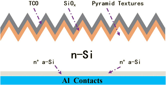
FIGURE 1. The structure diagram of TCO/SiO2/n-Si heterojunction photovoltaic devices.
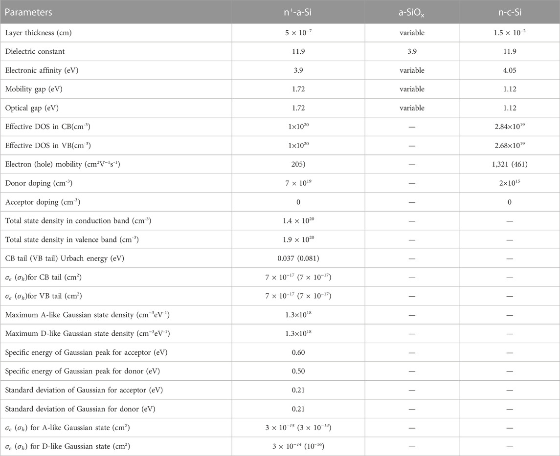
TABLE 1. Parameters set for the simulation of TCO/SiOx/n-Si with AFORS-HET.
It is a critical significance of the work function of TCO thin films for photovoltaic devices. Although the contact between TCO and the electrical layer of photovoltaic devices is assumed to be a flat band and the effect of TCO work function is ignored in many studies (Zhong et al., 2013; Varache et al., 2015), some researchers have still paid much attention to the impact of TCO work function on the performance of solar cells (Centurioni and Iencinella, 2003; Selmane et al., 2021). The influence of TCO work function on the open-circuit voltage (Voc), short-circuit current density (Jsc), fill factor (FF), and conversion efficiency (
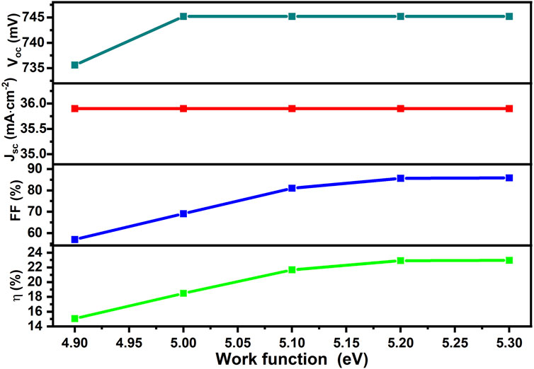
FIGURE 2. The Voc, Jsc, FF and
As shown in Figure 3, the J-V curve of the TCO/SiO2/n-Si photovoltaic device varies with the TCO work function, indicating that the J-V curve gradually shows an S-shape when the TCO work function is below 5.1 eV, while it returns to a normal rectangular shape when the TCO work function is above 5.1 eV. S-shaped J-V curves have been reported in SIS devices (Shen et al., 2010; Van Cleef et al., 1998; Kanevce and Metzger). Not only SIS heterojunction solar cells, but also HIT solar cells (Barrio et al., 2010; Chavali et al., 2014), organic solar cells (García-Sánchez et al., 2013), perovskite solar cells (Chiang et al., 2020), and polymer solar cells (Kumar et al., 2009) exhibit S-shaped J-V curves. Du Huiwei (Du et al., 2015) from our group also analyzed the S-shaped J-V curves of AZO/SiOx/n-Si and ITO/SiOx/n-Si heterojunction photovoltaic devices using equivalent circuit methods. He believed that the deformation of the J-V curve was caused by the hindrance of carrier transportation due to the thickness of insulating layer, which affected the tunneling of holes. Although the research methods and processes are different, the conclusion is consistent with the views of Cleef et al. (Van Cleef et al., 1998). Barrio (Barrio et al., 2010) and Chavali (Chavali et al., 2014) also explained the insufficient separation of carriers for the formation of S-shaped J-V curves. However, overall, there is no unified understanding of the reasons for the formation of S-shaped J-V curves in heterojunction solar cells.
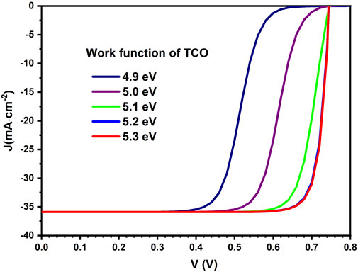
FIGURE 3. J-V curve of TCO/SiO2/n-Si solar cells with different work function of TCO.
For the TCO/SiO2/n-Si heterojunction photovoltaic device, the S-shaped J-V curve caused by the work function difference is due to the fact that the lower TCO work function causes a smaller work function difference between TCO and the silicon substrate, which results in insufficient bending of the energy band of the silicon. Therefore, there is no enough built-in electric field to quickly separate the photogenerated carriers, which results in the deformation of the J-V curve. When the TCO work function is sufficiently large, the J-V curve returns to normal. According to the simulation results in Figure 3, for the TCO/SiO2/n-Si heterojunction photovoltaic device, when the difference between the TCO work function (5.1 eV) and the c-Si work function (4.3 eV) (Gao et al., 2017) is 5.1–4.3 = 0.8 eV, the J-V curve shows a normal rectangular shape. However, when the difference between the TCO work function and the c-Si work function is less than 0.8 eV, the J-V curve rapidly evolves into an S-shape. When the difference between the TCO work function and the c-Si work function is greater than 0.8 eV, the J-V curve returns to normal. In the final analysis, when the TCO work function is not large enough, there is no built-in electric field that can quickly separate the photogenerated carriers, and the device’s ability to separate carriers is insufficient, resulting in an S-shaped J-V curve.
According to semiconductor physics, the band bending occurs on the surface of the crystalline silicon. The amount of band bending depends on the difference between the work functions of the TCO film and the crystalline silicon substrate material. Figure 4 shows the band diagram of the TCO/SiO2/n-Si heterojunction photovoltaic devices simulated with AFORS-HET. It can be seen that the band bending, i.e., the space charge region, is mainly located on the surface of the crystalline silicon, and is independent of the value of the TCO work function. The width of the space charge region is approximately 500 nm and does not change with the TCO work function. With the work function increasing, the band bending becomes more pronounced. The band bending corresponding to different work functions is approximately equal to the difference between the TCO work function and the crystalline silicon substrate work function. For example, when the TCO work function is 4.9 eV, the band bending is 4.9–4.3 = 0.6 eV. The amount of band bending determines the upper limit of the device’s open circuit voltage. Seunghun Lee et al. (Lee et al., 2013) studied the effect of TCO work function on the performance of HIT cells and found that the band bending related to the TCO work function has a significant impact on the open circuit voltage (Voc) and fill factor (FF) of TCO/a-Si:H (p)/a-Si:H (i)/c-Si (n)/a-Si:H (n)/TCO solar cells at the front interface. When the TCO work function is below 5.2 eV, carrier transport is hindered by the band bending, which is consistent with the results of other research groups (Lee et al., 2013; Rubinelli et al., 1992; Sanchez-Sinencio and Williams, 1983; Schmidt et al., 2001), fully demonstrating the importance of TCO work function for solar cell performance.

FIGURE 4. The band diagram of the TCO/SiO2/n-Si with different work function of TCO.
As introduced above, the band bending of TCO/SiO2/n-Si depends on the difference between the work functions of TCO and n-Si. Vbi is the built-in potential difference. The electric field intensity represents the gradient of the potential. Under the influence of the built-in electric field, electrons and holes are separated rapidly and transported in opposite directions, thus producing the photovoltaic effect. The built-in electric field determines the device’s ability to separate photogenerated carriers. The built-in electric field for the various TCO work function in TCO/SiO2/n-Si heterojunction photovoltaic devices were simulated and shown in Figure 5. The built-in electric field is greatly affected by the TCO work function. The electric field is relatively stable within 1 nm of the silicon surface, and gradually decreases afterwards. When the TCO work function is 5.3 eV, the maximum built-in electric field can exceed 4 × 10⁸ V cm-1. However, when the TCO work function is 4.9 eV, the built-in electric field is only 2 × 10⁶ V cm-1, which is significantly different from the electric field intensity generated when the work function is 5.3 eV. When the work function increases, the built-in electric field increases rapidly. This can also help to understand the simulation results in section 6.2.2, where the photovoltaic parameters of the device are improved as the work function increases. This is because higher work functions can excite larger electric fields, thereby enhancing the ability of TCO/SiO2/n-Si heterojunction photovoltaic devices to separate photogenerated carriers.
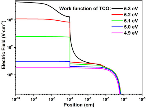
FIGURE 5. The built-in electric field of the TCO/SiO2/n-Si with different work function of TCO.
In TCO/SiO2/n-Si heterojunction photovoltaic devices, the Fermi levels of TCO and crystalline silicon are different, which causes the flow of electrons and holes and forms a built-in electric field. The electrons in the space charge region produce additional potential energy due to the built-in electric field, causing the band to bend. When the difference in work function between TCO and n-type silicon reaches a certain level, the band bending causes the Fermi level of a thin layer on the surface of the silicon to be lower than the intrinsic Fermi level or even close to the valence band maximum. At this point, a p-type thin layer is formed on the surface of the n-type silicon (as shown in Figure 6), which is called an inversion layer. The thickness of the inversion layer in TCO/SiO2/n-Si heterojunction photovoltaic devices changes with the TCO work function as shown in Table 2. As the work function increases, the thickness of the inversion layer gradually increases, but the magnitude of the increase becomes smaller and smaller. When the TCO work function is 5.3 eV, the thickness of the inversion layer reaches 265 nm. In fact, the p-type inversion layer induced by the work function difference and the n-type silicon substrate form a homogeneous p-n junction, which is the internal cause of the device photovoltaic effect. A lot of research has been done on the inversion layer in crystalline silicon, especially in MOS structures (Skocpol et al., 1986; Fischetti and Laux, 1993; Takagi et al., 2002; Ando, 2007; Ghannam et al., 2015; Yu et al., 2015; Gao et al., 2017). We believe that in the SIS structure, the inversion layer should act as the emitter. This is consistent with the view of Moustafa Ghannam (Ghannam et al., 2015) that the inversion layer acts as the emitter in the HIT structure.
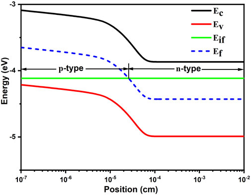
FIGURE 6. Schematic diagram of the inversion layer in TCO/SiO2/n-Si solar cells (Ec、Ev denote conduction band minimum and valance band maximum, respectively; Eif、Ef denote intrinsic Fermi level of c-Si and Fermi level of CO/SiO2/n-Si solar cells, respectively).
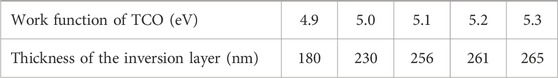
TABLE 2. Thickness of the inversion layer in TCO/SiO2/n-Si solar cells with different work function of TCO.
The thickness of the SiO2 layer determines the width of the barrier in the transport of carriers in the TCO/SiO2/n-Si heterojunction solar cell. R. Varache (Varache et al., 2015) pointed out in his study of carrier transport in solar cells that the tunneling factor decreases sharply with the increase of the thickness of the insulating layer. Therefore, studying the impact of the SiO2 layer on the performance of TCO/SiO2/n-Si heterojunction solar cells is very vital.
As shown in Table 3, the open-circuit voltage (Voc) and the short-circuit current (Jsc) of the TCO/SiO2/n-Si heterojunction photovoltaic device hardly fluctuate with the variation of SiO2 width, while the fill factor (FF) and conversion efficiency (η) rapidly decrease with the increase of SiO2 width. When the thickness of SiO2 increases from 1.8 nm to 2.3 nm, although the thickness change is only 0.5 nm, the fill factor decreases from 85.9% to 74.5%, and the conversion efficiency also drops from 22.9% to 19.9%. At the same time, as shown in Figure 7, it can be seen that with the increase of the SiO2 insulating layer thickness, the J-V curve of the TCO/SiO2/n-Si heterojunction photovoltaic device gradually exhibits an S-shape. Obviously, this is due to the increase in thickness, which reduces the tunneling probability and hinders the transport of charge carriers, thereby affecting the device performance. This is consistent with the research results of Huiwei Du (Du et al., 2015) in our research group.
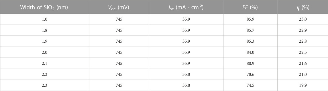
TABLE 3. The performance of TCO/SiO2/n-Si with different thickness of SiO2.
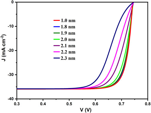
FIGURE 7. J-V curves of TCO/SiO2/n-Si solar cells with different thickness of SiO2.
Energy band offset has two main effects on the heterojunction solar cell. Firstly, the presence of a barrier can reduce recombination at the interface. Secondly, it may affect the transport of carriers and cause a decrease in the fill factor if the barrier is too high or too wide. The effect of the energy band offset at the SiOx/n-Si interface on the performance of the TCO/SiOx/n-Si heterojunction solar cell was simulated. The results show that the short-circuit current is not basically affected by the energy band offset and remains at 35.9 mA cm-2. The open-circuit voltage varies with the energy band offset, as shown in Figure 8A. When the electron barrier exceeds 0.4 eV, the open-circuit voltage reaches 745 mV and is no longer affected by the increase of the electron barrier. However, the variation of the hole barrier has almost no effect on the open-circuit voltage. As shown in Figure 8B, when the electron barrier exceeds 0.4 eV, the conversion efficiency reaches 22.9% and is no longer affected by the increase in the electron barrier. The conversion efficiency decreases slightly when the hole barrier exceeds 4 eV. Figure 8C shows the effect of the energy band offset on
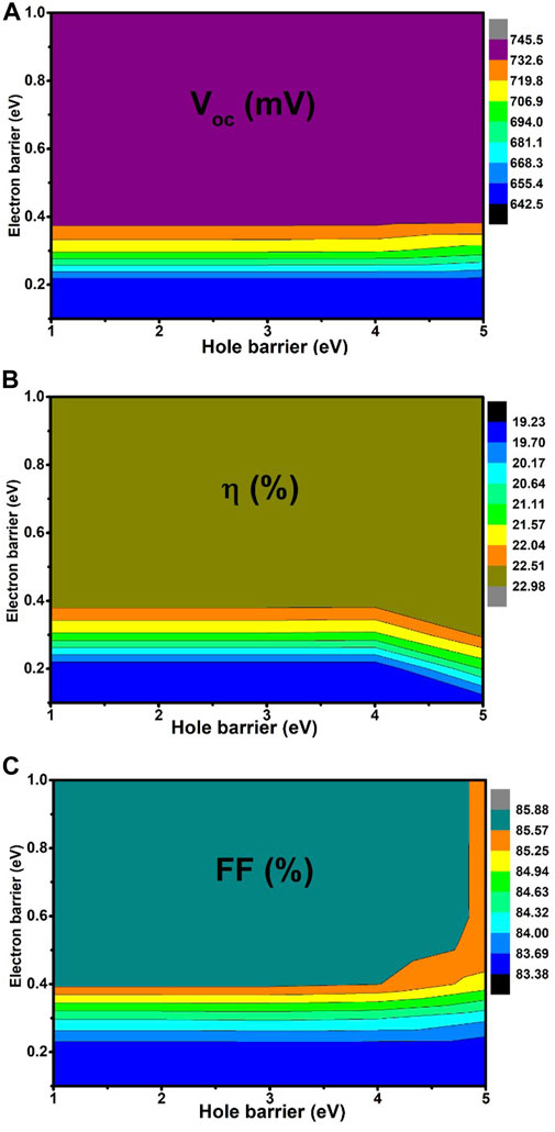
FIGURE 8. (A) Voc, (B)
An S-shaped J-V curve gradually appears when the work function difference between TCO and c-Si substrate is less than 0.8 eV. The small work function difference between TCO and c-Si materials leads to insufficient built-in electric field, making it difficult to separate the photogenerated carriers timely. In addition, we also find the J-V curve gradually shows an S-shape when the SiO2 layer thickness exceeds 2 nm. The carries have to tunnel through the high barrier of SiO2 layer, decreasing tunneling probability. Those above mentioned indicate that the formation of S-shaped J-V curves in photovoltaic devices is not unique.
Figure 9 shows S-shaped J-V curves caused by different reasons, and the reasons cannot be distinguished from the figure alone. Through summary analysis, it can be found that there are two reasons for the formation of S-shaped J-V curves in photovoltaic devices. One is that the built-in electric field is too small, resulting in insufficient ability of the device to separate photogenerated carriers, such as in TCO/SiOx/n-Si devices where the work function difference between TCO and n-Si is not large enough. The other reason is that carrier transport is hindered, such as in TCO/SiO2/n-Si devices where the SiO2 layer is too thick, or in a-Si/c-Si structures where the band offset is too large.
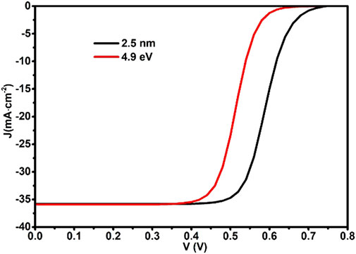
FIGURE 9. Comparison of J-V curves caused by different origins.
In order to improve the conversion efficiency of solar cells, researchers have conducted extensive exploration for a long time. Surface texturing on crystalline silicon to reduce optical losses is a common method. Texturing is a selective etching of certain planes in the crystal lattice of the silicon surface to expose pyramid-like structures, which can increase the probability of light absorption by allowing incident light to enter the cell multiple times. Because higher surface recombination rate reduces the open-circuit voltage of the cell and limits the fill factor, passivation is also an important step in improving the conversion efficiency of solar cells. Field effect passivation is the deposition of a heavily doped passivation layer on the surface of crystalline silicon, which causes the energy band on the surface to bend and form an internal electric field, suppressing charge recombination. It is used to reduce the back surface recombination rate in n/n+ or p/p+ junctions. And we will simulate the effects of surface texturing and back surface field (BSF) passivation to optimize the output parameters of TCO/SiO2/n-Si heterojunction solar cells. As shown in Table 4, the efficiency of TCO/SiO2/n-Si heterojunction solar cells are only 15.4%. Surface texturing on crystalline silicon improves both short-circuit current and open-circuit voltage, but not by much. Deposition of the back field passivation layer has a significant effect on the performance of the device, especially the open-circuit voltage, which is greatly improved; Meanwhile, the fill factor and conversion efficiency also have significant improvement. When the device has both surface texturing and back field passivation, the open-circuit voltage can reach 745 mV, with the fill factor of 85.7% and conversion efficiency of 22.9%, respectively.
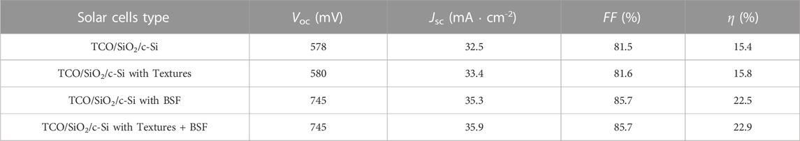
TABLE 4. Comparison of solar cell performance for TCO/SiO2/c-Si with texture and BSF.
In summary, we investigates the impact of TCO work function on the performance of TCO/SiO2/n-Si SIS solar cells by AFORS-HET simulation and proposes two mechanisms for the observed S-shape J-V curve with low FF. Optimized simulation of the non-standard SiOx insulation layer in TCO/SiOx/n-Si heterojunction solar cells is also conducted. The results show that the work function of TCO greatly affects the open-circuit voltage (Voc), fill factor (FF), and conversion efficiency of the device, while the short-circuit current (Jsc) remains largely unchanged. A higher TCO work function (5.2 eV) leads to improved Voc (745 mV), FF (85.7%), and conversion efficiency (22.9%), attributed to the increased built-in electric field and reduced carrier recombination. Additionally, the interfacial band step in TCO/SiOx/n-Si heterojunction devices effectively inhibits electron diffusion and suppresses interface recombination, resulting in excellent device performance. The research findings on TCO provide a deeper theoretical guidance for the industrial heterojunction with intrinsic thin film (HIT) solar cells. Meanwhile, the SiOx layer of SIS solar cell has the passivation and tunneling effect and plays the same role with the SiOx layer of the tunneling oxide passivation contacts (TOPCon) solar cell with mass production, deepening our understanding of TOPCon solar cells. This study provides valuable insights for enhancing the performance of industrial Si-based solar cells.
The original contributions presented in the study are included in the article/Supplementary material, further inquiries can be directed to the corresponding author.
XS: Investigation, Methodology, Writing–original draft, Writing–review and editing. CY: Writing–original draft. ZH: Writing–review and editing.
The author(s) declare financial support was received for the research, authorship, and/or publication of this article. This work was supported by the Natural Science Foundation of Jiangsu Province (BK20221395), the “Qinglan” Project of Jiangsu Education Department, the Natural Science Foundation of China (61774069), the Major projects of the Natural Science Foundation of Universities in Jiangsu Province (20KJA430013), the Lianyungang “Haiyan” Plan (2020-QD-010).
The authors declare that the research was conducted in the absence of any commercial or financial relationships that could be construed as a potential conflict of interest.
All claims expressed in this article are solely those of the authors and do not necessarily represent those of their affiliated organizations, or those of the publisher, the editors and the reviewers. Any product that may be evaluated in this article, or claim that may be made by its manufacturer, is not guaranteed or endorsed by the publisher.
Allouhi, A., Rehman, S., Buker, M. S., and Said, Z. (2022). Up-to-date literature review on Solar PV systems: technology progress, market status and R&D. J. Clean. Prod. 362, 132339. doi:10.1016/j.jclepro.2022.132339
Ando, T. (2007). Screening effect and quantum transport in a silicon inversion layer in strong magnetic fields. Magn. Fields 43 (5), 1616–1626. doi:10.1143/jpsj.43.1616
Ashok, S., Sharma, P. P., and Fonash, S. (1980). Spray-deposited ITO—silicon SIS heterojunction solar cells. IEEE Trans. Electron Devices 27 (4), 725–730. doi:10.1109/t-ed.1980.19928
Barrio, R., Gandía, J. J., Cárabe, J., González, N., Torres, I., Mu?Oz, D., Voz, C. J. S. E. M., and Cells, S. (2010). Surface recombination analysis in silicon-heterojunction solar cells. Sol. Energy Mater. Sol. Cells 94 (2), 282–286. doi:10.1016/j.solmat.2009.09.017
Bivour, M., Schröer, S., and Procedia, M. H. J. E. (2013). Numerical analysis of electrical TCO/a-Si: H (p) contact properties for silicon heterojunction solar cells. Energy Procedia 38, 658–669. doi:10.1016/j.egypro.2013.07.330
Bo, H., Quan, M. Z., Jing, X., Lei, Z., Sheng, Z. N., Feng, L., et al. (2009). Microstructures, Realization and characterization of an ITO/AZO/SiO2/p-Si SIS heterojunction. Superlattices Microstruct. 46 (4), 664–671.
Centurioni, E., and Iencinella, D. (2003). Role of front contact work function on amorphous silicon/crystalline silicon heterojunction solar cell performance. IEEE Electron Device Lett. 24 (3), 177–179. doi:10.1109/led.2003.811405
Chavali, R., Wilcox, J. R., Ray, B., Gray, J. L., Alam, M., et al. (2014). Correlated nonideal effects of dark and light I–V characteristics in a-Si/c-Si heterojunction solar cells. IEEE J. Photovoltaics 4, 763–771. doi:10.1109/jphotov.2014.2307171
Chen, S., Gao, M., and Fang, X., (2015). Modifications and multiple roles of graphene film in SIS structural solar cells. Sol. Energy 122, 658–666. doi:10.1016/j.solener.2015.09.039
Cheng, H., Huang, Z., Zhang, L., Liu, Y., Song, X., Tong, R., et al. (2022). 21.16%-efficiency p-type TOPCon solar cell with ALD-Al2O3/MoOx/Ag as a hole-selective passivating contact. Sol. Energy 247, 171–176. doi:10.1016/j.solener.2022.10.019
Chen, S., Gao, M., Wan, Y., Du, H., Li, Y., et al. (2016). Questing and the application for silicon based ternary compound within ultra-thin layer of SIS intermediate region. Appl. Surf. Sci. 388, 57–63. doi:10.1016/j.apsusc.2016.03.168
Chiang, S. E., Wu, J. R., Cheng, H. M., Hsu, C. L., Shen, J. L., Yuan, C. T., et al. (2020). Origins of the s-shape characteristic in J-V curve of inverted-type perovskite solar cells. Nanotechnology 31, 115403. doi:10.1088/1361-6528/ab5a02
Du, H. W., Yang, J., Li, Y. H., Xu, F., Xu, J., and Ma, Z. (2015). Preparation of ITO/SiOx/n-Si solar cells with non-decline potential field and hole tunneling by magnetron sputtering. Appl. Phys. Lett. 106 (9), 164–172. doi:10.1063/1.4914325
Ennaoui, A., Sankapal, B. R., Skryshevsky, V., and Lux-Steiner, M. (2006). TiO2 and TiO2–SiO2 thin films and powders by one-step soft-solution method: synthesis and characterizations. Sol. Energy Mater. Sol. Cells 90 (10), 1533–1541. doi:10.1016/j.solmat.2005.10.019
Fadakar Masouleh, F., Das, N., and Rozati, S. (2016). Nano-Structured gratings for improved light absorption efficiency in solar cells. Energies 9 (9), 756. doi:10.3390/en9090756
Fischetti, M. V., and Laux, S. E. (1993). Monte Carlo study of electron transport in silicon inversion layers. Phys. Rev. B Condens Matter 48 (4), 2244–2274. doi:10.1103/physrevb.48.2244
Gao, M., Wan, Y., Li, Y., Han, B., Song, W., Xu, F., et al. (2017). Effective passivation and tunneling hybrid a-SiOx(in) layer in ITO/n-Si heterojunction photovoltaic device. ACS Appl. Mater Interfaces 9 (20), 17565–17575. doi:10.1021/acsami.7b01447
Gao, M., Chen, D., Han, B., Song, W., Zhou, M., Song, X., et al. (2018). Bifunctional hybrid a-SiOx(Mo) layer for hole-selective and interface passivation of highly efficient MoOx/a-SiOx(Mo)/n-Si heterojunction photovoltaic device. Acs Appl. Mater. Interfaces 10 (32), 27454–27464. doi:10.1021/acsami.8b07001
García-Sánchez, F. J., Lugo-Muñoz, D., Muci, J., and Ortiz-Conde, A. (2013). Lumped parameter modeling of organic solar cells' S-shaped I–V characteristics. IEEE J. Photovolt. 3 (1), 330–335. doi:10.1109/jphotov.2012.2219503
Ghannam, M., Shehadah, G., Abdulraheem, Y., and Poortmans, J. (2015). On the possible role of the interfacial inversion layer in the improvement of the performance of hydrogenated amorphous silicon/crystalline silicon heterojunction solar cells [HIT]. Sol. Energy Mater. Sol. Cells 132, 320–328. doi:10.1016/j.solmat.2014.09.008
Simashkevich, A., Serban, D., Bruc, L., Curmei, N., Hinrichs, V., and Rusu, M. (2016). Indium tin oxide thin-films prepared by vapor phase pyrolysis for efficient silicon based solar cells. Thin Solid Films 610, 35–41. doi:10.1016/j.tsf.2016.04.047
Huang, Z., Zhong, S., Hua, X., Lin, X., Kong, X., Dai, N., et al. (2017). An effective way to simultaneous realization of excellent optical and electrical performance in large-scale si nano/microstructures. Prog. Photovoltaics Res. Appl. 23, 964–972. doi:10.1002/pip.2506
Huang, Z. G., Gao, K., Wang, X. G., Xu, C., Song, X. M., Shi, L. X., et al. (2019). Large-area MACE Si nano-inverted-pyramids for PERC solar cell application. Sol. Energy 188 (AUG), 300–304. doi:10.1016/j.solener.2019.06.015
Kanevce, A., and Metzger, W. (2009). The role of amorphous silicon and tunneling in heterojunction with intrinsic thin layer (HIT) solar cells. J. Appl. Phys. 105 (9), 932–711. doi:10.1063/1.3106642
Kobayashi, H., Ishida, T., Nakato, Y., and Tsubomura, H. (1991). Mechanism of carrier transport in highly efficient solar cells having indium tin oxide/Si junctions. J. Appl. Phys. 69 (3), 1736–1743. doi:10.1063/1.347220
Korte, L. (2012). Electronic properties of ultrathin a-Si:H layers and the a-Si:H/c-Si interface. Springer Berlin Germany.
Kumar, A., Sista, S., and Yang, Y. (2009). Dipole induced anomalous S-shape I-V curves in polymer solar cells. J. Appl. Phys. 105 (9), 497. doi:10.1063/1.3117513
Lee, S., Tark, S. J., Kim, C. S., Jeong, D. Y., Lee, J. C., Kim, W. M., et al. (2013). Influence of front contact work function on silicon heterojunction solar cell performance. Curr. Appl. Phys. 13 (5), 836–840. doi:10.1016/j.cap.2012.12.013
Liu, Y., Sang, B., Hossain, M. A., Gao, K., Cheng, H., Song, X., et al. (2021). A novel passivating electron contact for high-performance silicon solar cells by ALD Al-doped TiO2. Sol. Energy 228, 531–539. doi:10.1016/j.solener.2021.09.083
Lupangu, C., and Bansal, R. C. (2017). A review of technical issues on the development of solar photovoltaic systems. Renew. Sustain. Energy Rev. 73, 950–965. doi:10.1016/j.rser.2017.02.003
Malik, O., Grimalsky, V., Torres-J, A., and Hidalga-W, J. (2004). “Room temperature electroluminescence from metal oxide-silicon surface-barrier diode,” in International Conference on Microelectronics, Tunis, Tunisia, December 2004.
Malik, O., Hidalga-W, F. J. D. L., Zuniga-I, C., Torres-J, A., and Ruiz-T, G. J. I. (2008). “Experimental and theoretical analysis of the conversion efficiency of ITO- nSi solar cells fabricated by a low-cost spray deposition technique,” in 2008 33rd IEEE Photovoltaic Specialists Conference, San Diego, CA, USA, May 2008.
Maruska, H. P., Ghosh, A. K., Eustace, D. J., and Feng, T. (1983). Interfacial stability of SnO2/n-Si and In2O3:Sn/n-Si heterojunction solar cells. J. Appl. Phys. 54 (5), 2489–2494. doi:10.1063/1.332366
Pandey, A. K., Tyagi, V. V., Selvaraj, J. A. L., Rahim, N. A., and Tyagi, S. K. (2016). Recent advances in solar photovoltaic systems for emerging trends and advanced applications. Renew. Sustain. Energy Rev. 53, 859–884. doi:10.1016/j.rser.2015.09.043
Rubinelli, F. A., Arch, J. K., and Fonash, S. (1992). Effect of contact barrier heights on a-Si:H p-i-n detector and solar-cell performance. J. Appl. Phys. 72 (4), 1621–1630. doi:10.1063/1.351679
Sanchez-Sinencio, F., and Williams, R. (1983). Barrier at the interface between amorphous silicon and transparent conducting oxides and its influence on solar cell performance. J. Appl. Phys. 54 (5), 2757–2760. doi:10.1063/1.332303
Schmidt, M., Froitzheim, A., Stangl, R., Elstner, L., and Fuhs, W. (2001). “Photocurrent analysis in TCO a Si H c Si solarcell structures,” in 17th european photovoltaic solar energy conference, Munich, Germany, October 2001.
Selmane, N., Cheknane, A., Bellakhdar, A., and Khemloul, F. (2021). “A high efficiency (∼25.62%): influence of thickness and work function of transparent conducting oxide of the performance of heterojunction solar cells,” in Séminaire International sur l’Industrie et la Technologie, Webinaire par internet à travers Google Meet, Tlemcen, Algeria, March 2021.
Shelat, N., Das, N., Khan, M. M. K., and Islam, S. (2020). “Nano-structured photovoltaic cell design for high conversion efficiency by optimizing various parameters,” in 2019 29th Australasian Universities Power Engineering Conference (AUPEC), Nadi, Fiji, November 2020.
Shen, L., Du, H. W., Ding, H., Tang, J., and Ma, Z. Q. (2010). Region-dependent behavior of I–V characteristics in n-ZnO:Al/p-Si contacts. Mater. Sci. Semicond. Process. 13, 339–343. doi:10.1016/j.mssp.2011.02.021
Skocpol, W. J., Mankiewich, P. M., Howard, R. E., Jackel, L. D., and Stone, A. D. (1986). Universal conductance fluctuations in silicon inversion-layer nanostructures. Phys. Rev. Lett. 56 (26), 2865–2868. doi:10.1103/physrevlett.56.2865
Song, X. M., Gao, M., Huang, Z. G., Han, B. C., Ma, Z. Q. J. S. E., Lei, Q., et al. (2018). Interface properties of ITO/n-Si heterojunction solar cell: quantum tunneling, passivation and hole-selective contacts. Sol. Energy 173, 456–461. doi:10.1016/j.solener.2018.07.083
Takagi, S. I., Toriumi, A., Iwase, M., and Tango, H. (2002). On the universality of inversion layer mobility in Si MOSFET's: Part I-effects of substrate impurity concentration. IEEE Trans. Electron Devices 41 (12), 2357–2362. doi:10.1109/16.337449
Van Cleef, M. W. M., Schropp, R. E. I., and Rubinelli, F. (1998). Significance of tunneling in p+ amorphous silicon carbide n crystalline silicon heterojunction solar cells. Appl. Phys. Lett. 73 (18), 2609–2611. doi:10.1063/1.122521
Varache, R., Leendertz, C., Gueunier-Farret, M. E., Haschke, J., Muñoz, D., and Korte, L. (2015). Investigation of selective junctions using a newly developed tunnel current model for solar cell applications. Sol. Energy Mater. Sol. Cells 141, 14–23. doi:10.1016/j.solmat.2015.05.014
Wenas, W. W., and Riyadi, S. (2006). Carrier transport in high-efficiency ZnO/SiO2/Si solar cells. Sol. Energy Mater. Sol. Cells 90 (18-19), 3261–3267. doi:10.1016/j.solmat.2006.06.026
Yu, X., Shen, X., Mu, X., Zhang, J., Sun, B., Zeng, L., et al. (2015). High efficiency organic/silicon-nanowire hybrid solar cells: significance of strong inversion layer. Sci. Rep. 5, 17371. doi:10.1038/srep17371
Keywords: SIS solar cells, heterojunction, TCO/SiOx/n-Si, tunneling, AFORS-HET
Citation: Song XM, Ye CY and Huang ZG (2023) Optimization of SIS solar cells with ultra-thin silicon oxide layer. Front. Energy Res. 11:1283196. doi: 10.3389/fenrg.2023.1283196
Received: 25 August 2023; Accepted: 02 November 2023;
Published: 14 November 2023.
Edited by:
Malek Masmoudi, Université Jean Monnet, FranceReviewed by:
Khaled Obaideen, University of Sharjah, United Arab EmiratesCopyright © 2023 Song, Ye and Huang. This is an open-access article distributed under the terms of the Creative Commons Attribution License (CC BY). The use, distribution or reproduction in other forums is permitted, provided the original author(s) and the copyright owner(s) are credited and that the original publication in this journal is cited, in accordance with accepted academic practice. No use, distribution or reproduction is permitted which does not comply with these terms.
*Correspondence: X. M. Song, eG1zb25nQGpvdS5lZHUuY24=
Disclaimer: All claims expressed in this article are solely those of the authors and do not necessarily represent those of their affiliated organizations, or those of the publisher, the editors and the reviewers. Any product that may be evaluated in this article or claim that may be made by its manufacturer is not guaranteed or endorsed by the publisher.
Research integrity at Frontiers
Learn more about the work of our research integrity team to safeguard the quality of each article we publish.