- 1School of Automation, Northwestern Polytechnical University, Xi’an, China
- 2College of Science for Women, University of Baghdad, Baghdad, Iraq
- 3Department of Renewable Energy, National Advanced School of Engineering of Maroua, University of Maroua, Maroua, Far North Region, Cameroon
- 4Department of Electronics Engineering, University of Engineering and Technology, Peshawar, Peshawar, Khyber Pakhtunkhwa, Pakistan
This paper introduces a DC-DC converter that employs a modified triple boosting architecture (MTB), interleaved with modified switched inductor capacitors (MSIC), to achieve ultra-high voltage gain in photovoltaic applications. The converter design also includes a modified switched inductor with a modified voltage multiplier mode (MVM), which interleaves with the main switch and effectively doubles the voltage transfer gain. Furthermore, a modified triple boosting mode technique, utilizing interleaved components and an auxiliary switch, is integrated into the converter design. The main switch and auxiliary switch, combined with modified voltage multiplyer, contribute to achieving high voltage gain. The proposed converter offers numerous advantages. It exhibits remarkable efficiency while ensuring low voltage stress across diodes and MOSFETs. Moreover, by utilizing low inductance and capacitance values at high switching frequencies, the converter’s overall performance is enhanced. To validate and substantiate the simulation and laboratory results, the converter has undergone PCB design and experimental testing. Specifically, this converter is designed to boost input voltage levels ranging from 30 V to 40 V to a variable output voltage between 200 V and 400 V, with a power output of 360 W and an efficiency rating of 96.5%.
1 Introduction
A DC-DC converter is a vital electronic device used to convert one level of DC voltage to another, ensuring efficient power management in various applications (Babaei et al., 2018a; Abbasi and Lam, 2019; Azizkandi et al., 2019; Mirzaee and Moghani, 2019; Elsayad et al., 2020; Folmer and Stala, 2021; Hasanpour et al., 2021; Rahimi et al., 2021; Abbasian et al., 2022; Mohammadi et al., 2022; Rahimi et al., 2022; Farahani et al., 2023; Hasanpour et al., 2023; Rajesh and Prabaharan, 2023). This versatile device accepts a DC input voltage and delivers a regulated output voltage of a different level, allowing compatibility between power sources and loads. DC-DC converters are extensively employed in diverse fields such as telecommunications, automotive, renewable energy, and portable electronics (Abbasi and Lam, 2019; Rahimi et al., 2021; Rajesh and Prabaharan, 2023). By utilizing switching techniques and control circuitry, these converters efficiently step up or step down the voltage levels while minimizing power loss (Babaei et al., 2018b; Fardahar and Sabahi, 2019; Premkumar et al., 2019; Allehyani, 2021; Zaid et al., 2021a; Zaid et al., 2021b; Pashaie et al., 2023). Their compact size, high efficiency, and reliable performance make them indispensable for optimizing power utilization and meeting the voltage requirements of modern electronic systems (Mirzaee and Moghani, 2019; Farahani et al., 2023; Hasanpour et al., 2023). Many researchers have put forth various technologies for DC-DC converters, which can be broadly divided into two types: isolated converters that use coupled inductors or transformers, and non-isolated converters that use coupled inductors without transformers. Several modified DC-DC converters have been proposed to address specific requirements and improve performance. In (Abbasian et al., 2022) introduces a modified DC-DC boost converter that utilizes extendable capacitor voltage multiplier cells (VMCs) and coupled inductors (CIs) with a clamp circuit. This design aims to reduce leakage inductances and achieve a higher voltage gain. Similarly, in reference (Azizkandi et al., 2019), a modified DC-DC converter based on coupled-inductor with three windings is presented, incorporating a passive clamp circuit to recycle the energy of leakage inductance and a voltage multiplier cell to achieve a very high-voltage conversion ratio. For renewable energy applications, in (Hasanpour et al., 2021; Rahimi et al., 2021; Hasanpour et al., 2023; Rajesh and Prabaharan, 2023) proposes a modified interleaved high step-up DC-DC converter that employs coupled inductors (CIs) and integrates switched-capacitor (SC) (VMCs) with a passive diode-capacitor clamp built-in transformer (BIT). Furthermore, in (Hasanpour et al., 2021) suggests a modified configuration of a quasi-resonant high-gain single-ended primary inductor converter (SEPIC)-based DC-DC converter, incorporating a coupled inductor (CI), (VM), and a regenerative passive lossless clamp circuit to enhance the voltage conversion ratio. In the context of photovoltaic (PV) applications, in (Rahimi et al., 2022) proposes a modified DC-DC converter utilizing a dual-switch structure with a three-winding coupled inductor (3WCI) and (SC), achieving a high-voltage gain suitable for PV systems. Additionally, in (Li et al., 2023) presents a modified quadratic boost converter that integrates a (CI) with a clamp circuit and a (VM). In (Das and Agarwal, 2016; Ardi and Ajami, 2018; Shaw and Sahoo, 2018; Sundaramoorthy, 2019; Kumar et al., 2020; Mansour and Zaky, 2023) focus on modifying the SEPIC converter by employing a (CI), with two (VM), and incorporating a passive clamp circuit to enhance its performance.
These converters have achieved significant advancements in terms of generating high voltage output. However, they suffer from various limitations that hinder their overall performance. These drawbacks include the excessive use of both passive and active components, a large number of diodes, increased resistance in inductors and capacitors, resulting in reduced efficiency. Additionally, attempting to increase the voltage gain by increasing the turn ratio of coupled inductors leads to higher internal resistance, further compromising system efficiency. Another challenge arises from the low switching frequency used in these converters, which necessitates the use of bulky inductors and capacitors. Moreover, the voltage gain is negatively affected by the on-resistance (Ron) of the power MOSFET, leading to decreased system efficiency. Furthermore, the presence of coupled inductor converters results in high spike voltages during the power switch’s off state due to the inductance of the parasitic capacitance associated with the power MOSFET switch. To address this issue, a clamped circuit can be implemented with the power switch. However, this solution introduces higher costs and reduced efficiency due to parasitic effects.
Several topologies have been proposed that incorporate the interleaving of conventional and modified converters. In (Babaei et al., 2018a), a nonisolated high DC-DC converter is presented, which utilizes Active-Passive Inductor Cells (APICs) operating based on parallel charging and series discharging of the inductors. In (Rajesh and Prabaharan, 2023) introduces a high gain nonisolated DC-DC converter achieved by combining the modified quadratic boost converter (MQDBC) with the unique (VMC). Similarly, in reference (Farahani et al., 2023), a modified non-isolated DC-DC converter based on a switched-inductor/switched-capacitor network is proposed, taking advantage of both active and passive switched inductor cells. In (Elsayad et al., 2020) proposes a modified SEPIC-based step-up DC-DC converter that integrates a discontinuous-current quasi-Z-source (qZS) and (SC) networks. In (Shaw and Sahoo, 2018; Sundaramoorthy, 2019; Kumar et al., 2020) describe a novel non-isolated high gain DC-DC (NHGDC) converter utilizing a switched inductor-capacitor network. In reference (Kumar et al., 2020), a modified conventional quadratic boost converter (QBC) is presented, incorporating a switched capacitor-inductor network (SCLN) to achieve voltage gain. For renewable energy applications, in (Babaei et al., 2018b; Zaid et al., 2021b; Khan et al., 2021; Dhananjaya et al., 2023; Mansour and Zaky, 2023) proposes a high gain DC-DC boost converter that utilizes (SL) and (SC), along with a (VMC). Lastly, reference (Gu et al., 2018) presents a modified DC-DC converter with an active switched LC-network, which introduces an active switched capacitor (ASC) network based on a transformerless DC-DC converter with an active switched inductor (ASL) network. Notwithstanding their impressive ability to achieve significant voltage gain ratios, these converters have certain limitations. The high gain ratio requires an excessively high duty ratio, unfortunately leading to increased switching and conduction losses, reduced efficiency, and compromised power density. Furthermore, the elevated duty ratio puts significant voltage stress on crucial components such as power switches, diodes, and inductors. Consequently, these components experience substantial strain, potentially impacting their reliability and lifespan. Additionally, these converters often incorporate multiple inductors and operate at a low switching frequency. While this design approach aims to improve performance and efficiency, it inadvertently introduces higher levels of parasitic resistance. Consequently, the converters suffer a decline in overall performance and efficiency, thereby limiting their effectiveness in practical applications.
On the other hand, some scientists have investigated different methods and created non-isolation DC-DC converters that can achieve significant voltage amplification without using transformers or linked inductors. These converters rely on the (SL) and (SC) technique. In (Folmer and Stala, 2021) introduces a modified DC-DC converter that utilizes resonant (SC) circuits with five MOSFET switches. In (Veerachary and Sen, 2022) proposes a topological evolution of a (SC) based boost converter, where a dual-switch configuration with a common ground feature is employed. In (Mansour et al., 2022), a non-isolated high-voltage gain DC-DC converter is presented by merging a dual boost converter with a (SL) structure. In (Allehyani, 2021) proposes a new transformerless DC-DC converter for renewable energy systems by incorporating a (SL/SC) and a (VM) stage into the traditional boost converter. Furthermore, in (Zaid et al., 2021a) describes an improved high-gain DC-DC boost converter that utilizes two (VMCs) consisting of (SC) and (SL) to enhance the voltage gain. Finally, in (Fardahar and Sabahi, 2019; Allehyani, 2021; Zaid et al., 2021a; Mansour et al., 2022; Singh et al., 2022; Pashaie et al., 2023) discuss a proposed basic bidirectional converter with five switches based on the (SC-SI) configuration. However, these converters have the advantage of achieving high voltage gain ratios. Nonetheless, they also suffer from certain limitations that impact their performance and restrict their practicality. These limitations encompass the requirement for high duty ratios, leading to increased losses and decreased efficiency. Moreover, these converters can adversely affect component durability and introduce elevated parasitic resistance due to the use of multiple inductors and low switching frequency. Despite their capability to achieve substantial voltage gain, these converters are hindered by a large number of components that detrimentally influence both system efficiency and performance. Furthermore, the power switch is subjected to high voltage and current stress, while the gate control circuit is intricate and demands a considerable amount of space for implementation.
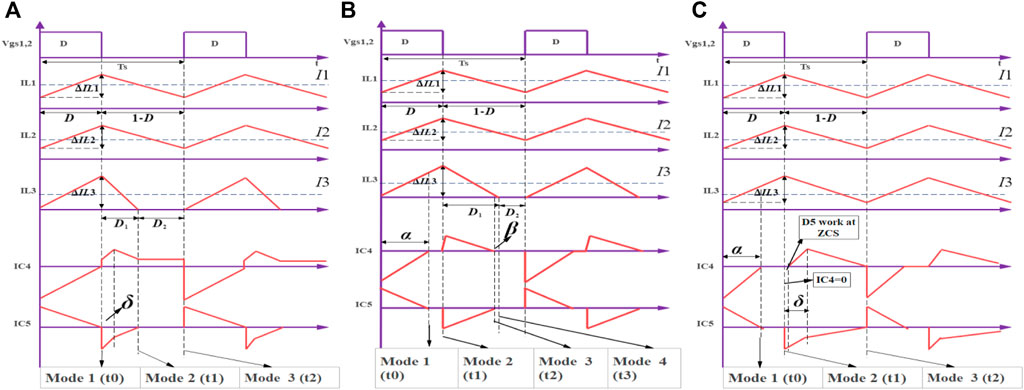
In this paper, a DC-DC converter that employs a modified triple boosting architecture interleaved with modified switched inductor capacitors is presented to achieve ultra-high voltage gain in photovoltaic applications. The converter design also includes a modified switched inductor with a modified voltage multiplier mode, which interleaves with the main switch and effectively doubles the voltage transfer gain. Furthermore, a modified triple boosting mode technique, utilizing interleaved components and an auxiliary switch, is integrated into the converter design. The main switch and auxiliary switch, combined with modified switched capacitors, contribute to achieving high voltage gain. Additionally, the diode of (MTB) D5 operates at ZCS (Zero Current Switching) when the converter operates in DCM (Discontinuous Conduction Mode) and the capacitor charge becomes zero at (β) as shown in Figure 2B. Moreover, D5 operates at ZCS when the proposed converter operates in CCM (Continuous Conduction Mode) while supplying high current. Furthermore, the diode of MTB D6 operates at ZCS when the capacitor charge becomes zero at (α) as shown in Figures 2B, 4B. Moreover, the diode of (MVM) D3 operates at ZCS at time (δ) as shown in Figures 2B, 4B. Additionally, dual PI controllers for current and voltage are designed to verify a fixed output voltage.
2 Operation principle of the Proposed DC DC converter and structure
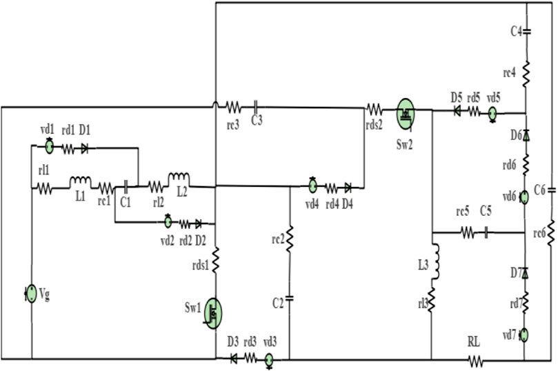
A DC-DC converter has been introduced to achieve ultra-high voltage gain and high efficiency. Its purpose is to boost a low input voltage, ranging from 30 V to 40 V, to a variable output voltage of 200 V–400 V while accommodating a 360 W load. The designed converter specifically caters to Renewable Energy Sources (RES). Figure 1A illustrates the integration of the proposed converter with PV Panels and Battery, showcasing its suitability for a low input voltage source. The schematic diagram of this new interleaved converter is presented in Figure 1B, which comprises three primary inductors, six capacitors, seven diodes, and two power MOSFET switches. This converter offers numerous notable advantages. Firstly, it eliminates the necessity for isolated coupled inductors and transformers typically required for voltage stepping. By operating at a high switching frequency, the values of inductors and capacitors can be significantly reduced, resulting in enhanced overall efficiency of the converter. Moreover, the converter’s structure is straightforward and easy to implement. The absence of pulsation in the input current at very low duty cycles enhances its reliability, particularly for photovoltaic applications. In the proposed converter, the diode (MTB) D5 exhibits (ZCS) behavior during operation in (DCM). This occurs when the capacitor charge reaches zero at (β), as depicted in Figure 2B. Additionally, when the converter operates in (CCM) and supplies high current, D5 also operates at ZCS. Similarly, the diode of (MTB) D6 achieves ZCS when the capacitor charge becomes zero at (α), as shown in both Figures 2B, 4B. Furthermore, the diode (MVM) D3 attains ZCS at time (δ), as illustrated in Figures 2B, 4B. This characteristic leads to reduced overall losses and significantly improved efficiency in the converter’s operation. In summary, the converter employs ZCS in various scenarios, providing enhanced performance and efficiency in different conduction modes and under specific conditions for the mentioned diodes. Additionally, the proposed converter guarantees low voltage stress on both the main and auxiliary switches, leading to enhanced reliability, longevity, and overall performance. This feature effectively manages voltage stress, providing a robust and durable solution for high voltage gain applications. Compared to previous DC-DC converters, the proposed design achieves a higher voltage gain while utilizing fewer inductors and capacitors. The PWM generator controlling the MOSFET switches is simple, with both devices turning on and off simultaneously, simplifying the control mechanism.

FIGURE 1. (A) Schematic diagram of the proposed converter connected with PV panels or battery. (B) Circuit diagram of the proposed DC-DC converter.
2.1 The proposed converter operation
The proposed DC-DC converter offers versatile operation in two distinct modes. The first mode, known as DCM, is employed during periods of low duty ratio and light load. The proposed converter operates in two DCM modes (DCM1 and DCM2). DCM1 appears when the proposed converter supplies a load of 360 W with a duty cycle of 33%, and DCM2 appears when the proposed converter supplies a load above 360 W with a duty ratio between 33% and 55% as shown in Figure 5A, B. In addition, this mode is particularly useful during energy-saving nighttime operations. Additionally, the DCM mode is activated when the converter operates at the minimum input voltage, making it suitable for light load applications. On the other hand, the proposed DC-DC converter also supports CCM, which comes into play when the load current is increased throughout the day. This mode allows the converter to efficiently handle higher current demands, ensuring optimal performance and stability during periods of elevated load.
2.2 The proposed converter operation at DCM1
The proposed DC-DC converter operates in DCM when the load is about 360 W the input voltage is 30 V. The current waveform of the proposed converter operating in DCM1 is shown in Figure 2A. There are three modes of operation for the proposed converter in DCM1. The operation modes are listed below.
Mode 1: [0-t0]. In this mode, both MOSFETs Sw1 and Sw2 are simultaneously activated. During this period, D1, D2, and D6 are in an “on” state, while D3, D4, D5, and D7 are in an “off” state. The inductor L1 begins to accumulate energy from the input source, while L2 also stores energy from the input source via D1. Both inductors maintain an identical current flow. The current of Capacitors C4 and C6 will be subtracted from the current through capacitor C2, which is equal to the current through C3, to discharge their energy and to charge L3 through Sw2. Furthermore, C5 undergoes charging through Sw2 from C4, C2, and C3 through D6. The proposed converter configuration for Mode 1 is illustrated in Figure 3A.
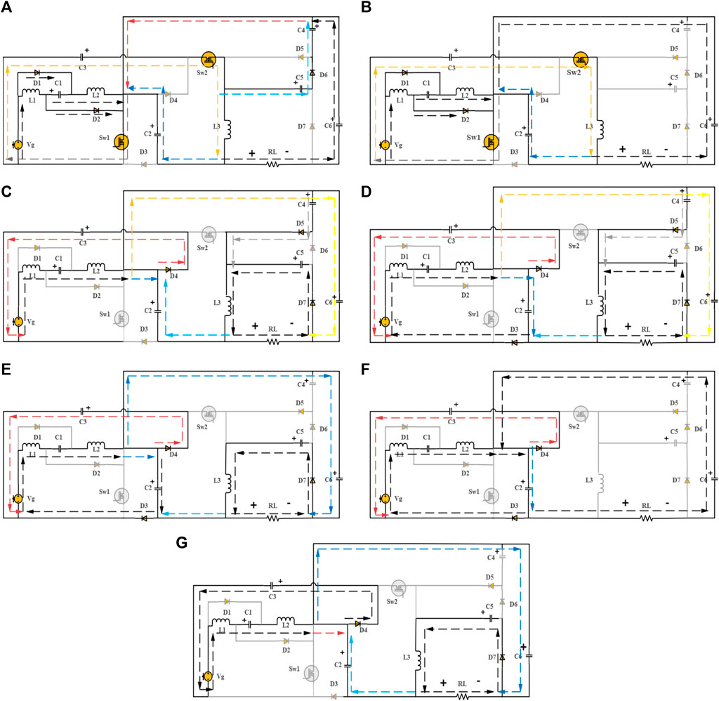
FIGURE 3. (A) Mode 1 DCM1, Mode 1 DCM2, Mode 1 CCM (B) Mode 2 DCM2, Mode 2 CCM, (C) Mode 2 DCM1, Mode 3 DCM2 (D) Mode 3 DCM2, Mode 3 CCM (E) Mode 3 DCM2 (F) Mode 3 DCM1, Mode 4 DCM2 (G) Mode 3 CCM
The voltage across inductor are shown in Eq. 1,
The voltage across capacitors are shown in Eq. 2,
Output voltage of the proposed converter can be calculated as in Eq. 3
Input current and current through power MOSFETs can be found as shown in Eqs 4, 5 respectively.
The current through diodes and capacitors can be found as shown in Eqs 6, 7 respectively.
Mode 2: [t0-t1] During this mode, both MOSFETs are turned off, and the diodes D1 and D2 are also turned off. The energy stored in inductor L1 is transferred to capacitor C1 through a series connection with L2. Additionally, L1 and L2 discharge their energy to charge capacitors C4 and C6. Meanwhile, L3 will start discharging energy through the load and through C2 for a specific time, denoted as (δ). D3 will be in the off state during this time (δ), while D4 will be in the on state, as shown in Figure 3C. During this time, D3 will operate at ZCS as shown in Figure 4B, allowing the current to pass to charge C2. After (δ), D3 will be in the on state, and the current will pass through it from C2.
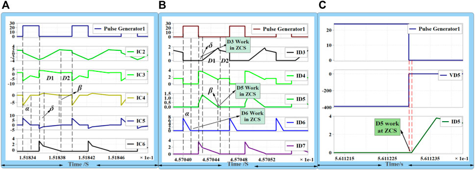
FIGURE 4. (A) Current through capacitors at DCM (B) Current through diodes at DCM (C) Voltage across D5 and current through D5 at CCM.
The voltage across inductor are shown in Eq. 8,
The current equations of this mode are shown below:
Mode 3: [t1-t2]: During this mode, both MOSFETs are turned off, and the diodes D1 and D2 are also turned off. Additionally, D5, D6, and D7 are in an off state. The energy stored in inductor L1 is transferred to capacitor C1 through a series connection with L2. D3 and D4 will remain in the on state. Meanwhile, L1 and L2 discharge their energy to charge capacitors C3 and C2 during this time. At the same time, L3 will have zero energy during this mode at time (D2), and the current through C4 and C5 will reach zero, with the same current as L3, as shown in Figures 4A, B. On the other hand, C6 will supply the load current, as illustrated in Figure 3F. The voltage equations of this mode are the same as the previous mode. The current equations of this mode are listed below:
2.3 The proposed converter operation at DCM2
The proposed DC-DC converter operates in DCM2 when the proposed converter is supplied load above 360 W. The current waveform of the proposed converter operating in DCM is shown in Figure 2B. There are four modes of operation for the proposed converter in DCM2. The operation modes are listed below:
Mode 1: [0-t0]. Same Mode 1 DCM1, Mode 2: [t0-t1]: In this mode, both MOSFETs are still in the on state after (α), and D1 and D2 are also still on. Additionally, D3 and D4 will remain in the off state. L1 and L2 continue to charge from the input source. The charge of C4 will become zero, and L3 will continue to charge from C3 after subtracting the current of C6 and C2. D6 will be in the off state after (α) at this time and will operate at ZCS during this mode as shown in Figure 4B. The current passing through C6 is equivalent to the load current. The proposed converter configuration for Mode 2 is illustrated in Figure 3B.
Mode 3: [t1-t2]: During this mode, both MOSFETs are turned off, and the diodes D1 and D2 are also off. The energy stored in inductor L1 is transferred to capacitor C1 through a series connection with L2. Additionally, L1 and L2 discharge their energy to charge capacitors C4 and C6. D5 and D7 are now in an on state and will pass current through C4 and C6, respectively. Meanwhile, L3 will start discharging energy during time (D1) through the load and through C2 for a specific time (δ), as shown in Figure 4B. D3 will be in an off state and will operate at ZCS while the current passes to charge C2 at this time (δ). D4 will be in an on state. After this time (δ), D3 will turn on, and C4 will charge until a specific time (β) as shown in Figures 2B, 4A. Following this specific time (β), D5 will change from the on state to the off state, and D5 will operate at ZCS during this time, as shown in Figure 4B. Meanwhile, C5 will continue discharging current during time (D1) through L3 to supply current to the load. After time (δ), the current through C3 and C2 will start increasing and will charge them from L1 at the same time as charging C4 and C6. The proposed converter circuit diagram of this mode as shown in Figures 3C–E.
Mode 4: [t2-t3]: same Mode 3 DCM1.
2.4 Operation of the proposed converter in CCM
As the load current increases, the converter transitions into (CCM). In CCM, both the input current and the current flowing through all inductors operate continuously. This mode allows the converter to achieve a notably higher voltage transfer ratio. Figure 2C illustrates the three operation modes in this scenario and showcases the corresponding current waveforms of the proposed converter when operating in CCM.
Mode 1: [0 to t0], Same Mode 1 DCM2,
Mode 2: [t0-t1]: Same Mode 2 DCM2.
Mode 3 [t1-t2]: During this mode, both MOSFETs are turned off, and diodes D1 and D2 are also off. The energy stored in inductor L1 is transferred to capacitor C1 through a series connection with L2. Additionally, L1 and L2 discharge their energy to charge capacitors C4 and C6. After time (δ), the current through C3 and C2 will start increasing, charging them from L1 while charging C4 and C6 simultaneously. D7 is now in an on state and will pass current through C6, while D5 is in the off state for a specific time, as shown in Figure 4C. D5 operate at ZCS for small time. Meanwhile, L3 will start discharging energy through the load and through C2 for a specific time (δ). D3 will be in an off state and will operate at ZCS while the current passes to charge C2 during this time (δ). D4 will be in an on state as shown in Figure 3G. After this time (δ), D3 will turn on, and C4 will charge until a specific time (β), as shown in Figures 2B, 4A. D5 will change from the off to the on state, and D5 will pass C4 current. Meanwhile, C5 will continue discharging current through L3 to supply current to the load. The proposed converter circuit diagram of this mode is shown in Figure 3D.
The proposed converter utilizes diodes D5 and D6, which exhibit (ZCS) behavior during operation in (DCM). In this mode, when the capacitor charge reaches zero at (β) as depicted in Figure 2B, D5 operates at ZCS. Furthermore, during (CCM) and when the converter supplies high current, D5 also operates at ZCS. Similarly, diode D6 achieves ZCS when the capacitor charge becomes zero at (α), as shown in both Figures 2B, 4B . Another diode, D3, achieves ZCS at time (δ), as illustrated in Figures 2B, 4B. The utilization of ZCS in various scenarios results in reduced overall losses and significantly improved efficiency during the converter’s operation. This enhancement applies to different conduction modes and under specific conditions for the mentioned diodes. Moreover, the converter design ensures low voltage stress on both the main and auxiliary switches, which leads to enhanced reliability, longevity, and overall performance. The effective management of voltage stress provides a robust and durable solution, especially in high voltage gain applications.
Figures 5A, B illustrate the boundary conditions governing the operation of the proposed converter in both (DCM) and (CCM). It is evident that the converter can operate in DCM when the duty ratio is below 50%, and in CCM when the load current is increased and the duty ratio goes above 55%, as indicated by Eq. 30.

FIGURE 5. The boundary condition of the proposed converter operation (A) KCrit Vs. load less factor, (B) K Vs. duty cycle.
3 Voltage transfer gain calculation
In this section, the voltage transfer gain of the proposed converter is calculated in both DCM and CCM.
3.1 Voltage transfer gain calculation at CCM
The suggested converter has the capability to function in (CCM) when handling high load currents. Consequently, the voltage gain of the proposed converter can be obtained in CCM, as depicted by the following equations:
To determine the voltage gain of the suggested converter, Eqs 1, 8 are utilized. By applying volt-second balance to L1, L2, and L3, the resulting Eqs 15, 16. Solving these Eqs 20, 21. Additionally, Eqs 17, 18 correspond to the peak current of inductors L1, L2, and L3, respectively. Finally, Eq. 19 represents the voltage across C1, which is equivalent to the input voltage.
Eq. 22 expresses the connection between the output voltage and the input voltage, defining the voltage gain equation of the proposed converter in (CCM). It is evident from Eq. 22 that the proposed converter exhibits a higher voltage gain compared to previous DC-DC converters.
3.2 Voltage transfer gain calculation at DCM
In this section, the proposed converter is operated in DCM at a low duty ratio, which is below 50%. This allows us to derive the voltage gain of the proposed converter when the system operates in DCM.
The voltage transfer gain of the proposed converter can be derived by employing volt-second balance to the inductors L1, L2, and L3, based on Eqs 1, 8. This approach leads to Eq. 23. Furthermore, by utilizing the fact that the average voltage across capacitor C1 equals the input voltage, we can solve for Eqs 24, 25. In this context, (D1) symbolizes the discharging time of inductor L3. Eq. 26 offer the average inductor current in L3.
Eq. 27 defines the average output current, while Eq. 28 establishes the correlation between the output voltage and the input voltage in DCM. It is evident from Eq. 28 that the voltage gain relies on the load resistor, duty ratio, and switching frequency (RL, D, Fs). Expressing the voltage gain of the proposed converter as a function of the load loss factor (K), Eq. 29 emerges. Determining the critical value of K (Kcrit) is achievable using Eq. 30, which leads to the derived expression given in Eq. 30. Eq. 30 serves as the boundary condition distinguishing between DCM and CCM operation modes, following the conditions stated in Eq. 30. In order to find the sensitivity of output voltage of the proposed converter which depend on duty ration, so that the output voltage sensitivity with respect to the duty ratio can be calculated in Eq. 31. In addition, Figures 4A, B shows the boundary conditions when the proposed converter operates in DCM and CCM. From Eq. 31, it is evident that when Kcrit is greater than k, the proposed converter operates in DCM, whereas when Kcrit is smaller than K, the proposed converter operates in CCM.
4 Voltage stress across capacitors, power diodes and switches
The proposed converter has two power switches, six capacitors and seven power diodes. Therefore, in this section, the voltage stress across power MOSFETs are calculated. Furthermore, the voltages across the power diodes and capacitors are calculated.
By utilizing Eqs 32, 33, one can determine the voltage stress across the diode, thereby finding the voltage across D1 and D2. These voltages are relatively small and contingent on the input voltage during the period, which ranges from 30 V to 40 V. Furthermore, Eqs 34, 35 provide insights into the voltage across D3 and D4, which also remain minor and rely on the input voltage during the given time frame. With the aid of Eqs 36–38, it becomes feasible to ascertain the voltage across D5, D6, and D7. Notably, the proposed converter exhibits reduced voltage stress across the power diodes, particularly when operating at high currents.
The voltage across MOSFETs Sw1 and Sw2 can be calculated from Eqs 39, 40, which also yield very small values. Additionally, the voltage stress across MOSFETs is significantly reduced when the proposed converter operates at high voltage gain.
To determine the voltage across capacitors, we can utilize Eq. 41 to calculate the voltage stress across C1, which is equivalent to the input voltage. Eqs 41, 42 are used to represent the voltage across C2 and C3, respectively. Likewise, Eqs 44–46 pertain to the voltage across C4, C5, and C6, respectively. Notably, when the converter provides a 360 W load, and L3 operates in DCM while L1 and L2 function in CCM, the voltage stress across the power diodes and power MOSFETs is significantly diminished.
5 Features and component design of the proposed converter
In this section, the primary constituents of the 360 W prototype for the proposed converter include inductors, capacitors, power diodes, power MOSFETs, and a gate drive circuit. Designing these components is essential to validate the high voltage gain of the converter.
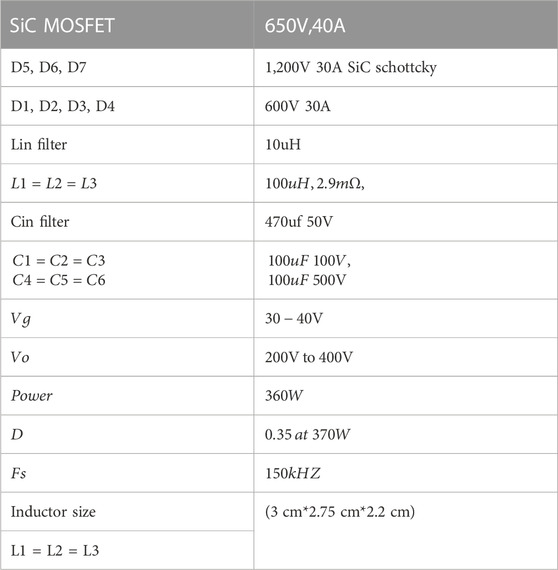
To achieve this, the converter necessitates three small-value inductors and six small-value capacitors. The specific parameter values can be located in Table 1, which outlines the prototype design parameters for the proposed converter. A proposed converter utilizing a high switching frequency has the potential to significantly reduce the size of inductors and capacitors required for its design. As a result, the prototype becomes smaller, lighter, and more cost-effective. To meet the inductor specifications, the converter employs flat wire with remarkably low internal resistance, which greatly minimizes losses. Referring to the inductor specifications in Table 1, it is observed that the internal resistance for all inductors is very small when using flat wire inductors with ferrite cores sized at (3cm 2.75cm 2.2cm).
To design inductors for the proposed converter, we can use Eq. 47 to design inductors L1 and L2. Additionally, Eq. 48 can be used to design inductor L3.
To select the best values of capacitors, we can use Eqs 49–54 to find the values of C1, C2, C3, C4, C5, and C6, respectively. In order to calculate input filter of DC DC converter, Cin filter and Lin filter can be used equation below in Eq. 54.
To calculate the filter volume with respect to the total volume of the converter, the filter volume is 15 cm3, and the total volume of the proposed converter is 185 cm3. Thus, the filter volume in relation to the total volume of the converter is 0.01, accounting for 1% of the total volume.
6 Performance comparison: proposed converter vs. previous high-boost converters
In this section, we conduct a comparative analysis of the proposed converter in contrast to previous DC-DC converters. The simulations for the previous DC-DC converters were performed using Matlab Simulink under identical conditions. From the results depicted in Figure 6A, it is evident that the proposed converter achieves a significantly higher voltage gain when compared to the previous boosting converters. Notably, the proposed converter exhibits a considerable gain at low duty cycles, starting from D = 0.25. This characteristic leads to reduced conduction losses, switching losses, improved overall efficiency, and a notable reduction in the required number of inductors and capacitors. Additionally, Figure 6B reveals that the power MOSFET device in the proposed converter experiences notably lower voltage stress in comparison to the power MOSFET devices utilized in the previously mentioned converters. Moreover, concerning the voltage across diodes, Figure 6C demonstrates that the diodes in the proposed converter are subjected to lower voltage stress when compared to their counterparts in previous converter designs.
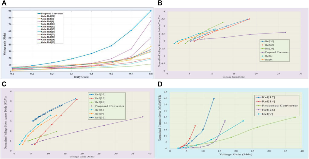
FIGURE 6. (A) Voltage gain of the proposed converter Vs. previous Converters, (B) Voltgae stress across MOSFETs Vs. Voltage gain, (C) Voltage stress across Diode Vs. Voltage gain, (D) Current stress through MOSFET Vs. voltage gain.
Consequently, the suggested converter demonstrates exceptional performance by attaining both a high voltage gain and low voltage stress across power devices, surpassing its predecessors. This is clearly depicted in Figure 6D, where the stress current through the MOSFET in the proposed converter is considerably lower than that experienced by the power MOSFET in prior boosting converters.
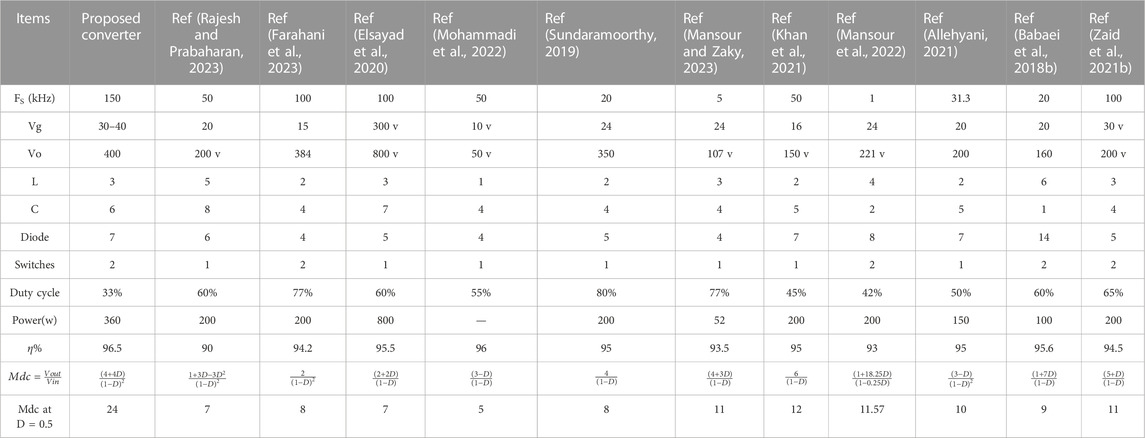
Table 2 presents a comprehensive comparison between the proposed converter and its predecessors, examining various critical factors such as the number of inductors, capacitors, diodes, switching frequency, input current, duty cycle percentage, and MOSFETs utilized in both the new and previous boosting converters.
The innovative design of the proposed converter incorporates a higher switching frequency, resulting in the utilization of smaller inductors and capacitors while effectively reducing parasitic resistance. Consequently, this advancement renders the entire system more compact, lightweight, and cost-efficient. In direct comparison to its forerunners, the proposed converter exhibits superior performance in terms of efficiency, size, and cost-effectiveness. Previously employed boosting converters were capable of elevating low voltage to high voltage ratios, albeit requiring significant high duty ratios. In contrast, the newly devised converter demonstrates remarkable efficiency in elevating low voltage sources to variable output voltage levels ranging from 200V to 400V, necessitating substantially lower duty ratios than its predecessors.
The proposed converter’s distinct advantage lies in its reduced number of power diodes, which leads to minimized losses attributed to forward voltage and internal resistance when juxtaposed with earlier converter models. Moreover, this novel converter boasts a heightened voltage gain, rendering it particularly suitable for renewable energy sources, as it can deliver both variable and fixed high output voltage levels with an extensive range in duty ratio, culminating in an impressive 96.5% efficiency rating.
7 Control strategy of the proposed converter
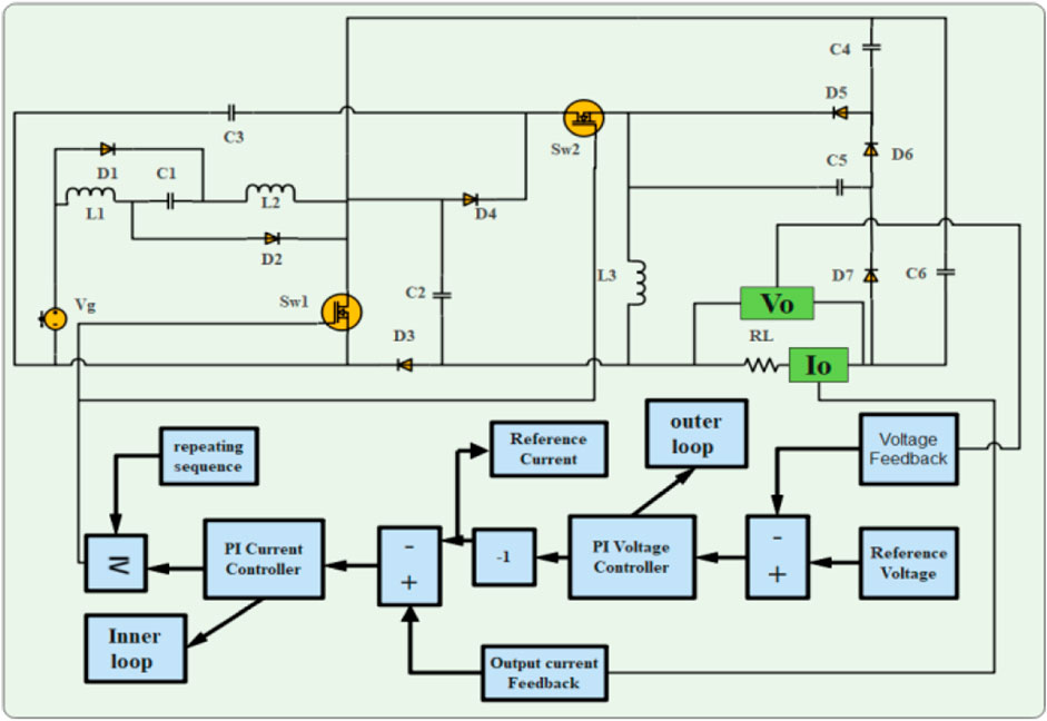
Figure 7 illustrates the proposed converter controller, employing two Proportional Integral (PI) controllers to ensure its effective operation. The initial PI controller functions as an internal controller, stabilizing the load current. Meanwhile, the second PI controller acts as an external controller, responsible for maintaining the desired output voltage. The PI voltage controller operates by taking the discrepancy between the target voltage and the actual output voltage as its input. Using this input, it generates a reference current for the load. To prevent excessive current draw, the reference current is intentionally limited. The disparity between the reference current and the actual current is then fed into the PI current controller, governed by Eq. 55. To properly tune the Ki and Kp parameters of the controller, it is essential for the parameters of the PI voltage controller to be faster than those of the PI current controller. This measure guarantees that the steady-state error remains at zero.
Figure 8A portrays the dynamic adaptability of the proposed converter, exemplifying its capacity to vary the output voltage while maintaining a constant input voltage, thus catering to diverse application demands. Similarly, in Figure 8B, the stability of the proposed converter’s output is depicted, illustrating its ability to remain constant even when subjected to varying load conditions throughout the day, while maintaining a consistent input voltage. Moreover, Figure 8C presents compelling evidence of the proposed converter’s exceptional performance, as it demonstrates its proficiency in supplying a stable output voltage despite fluctuations in the input voltage. This remarkable attribute is achieved through the implementation of a voltage and current PI-controller for the converter, facilitating swift and precise responses to varying conditions.

FIGURE 8. (A) Variable output voltage of the proposed Converter at fixed input Voltage (B) fixed output voltage at changing load current (C) fixed output voltage at changing input voltage.
Significantly, the proposed converter exhibits an impressive power density, owing to its broader range of duty ratios. This distinctive feature renders it exceptionally well-suited for applications requiring a consistently high fixed output voltage. Overall, the amalgamation of these remarkable characteristics establishes the proposed converter as an exemplary and versatile solution for a wide array of practical applications.
8 Proposed converter efficiency calculation
The proposed converter comprises three inductors, six capacitors, two power switches, and seven diodes. While these components are integral to the converter’s functionality, it is important to acknowledge that they are not ideal. Each inductor, for example, possesses an inherent internal resistance. Similarly, the capacitors exhibit equivalent series resistances denoted by rc. Notably, the power diode entails two types of power losses—one due to its internal resistance and the other due to its forward voltage Vf. Additionally, the power MOSFET devices contribute to power losses through conduction and switching processes. Consequently, a comprehensive evaluation of the proposed converter must account for all these losses. For a visual reference, Figure 9 depicts the internal resistances of both active and passive elements.
Eq. 56 is the general equation for calculating the RMS current.
In order to calculate the RMS current through power MOSFETs, Eqs 57, 58 can be used to describe the RMS current flowing through MOSFETs. Additionally, Eqs 59–65 can be utilized to calculate the RMS current through diodes.
To determine the RMS current through inductors L1, L2, and L3, you can use Eqs 66, 67 respectively. Meanwhile, the RMS current through capacitors can be obtained by utilizing Eqs 68–73.
8.1 Quantifying conduction and switching losses in power MOSFETs
In this section, we perform calculations for both conduction and switching losses of the MOSFETs used in the proposed converter. The MOSFET’s on-resistance (Ron) plays a crucial role in determining the system’s performance. A lower Ron value is highly desirable as it leads to increased voltage gain and reduces losses associated with power MOSFETs during conduction and switching processes.
To evaluate the conduction and switching losses of the power MOSFETs, we can employ Eqs 74, 75 to deduce the power conduction losses of Sw1 and Sw2, referred to as Pcd1 and Pcd2, respectively. Furthermore, Eq. 76 allows us to determine the power switching losses, denoted as PSWL, for MOSFETs. Switching losses can be calculated by considering half of the voltage stress on the MOSFET, output capacitor Co, and the switching frequency Fs. By integrating Eqs 74, 75, 77, 78, we arrive at a comprehensive Eq. 79 to ascertain the total power losses of MOSFETs, denoted as TPLCS1,2.
8.2 Calculation of power losses in all diodes
In this section, the power losses in a diode are attributed to its internal resistance (rd) and the forward voltage (Vf). To determine the power losses caused by Vf as in Eq. 82, it is essential to calculate the average diode current first, which can be achieved using Eq. 80. Once the average current through the diodes is obtained, multiplying it by Vf yields the power losses (Pvf) due to the forward voltage. On the other hand, if the diode power losses due to rd need to be determined, Eq. 81 can be utilized. To obtain the total power losses (TPDL) across all seven diodes, the summation of all power losses in the diodes can be done using Eq. 83.
8.3 Total power losses in inductor and capacitors
Power losses occur in inductors and capacitors due to their internal resistance. Therefore, using inductors with low internal resistance in the proposed converter can increase efficiency and reduce losses. The power losses associated with inductors (PL) and capacitors (PC) can be determined using Eqs 84, 85, respectively.
The losses encountered in the proposed converter can be categorized into four main groups: MOSFET losses, diode losses, capacitor losses, and inductor losses. To ascertain the overall power loss (TPLPC) of the converter, Eq. 86 can be employed, which involves summing up the power losses of the power MOSFETs (TPLCS), the total power losses of the diodes (TPDL), and the losses in the inductors (TPL) and capacitors (TPC). The efficiency of the proposed converter can be evaluated using Eq. 87.
9 Simulation and experimental results and discussions
In this section, we developed a prototype design of a 360 W converter to validate the accuracy of both simulation and experimental outcomes, as shown in Figure 10A.
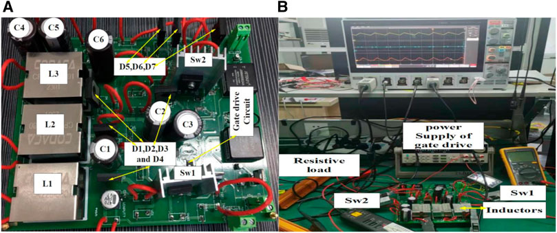
FIGURE 10. (A) PCB prototype of the proposed Converter (B) experimental test of the proposed converter.
The converter was subjected to rigorous evaluation in a laboratory environment, as depicted in Figure 10B. To further validate the laboratory results across diverse conditions, MATLAB and PLECS software were employed. It’s important to note that the converter integrated non-ideal inductors and capacitors, and all parasitic resistances were taken into account in the proposed DC-DC converter design.
Figure 11A shows the inductor current when the proposed converter operates in CCM. Figure 11B displays the voltage across the inductor during the on and off states. It can be observed that the voltage across L3 is very small, equating to half of the output voltage. In Figure 11C, it is evident that the proposed converter can supply 360 W at a load current of 0.91 A and an output voltage of 400 V, with a gain of (Mdc = 13.3).
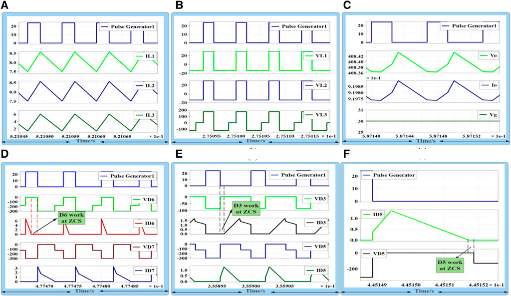
FIGURE 11. (A) IL1, IL2, IL3 at CCM (B) voltage across inductors,VL1, VL2, VL3 (C) output voltage 400 V and load current 0.91 A at Vg = 30 V (D) VD6 and ID6 at ZCS, VD7, and ID7 at DCM2, (E) VD3, ID3 at ZCS, VD5, ID5 at ZCS at DCM2, (F) ID5, VD5 at ZCS at CCM.
From Figure 11D, it can be seen that the voltage across D6 and the current through D6 operate at ZCS when capacitor C4 becomes zero at (α). Figure 11E illustrates the voltage across D3 and the current through D3 when D3 operates at ZCS. Additionally, the current through D5 operates at ZCS when the proposed converter is in DCM2. In Figure 11F, it is apparent that D5 operates at ZCS when the proposed converter operates in CCM.
In terms of the experimental results, the proposed converter was designed and tested to verify its high voltage gain. In Figure 12A, the inductor currents of L1 and L2 are shown, and both of them operate in (CCM). Figure 12B displays the inductor currents of L1 and L3, where L3 operates in (DCM) under a load current of 0.91 A, 400 V output voltage, and 360 W load.
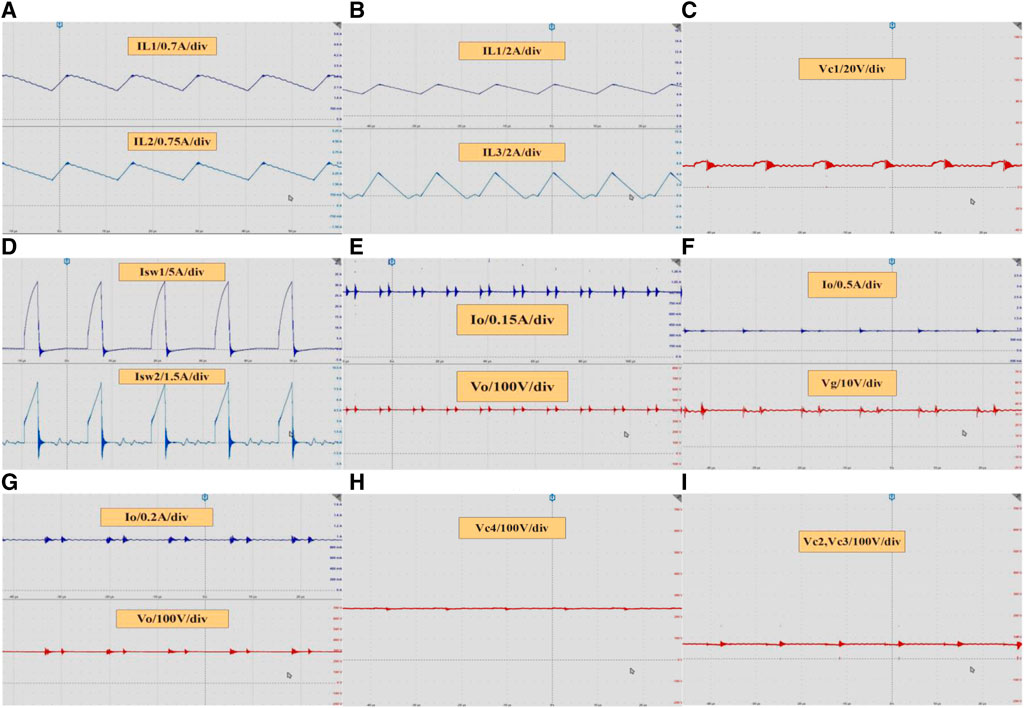
FIGURE 12. (A) IL1, IL2, (B) IL1, IL3 at DCM (C) Vc1, (D) Isw1, Isw2, (E) Io = 0.91 at Vo = 400 V, (F) Io = 0.91, Vg = 32 V, (G) Io = 1A, Vo = 300 V, (H) Vc4 = 250 V, (I) Vc2 = Vc3 = 85 V.
Moving on to Figure 12C, it illustrates the voltage across C1, which is equal to the input voltage. Figure 12D shows the current through the power MOSFETs when the proposed converter supplies a 360 W load. In Figure 12E, we can observe the load current of 0.91 A at a load voltage of 400 V and an input voltage of 32 V, as depicted in Figure 12F.
Additionally, the proposed converter can supply a variable load voltage of 300 V at 1 A, as demonstrated in Figure 12G, where the voltage across C4 is equal to 250 V, and the voltages across C2 and C3 are equal to 85 V, as shown in Figure 12H.
Overall, a DC-DC converter represents a significant advancement in the field, combining outstanding voltage gain, high efficiency, and reliability. Its simple structure, reduced component count, and effective management of voltage stress make it an appealing choice for various applications requiring high voltage conversion.
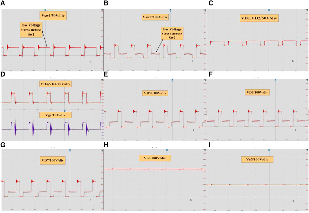
From Figure 13A, we observe that the voltage across SW1 is very small at high load voltage. Additionally, Figure 13B shows the voltage across Sw2, which also remains very small when the load voltage is equal to 400 V. Figure 13C displays the voltage across D1 and D2, which is equal to the input voltage. In Figure 13D, we can observe the voltage across D3 and D4. In Figures 13E–G, we can see the voltage across D5, D6, and D7 respectively. Turning to Figure 13H, the voltage across C6 is visible, and in Figure 13I, we can see the voltage across C5.
From Figure 14A, we can observe the current through D7 in DCM and the current through capacitor C1 during on and off state. In Figure 14B, we can see the current through D5 and D6 in DCM1. Figure 14C shows the current through D3 and the voltage across D3, with D3 operating at ZCS. Figure 14D allows us to observe the current through C5 and C6 in DCM1. Finally, from Figure 14E, we can see the current through capacitor C4 and C2 when the proposed converter operates in DCM1, with a load current of 0.9 A, 400 V output voltage, and 360 W power. Figure 14F it can see the Dynamic response of the proposed converter at changing the load from 200 to 300 W at fixed load voltage.
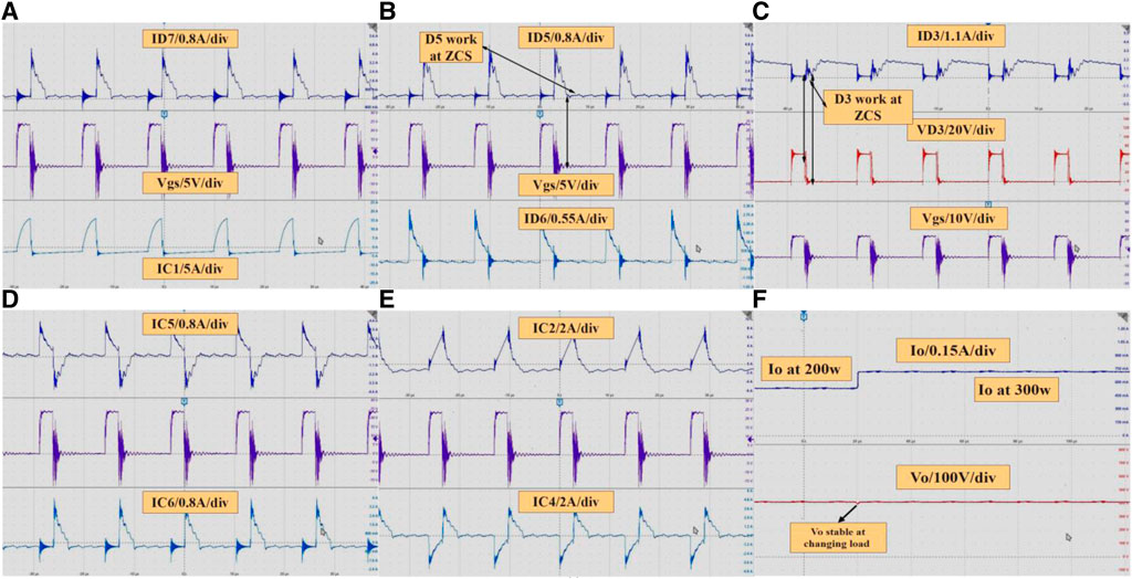
FIGURE 14. (A) ID7, Ic1, (B) ID5, ID6, (C) ID3, VD3, (D) IC5, IC6 at DCM1, (E) IC2, IC4 at DCM1 (F) Dynamic response of the proposed converter at changing the load from 200 to 300 W at fixed load voltage.
From Figure 15A it can see that the proposed converter archive high efficiency at high load current. In addition, the proposed converter can supply high load voltage at low duty cycle as shown in Figure 15B. Figure 15C it can see the efficiency of the proposed converter at output load power at different input voltage.
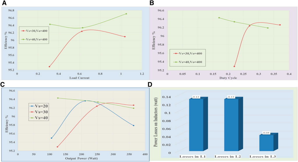
FIGURE 15. Efficiency of the proposed converter measured (A) efficiency Vs. Load current,(B) efficiency Vs. duty cycle (C) efficiency Vs. power (D) power losses of the flat wire inductors.
In Figure 15D, the graph depicts the power losses of flat wire inductors under the operation of the suggested converter while catering to a 360 W load. Evidently, the power losses exhibited by these inductors are notably minimal after using inductors with low internal resistance. This observation underscores the efficient and high-performance operation of the suggested converter.
The proposed converter achieved a higher voltage gain than previous converters and can supply a variable high output voltage at a very low duty ratio compared to previous converters. Specifically, the proposed converter achieves an efficiency of 96.5% when the input voltage is 30 V, and the output voltage is 400 V at a duty ratio of 33%. The proposed converter can supply loads greater than 360 W while maintaining high efficiency. Additionally, the diode of MTB D5 operates at ZCS when the converter operates in DCM, and the capacitor charge becomes zero at (β). Moreover, D5 operates at ZCS when the proposed converter operates in CCM while supplying high current. Furthermore, the diode of MTB D6 operates at ZCS when the capacitor charge becomes zero at (α). Moreover, the diode of MVM D3 operates at ZCS at time (δ). By incorporating WBG power MOSFETs and power diodes into the converter’s design, it exhibits exceptional performance and efficiency. Additionally, the implementation of a high switching frequency allows for significant reductions in the values of inductors and capacitors, resulting in a compact and lightweight converter design. Consequently, the proposed converter surpasses its predecessors by achieving higher voltage gain, while the power MOSFETs and power diodes experience reduced voltage stress compared to conventional boosting converters. Moreover, the proposed converter offers the ability to supply high load currents at variable output voltages, accommodating a wide range of duty ratios. Its enhanced efficiency, surpassing that of previous DC-DC converters, further establishes its high-performance capabilities.
The described converter is capable of providing a maximum power output of 360 W at an output voltage of 400 V with high efficiency. Furthermore, it is well-suited for applications demanding elevated output voltage, such as LED street lights and specific medical equipment. The design considerations encompass aspects like input current, available input voltage, converter efficiency, thermal management, and component ratings.
However, as power demand escalates, certain limitations come into play. At higher power levels, the converter’s components might experience heightened stress, potentially resulting in overheating, decreased efficiency, and compromised overall reliability. To address these concerns, the proposed converter boasts the flexibility to deliver varying output voltages tailored to specific applications. Additionally, it excels at efficiently transforming low input voltages into high output voltages, effectively achieving the 360 W output.
To effectively manage these challenges and maintain optimal performance, careful attention must be paid to factors such as thermal management, prudent component selection, and meticulous system design when upscaling power requirements. This approach will effectively mitigate the risks linked with intensified component stress and ensure continued efficient and reliable operation, even when confronted with elevated power demands.
10 Conclusion
A DC-DC converter employs a modified triple-boosting architecture, interleaved with modified switched inductor capacitors, to achieve ultra-high voltage gain in photovoltaic applications. The simulation results of the proposed converter were verified by fabricating a 360 W PCB. A comparison was made between the proposed converter and previous boosting converters. The proposed converter achieved a higher voltage gain than previous converters and can supply a variable high output voltage at a very low duty ratio compared to previous converters. Specifically, the proposed converter achieves an efficiency of 96.5% when the input voltage is 30 V, and the output voltage is 400 V at a duty ratio of 33%. The proposed converter can supply loads greater than 360 W while maintaining high efficiency. Additionally, the diode of MTB D5 operates at ZCS when the converter operates in DCM, and the capacitor charge becomes zero at (β). Moreover, D5 operates at ZCS when the proposed converter operates in CCM while supplying high current. Furthermore, the diode of MTB D6 operates at ZCS when the capacitor charge becomes zero at (α). Moreover, the diode of MVM D3 operates at ZCS at time (δ).
In summary, the development of this novel converter exemplifies the immense potential for achieving high voltage gain and addresses the challenges associated with efficient energy conversion in photovoltaic systems. Further exploration and experimentation in this field hold the promise of even more efficient and effective converter designs for renewable energy applications.
Data availability statement
The raw data supporting the conclusion of this article will be made available by the authors, without undue reservation.
Author contributions
AA: Formal Analysis, Methodology, Software, Writing–original draft. XW: Conceptualization, Supervision, Writing–review and editing. HA: Writing–review and editing. K: Funding acquisition, Writing–review and editing. MK: Funding acquisition, Writing–review and editing.
Funding
The author(s) declare that no financial support was received for the research, authorship, and/or publication of this article.
Conflict of interest
The authors declare that the research was conducted in the absence of any commercial or financial relationships that could be construed as a potential conflict of interest.
Publisher’s note
All claims expressed in this article are solely those of the authors and do not necessarily represent those of their affiliated organizations, or those of the publisher, the editors and the reviewers. Any product that may be evaluated in this article, or claim that may be made by its manufacturer, is not guaranteed or endorsed by the publisher.
References
Abbasi, M., and Lam, J. (2019). A modular SiC-based step-up converter with soft-switching-assisted networks and internally coupled high-voltage-gain modules for wind energy system with a medium-voltage DC-grid. IEEE J. Emerg. Sel. Top. Power Electron. 7 (2), 798–810. doi:10.1109/jestpe.2019.2900281
Abbasian, S., Farsijani, M., and Hafezi, H. (2022, September). A double-switch high gain DC-DC converter based on coupled-inductors. In Proceedings of the 2022 international conference on smart energy systems and technologies (SEST) ,Eindhoven, Netherlands (pp. 1–6).
Allehyani, A. (2021). Analysis of A transformerless single switch high gain DC–DC converter for renewable energy systems. Arabian J. Sci. Eng. 46 (10), 9691–9702. doi:10.1007/s13369-021-05472-3
Ardi, H., and Ajami, A. (2018). Study on a high voltage gain SEPIC-based DC–DC converter with continuous input current for sustainable energy applications. IEEE Trans. power Electron. 33 (12), 10403–10409. doi:10.1109/tpel.2018.2811123
Azizkandi, M. E., Sedaghati, F., Shayeghi, H., and Blaabjerg, F. (2019). A high voltage gain DC–DC converter based on three winding coupled inductor and voltage multiplier cell. IEEE Trans. Power Electron. 35 (5), 4558–4567. doi:10.1109/tpel.2019.2944518
Babaei, E., Maheri, H. M., Sabahi, M., and Hosseini, S. H. (2018a). Extendable nonisolated high gain DC–DC converter based on active–passive inductor cells. IEEE Trans. industrial Electron. 65 (12), 9478–9487. doi:10.1109/tie.2018.2807367
Babaei, E., Maheri, H. M., Sabahi, M., and Hosseini, S. H. (2018b). Extendable nonisolated high gain DC–DC converter based on active–passive inductor cells. IEEE Trans. industrial Electron. 65 (12), 9478–9487. doi:10.1109/tie.2018.2807367
Das, M., and Agarwal, V. (2016). Design and analysis of a high-efficiency DC–DC converter with soft switching capability for renewable energy applications requiring high voltage gain. IEEE Trans. Industrial Electron. 63 (5), 2936–2944. doi:10.1109/tie.2016.2515565
Dhananjaya, M., Vellingiri, M., Alaas, Z. M., Rawa, M., Sathik, M. J., Almakhles, D., et al. (2023). New multi-source DC-DC boost converter and its generalized structure with experimental validation. Ain Shams Eng. J., 14(10), 102173. doi:10.1016/j.asej.2023.102173
Elsayad, N., Moradisizkoohi, H., and Mohammed, O. (2020). A new SEPIC-based step-up DC-DC converter with wide conversion ratio for fuel cell vehicles: analysis and design. IEEE Trans. industrial Electron. 68 (8), 6390–6400. doi:10.1109/tie.2020.3007110
Farahani, H. J., Rezvanyvardom, M., and Mirzaei, A. (2023). Non-isolated high step-up DC–DC converter based on switched-inductor switched-capacitor network for photovoltaic application. IET Generation, Transm. Distribution 17 (3), 716–729. doi:10.1049/gtd2.12700
Fardahar, S. M., and Sabahi, M. (2019). New expandable switched-capacitor/switched-inductor high-voltage conversion ratio bidirectional DC–DC converter. IEEE Trans. Power Electron. 35 (3), 2480–2487. doi:10.1109/tpel.2019.2932325
Folmer, S., and Stala, R. (2021). DC-DC high voltage gain switched capacitor converter with multilevel output voltage and zero-voltage switching. IEEE Access 9, 129692–129705. doi:10.1109/access.2021.3111546
Gu, Y., Chen, Y., Zhang, B., Qiu, D., and Xie, F. (2018). High step-up DC–DC converter with active switched <italic>LC</italic>-Network for photovoltaic systems. IEEE Trans. Energy Convers. 34 (1), 321–329. doi:10.1109/tec.2018.2876725
Hasanpour, S. A. R. A., Siwakoti, Y. P., and Blaabjerg, F. R. E. D. E. (2023). A new soft-switched high step-up trans-inverse DC/DC converter based on built-in transformer. IEEE Open J. Power Electron. 4, 381–394. doi:10.1109/ojpel.2023.3275651
Hasanpour, S., Forouzesh, M., Siwakoti, Y. P., and Blaabjerg, F. (2021). A new high-gain, high-efficiency SEPIC-based DC–DC converter for renewable energy applications. IEEE J. Emerg. Sel. Top. Industrial Electron. 2 (4), 567–578. doi:10.1109/jestie.2021.3074864
Khan, S., Zaid, M., Mahmood, A., Nooruddin, A. S., Ahmad, J., Alghaythi, M. L., et al. (2021). A new transformerless ultra high gain DC–DC converter for DC microgrid application. IEEE Access 9, 124560–124582. doi:10.1109/access.2021.3110668
Kumar, G. G., Sundaramoorthy, K., Karthikeyan, V., and Babaei, E. (2020). Switched capacitor–inductor network based ultra-gain DC–DC converter using single switch. IEEE Trans. Industrial Electron. 67 (12), 10274–10283. doi:10.1109/tie.2019.2962406
Li, F., He, J., Huang, D., Luo, P., Jiang, H., and Hu, N. (2023). Nitrogen retention and emissions during membrane-covered aerobic composting for kitchen waste disposal. IEEE Trans. Industrial Electron., 1–31. doi:10.1080/09593330.2023.2252162
Mansour, A. S., Amer, A. H. H., El-Kholy, E. E., and Zaky, M. S. (2022). High gain DC/DC converter with continuous input current for renewable energy applications. Sci. Rep., 12(1), 12138. doi:10.1038/s41598-022-16246-8
Mansour, A. S., and Zaky, M. S. (2023). A new extended single-switch high gain DC–DC boost converter for renewable energy applications. Sci. Rep., 13(1), 264. doi:10.1038/s41598-022-26660-7
Mirzaee, A., and Moghani, J. S. (2019). Coupled inductor-based high voltage gain DC–DC converter for renewable energy applications. IEEE Trans. Power Electron. 35 (7), 7045–7057. doi:10.1109/tpel.2019.2956098
Mohammadi, F., Gharehpetian, G. B., Rastegar, H., and Farhadi-Kangarlu, M. (2022). Switched capacitor cell-based non-isolated step-up converter. CSEE J. Power Energy Syst.
Pashaie, R., Sabahi, M., and Babaei, E. (2023). An interleaved high step-down coupled inductor based quadratic DC-DC converter. IET Power Electron. 16, 1558–1572. doi:10.1049/pel2.12496
Premkumar, M., Kumar, C., and Sowmya, R. (2019). Analysis and implementation of high-performance DC-DC step-up converter for multilevel boost structure. Front. Energy Res. 7, 149. doi:10.3389/fenrg.2019.00149
Rahimi, R., Habibi, S., Ferdowsi, M., and Shamsi, P. (2021). An interleaved high step-up DC-DC converter based on integration of coupled inductor and Built-in-Transformer with switched-capacitor cells for renewable energy applications. IEEE Access 10, 34–45. doi:10.1109/access.2021.3138390
Rahimi, R., Habibi, S., Shamsi, P., and Ferdowsi, M. (2022). A three-winding coupled-inductor-based dual-switch high step-up DC–DC converter for photovoltaic systems. IEEE J. Emerg. Sel. Top. Industrial Electron. 3 (4), 1106–1117. doi:10.1109/jestie.2022.3151554
Rajesh, R., and Prabaharan, N. (2023). Design of new nonisolated high gain converter for higher power density. Int. Trans. Electr. Energy Syst. 2023, 1–10. doi:10.1155/2023/2011926
Shaw, P., and Sahoo, M. (2018, December). Switched-inductor based high voltage gain step-up DC-DC converter for photovoltaic micro-inverter application. In Proceedings of the 2018 15th IEEE India council international conference (INDICON) ,Coimbatore, India (pp. 1–6).
Singh, A. K., Mishra, A. K., Gupta, K. K., and Siwakoti, Y. P. (2022). High voltage gain bidirectional DC-DC converters for supercapacitor assisted electric vehicles: A review. CPSS Trans. Power Electron. Appl. 7 (4), 386–398. doi:10.24295/cpsstpea.2022.00035
Sundaramoorthy, K. (2019, December). Switched inductor-capacitor network based non-isolated DC-DC converter: A double 2 gain converter with single switch. In Proceedings of the 2019 national power electronics conference (NPEC) ,Tiruchirappalli, India (pp. 1–6).
Veerachary, M., and Sen, P. (2022). Dual-switch enhanced gain boost DC–DC converters. IEEE Trans. Industry Appl. 58 (4), 4903–4913. doi:10.1109/tia.2022.3171533
Zaid, M., Khan, S., Siddique, M. D., Sarwar, A., Ahmad, J., Sarwer, Z., et al. (2021a). A transformerless high gain dc–dc boost converter with reduced voltage stress. Int. Trans. Electr. Energy Syst. 31 (5), e12877. doi:10.1002/2050-7038.12877
Keywords: triple boost technique, ZCS, DC-DC converter, switched capacitator, switched indcutor circuit
Citation: Algamluoli A, Wu X, Abdulhadi HM, Kitmo and Khan MA (2023) Ultra high voltage gain non-isolated DC-DC converter based on new interleaved triple boosting technique. Front. Energy Res. 11:1273155. doi: 10.3389/fenrg.2023.1273155
Received: 05 August 2023; Accepted: 28 August 2023;
Published: 11 September 2023.
Edited by:
Amjad Ali, King Fahd University of Petroleum and Minerals, Saudi ArabiaReviewed by:
Van-Dai Bui, Kyungpook National University, Republic of KoreaMohammad Ali, King Fahd University of Petroleum and Minerals, Saudi Arabia
Copyright © 2023 Algamluoli, Wu, Abdulhadi, Kitmo and Khan. This is an open-access article distributed under the terms of the Creative Commons Attribution License (CC BY). The use, distribution or reproduction in other forums is permitted, provided the original author(s) and the copyright owner(s) are credited and that the original publication in this journal is cited, in accordance with accepted academic practice. No use, distribution or reproduction is permitted which does not comply with these terms.
*Correspondence: Ammar Algamluoli, YW1tYXIuYWxnYW1sdW9saUBjb2VuZy51b2JhZ2hkYWQuZWR1Lmlx; Xiaohua Wu, d3hoQG53cHUuZWR1LmNu; Kitmo, a2l0bW9iYWhuQGdtYWlsLmNvbQ==
 Ammar Algamluoli
 Xiaohua Wu1*
 Haider M. Abdulhadi
 Kitmo
Kitmo