 Dai Wan1,2
 Jingtao Xu
95% of researchers rate our articles as excellent or good
Learn more about the work of our research integrity team to safeguard the quality of each article we publish.
Find out more
ORIGINAL RESEARCH article
Front. Energy Res. , 03 August 2023
Sec. Smart Grids
Volume 11 - 2023 | https://doi.org/10.3389/fenrg.2023.1241718
This article is part of the Research Topic Coordination and Control of Power Converters in Modern Power Systems View all 10 articles
A current observer-based digital critical conduction mode control of a bidirectional DC–DC converter with full-range soft switching for battery charging/discharging applications is proposed in this paper. Under the proposed control method, the bidirectional DC/DC converter operates in the critical continuous mode (CRM), the full-range zero-voltage switching (ZVS) can be achieved, and the inductor current ripple can be optimized. The CRM control is achieved by the proposed current observer, and the zero-crossing detection (ZCD) analog circuit or current sampling circuit can be eliminated. Therefore, compared with existing methods, the design complexity of the hardware circuit can be simplified. In addition, the proposed current observer can estimate the inductor current over a wide range of load and voltage variations. Therefore, the proposed control method can be applied to a wide range of charging and discharging applications. Finally, a prototype with 30–60 V input voltage, 24 V output voltage, and 75–150 kHz switching frequency is built. The experimental data and waveforms prove the correctness and advantages of the solutions proposed in this paper.
With the improvement of power electronics technology and energy storage, the DC microgrid has also been developed rapidly. As one of the cores, the bidirectional DC/DC converters are widely used in new energy power generation and battery charging and discharging applications (Premkumar et al, 2019; Chen et al, 2022; Lu et al, 2022; Madhana and Mani, 2022; Fang et al, 2023; Samad et al, 2023). Due to the simple circuit structure and control strategy, the bidirectional buck/boost circuit is one of the most popular DC/DC converters (Li et al., 2023; Lan et al, 2022). In order to reduce the size of the filter and improve the power density of the system, the converter needs to be operated at a higher switching frequency (Marxgut et al, 2014; Reusch and Strydom, 2015; Tao et al, 2021; Cai et al, 2022). However, under the traditional control methods, the bidirectional buck/boost converter operates in the hard switching state. The increase in switching frequency will lead to a significant increase in switching losses, and the conversion efficiency will be decreased. Therefore, the converter topology structure and control method can be improved to optimize the conversion efficiency of the converter.
The realization of soft switching can effectively reduce switching loss and electromagnetic interference (EMI), which is helpful in improving the switching frequency of the converter. Adding an auxiliary resonant network is an effective method to achieve ZVS (Pattnaik et al, 2010; Lee, 2014; Basharat et al, 2021; Hajiheidari et al, 2021). The resonant current flows through the body diode of the MOSFET, which can reduce the drain-source voltage of the MOSFET to zero before it is turned on. Adding the auxiliary switches to achieve ZVS for the main switches is another approach (Chuang and Ke, 2008; Rodrigues et al, 2009; Chuang, 2010; Mohammadi, 2020). Although adding auxiliary devices can enable the converter to achieve soft switching, the overall complexity and volume of the circuit are increased.
In addition to the topology improvement, the optimization of control strategies is also effective. The topology of the bidirectional buck/boost converter is shown in Figure 1 (Sable et al, 1992; Deng et al, 2004; Ji et al, 2017; Sha et al, 2022). When the bidirectional buck/boost converter operates in the critical continuous mode (CRM), the inductor current will reverse during each switching cycle, and all switches can achieve ZVS (Ren et al, 2020; Wang et al, 2021). In addition, under CRM, the inductor current ripple can be minimized. In order to realize CRM control for the bidirectional buck/boost converter, the switching frequency needs to be adjusted according to different load and voltage variations. Usually, the zero-crossing detection analog circuits are used to control the turning-on and turning-off of the freewheeling MOSFET (Lai and Chen, 1993; Hu et al, 2014). In addition, there are many dedicated ZCD chips to achieve CRM control of the converter, which can further improve the integration of the converter. However, the analog detection circuits are sensitive to sampling noise, which could lead to the incorrect operation of MOSFETs. At present, digital power supply is gaining popularity, and the analog scheme will be limited. Hence, many digital CRM control strategies (Baek et al, 2013; Liu et al, 2020), which are more flexible, are proposed. Usually, in digital control, the inductor current or input and output currents need to be sampled to obtain power information, and then the optimal switching frequency is calculated according to the sampling value. Due to the simple circuit structure and computational complexity, the digital CRM control can be achieved more conveniently and flexibly. However, in the existing digital CRM control strategies, the high-precision current sensor is necessary, which is relatively expensive, and the overall volume is also increased.
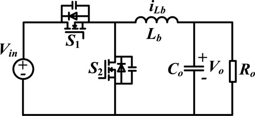
FIGURE 1. Bidirectional buck/boost converter.
A current observer-based CRM control is proposed in this paper. The traditional detection and sampling circuits are replaced by the proposed current observer. Hence, only the voltage sampling at the input and output terminals is required. The proposed solution has the following two main advantages:
1) The proposed CRM control method can achieve full-range ZVS without any current sensor or ZCD circuit. Hence, the circuit complexity and the sampling noise sensitivity are reduced.
2) The proposed current observer can accurately estimate the average value of the inductor current over a wide range of load and voltage variations, which is suitable for a wide range of charging and discharging applications.
The working principles of forward transmission and reverse transmission are similar, and the former is analyzed in detail in this paper. As shown in Figure 1, the MOSFETs S1 and S2 of the bidirectional buck/boost converter work in complementary conduction. The output voltage Vo can be controlled by the MOSFETs. Ds1 is defined as the duty cycle of the upper switch S1. The bidirectional buck/boost converter operates in the critical continuous mode. Hence, the inductor current will reverse during each switching cycle, and both S1 and S2 can achieve ZVS soft switching. The working waveforms of the bidirectional buck/boost converter under the critical continuous mode are shown in Figure 2.
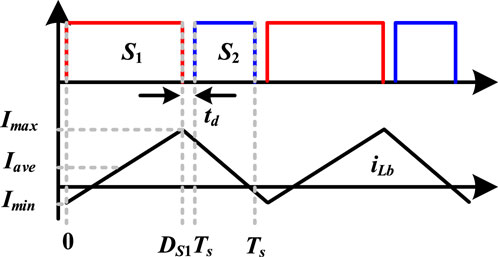
FIGURE 2. Working waveforms of the bidirectional buck/boost converter under the critical continuous mode.
Under CRM, the inductor current could be reversed; hence, the minimum value of filter inductor current Imin is lower than zero. Before S1 conduction, all MOSFETs are turned off due to the dead time, and the filter inductor current will flow through the body diode of the MOSFET S1. At time 0, S1 can achieve zero-voltage soft switching. During the duration of [0- Ds1Ts], the filter inductor current will rise to its maximum value Imax. After S1 is turned off, the filter inductor current will also flow through the body diode of the MOSFET S2. Hence, S2 can also be turned on with ZVS.
Based on the analysis, at forward transmission, the maximum value of the filter inductor current Imax must be higher than zero; hence, the MOSFET S2 must realize ZVS. However, the minimum value of the filter inductor current might be higher than zero, and S1 might lose ZVS. Therefore, the peak-to-peak value of the filter inductor current should be twice higher than its average value:
where Pt represents the transmission power.
In order to ensure sufficient energy to complete the charging and discharging of the MOSFET output capacitor, the valley current needs to be satisfied:
where Coss is the output capacitance of MOSFET.
In addition, because the dead time is relatively short, the inductor current can be approximately equivalent to a constant current source within the dead time. The dead time Td also needs to be long enough to ensure the realization of ZVS, which can be expressed as
According to (Eq. 1) and the voltage-second balance principle, the soft-switching condition for the MOSFET S1 can be expressed as
According to (Eq. 4), it can be seen that when the transmission power and switching frequency are high, it is difficult to achieve ZVS. Therefore, the filter inductance needs to be small enough to ensure ZVS. However, a smaller filter inductance will lead to a higher circulating current and conduction loss. Therefore, it is necessary to design an appropriate filter inductance based on the working conditions, as shown in Figure 3. In order to ensure the full load range of ZVS, it is necessary to design Lb under the full load and minimum frequency. In Figure 3A, below the surface lies the ZVS region. In order to ensure the ZVS and optimize the circulating current, the inductance value can be designed as a boundary value. The 2D graph of boundary inductance values under different input voltages is shown in Figure 3B. It can be seen that when the input voltage is low, the inductance boundary value is low.
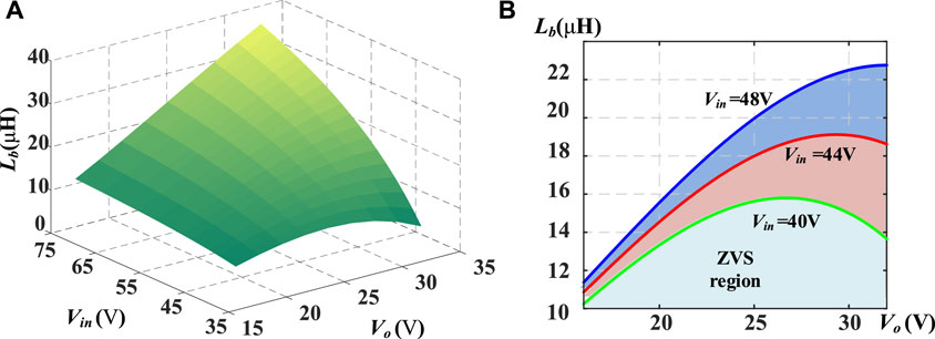
FIGURE 3. ZVS region. (A) Three-dimensional graph. (B) Two-dimensional graph.
After designing the filter inductor, it is necessary to adjust the switching frequency based on the working voltage and power to achieve CRM, as shown in Figure 4. When the load is light, Imin will be much lower than zero, and the circulating current will be higher, so it is necessary to increase the switching frequency. On the other hand, when Imin is above zero, the ZVS soft switching will be lost, so the switching frequency needs to be reduced. After adjusting the switching frequency, Imin will be slightly below zero, and the converter will operate in the critical conduction mode.
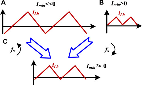
FIGURE 4. Switching frequency regulation for the critical conduction mode. (A) fs is too low. (B) fs is too high. (C) fs is appropriate.
Based on the ZVS condition (Eq. 4), the optimal switching frequency for CRM operation can be derived as
According to (Eq. 5), it can be seen that in order to adjust the switching frequency, it is necessary to sample the input and output voltages and the average value of the filter inductor current. However, high-precision current sensors and sampling circuits are usually more expensive. Therefore, this paper proposes a CRM control method based on the current observer, which can save current sensors and reduce hardware circuit complexity.
In order to observe the inductance current in a wide load range, a load adaptive current observer needs to be designed. The state equation of the switching average model for the bidirectional buck/boost converter can be expressed as
where rL is the parasitic resistor of the filter inductor.
The designed current observer can be expressed as
where gn(n=1,2,3) is the observer coefficient.
The error of the observed variables can be expressed as
Substituting formula (6) and Eq. 8 into formula (8), the state equation of the observation variables error can be expressed as
The Lyapunov function for observed variable errors can be written as
The derivative of function (Eq. 10) can be derived as
In order to stabilize the observer, formula (11) must converge to zero. Therefore, the designed observer coefficients can be derived as
Finally, the designed filter inductor current observer can be expressed as
According to (14), the observer block diagram can be drawn as shown in Figure 5. Only the input voltage and output voltage need to be sampled. g1, g2, and g3 are parameters of the observer, which can be designed according to (Eq. 12). In the proposed observer, besides the observation equations of output capacitor voltage vo and inductance current iLb, there is also the observation equation of load θ. The proposed observer can adaptively observe the filter inductor current average value when the load varies in a wide range.

FIGURE 5. Observer block diagram.
After the filter inductor current is observed, according to the CRM working conditions, the optimal inductor current ripple can be calculated, which is approximately equal to 2Iave. Therefore, the optimal switching frequency can also be calculated.
The flow chart of the proposed CRM control is shown in Figure 6, which mainly includes the following three steps:
1) Vin and Vo are obtained through the voltage sensor.
2) Based on the designed current observer, Iave can be obtained.
3) The switch frequency is adjusted according to formula (5).
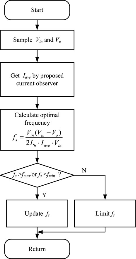
FIGURE 6. Flow chart of the current observer-based CRM control.
The proposed CRM control method does not require a current sensor. The method proposed in this paper is cost-effective and easy to achieve because of the absence of ZCD or a current sensor.
The control block diagram is depicted in Figure 7. The converter adopts the traditional single-voltage loop PI control to control the output voltage constant. The proposed observer is applied to estimate the filter inductor current. Finally, fs can be derived from the proposed CRM control strategy. Under the proposed control strategy, the full range ZVS and the lowest current ripple can be realized.
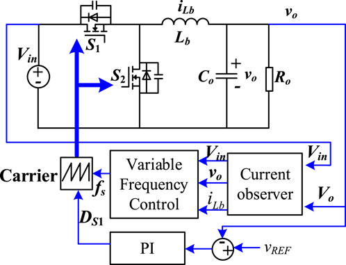
FIGURE 7. Control block diagram of the proposed method.
To prove the availability and practicability of the proposed method, a simulation model and experimental prototype with 30 V–60 V input voltage, 24 V output voltage, and 75 kHz–150 kHz switching frequency is established, as shown in Figure 8A. The parameter design process is shown in Figure 8B. First, the basic circuit parameters, such as Pt, Vo, Vin range, and fS range, need to be determined. Then, based on the ZVS condition, the filter inductance value can be determined. Furthermore, based on the output voltage ripple coefficient, the output capacitance can be determined. Finally, the observer coefficients can be calculated. The specific parameters are shown in Table 1.
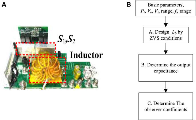
FIGURE 8. Experimental prototype and design process. (A) Photograph of the prototype. (B) Parameter design process.
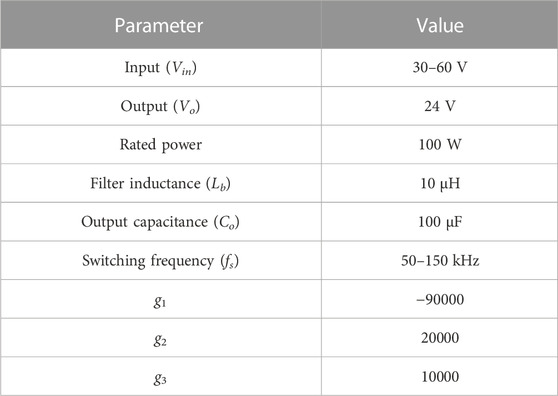
TABLE 1. Specific parameters.
A comparison of the simulation waveforms of fixed frequency control and the proposed control strategy is shown in Figure 9. It follows that the designed current observer can accurately estimate the average inductance current during load switching. Under traditional fixed switching frequency control, the filter inductor current average value increases as the load increases. Due to the fixed switching frequency, the inductor current ripple is also constant. When the minimum value of the filter inductor current is greater than zero, the converter will operate in a hard switching state, so the switching loss increases and the conversion efficiency decreases. Under the proposed CRM control, the switching frequency will be adaptively modified in accordance with the operating conditions, ensuring the implementation of ZVS soft switching and achieving the lowest current ripple.
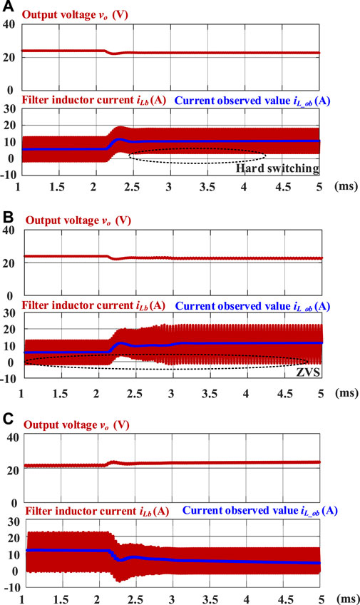
FIGURE 9. Comparison of simulation waveforms. (A) Fixed frequency control. (B) Proposed CRM control (half load to full load). (C) Proposed CRM control (full load to half load).
The steady-state experimental waveforms under half- and full-load are depicted in Figure 10. When the input voltage changes, the duty cycle will change accordingly to control the constant output voltage. In addition, under the proposed CRM control, when the load and working voltage change, the switching frequency will be adaptively adjusted, which is the basis of the implementation of ZVS and optimization of the current ripple. Because S2 is the synchronous rectifier MOSFET and can certainly achieve ZVS, only the ZVS waveforms of S1 are shown. These waveforms set forth the important fact that the drain-source voltage of MOSFET has been decreased to zero before it is turned on. According to the ZVS analysis, ZVS is difficult to achieve under full load and easy to achieve under light load. Therefore, according to the experimental results, we can conclude that the proposed control method can achieve full-range ZVS.
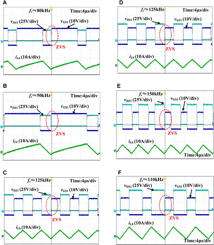
FIGURE 10. Steady-state waveforms. (A) Input 30 V, half load. (B) Input 30 V, full load. (C) Input 48 V, half load. (D) Input 48 V, full load. (E) Input 60 V, half load. (F) Input 60 V, full load.
The load-changing dynamic experimental waveforms are shown in Figures 11A, B. If the load steps from full to half load, the switching frequency increases rapidly to achieve ZVS and minimize the current ripple. Similarly, if the load steps from half to full load, the switching frequency decreases rapidly and soft switching is always ensured. The dynamic experimental waveforms of input voltage change are displayed in Figures 11C, D. When the input voltage changes, the output voltage can always be clamped at 24 V. Therefore, under the proposed CRM control, the bidirectional buck/boost converter has good dynamic performance. The experimental results demonstrated the proposed CRM control to be effective.
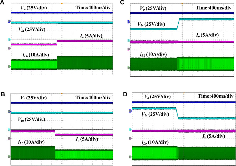
FIGURE 11. Dynamic waveforms. (A) Half to full load. (B) Full to half load. (C) 30 V–60 V. (D) 60 V–30 V.
The measurement efficiency comparison between the traditional fixed frequency (FF) control and the proposed CRM control is shown in Figure 12. Under the fixed frequency control, the switching frequency is always equal to 100 kHz. It can be seen that under the same operating conditions, the conversion efficiency of the proposed CRM control strategy is higher than that of the traditional fixed frequency control.
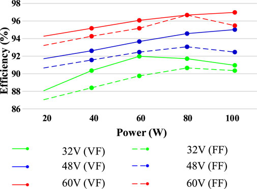
FIGURE 12. Measurement efficiency curve.
A current observer-based digital critical conduction mode control of a bidirectional DC–DC converter with full-range soft switching is explored in this paper. The bidirectional DC/DC converter works in the CRM mode, and full-range ZVS and optimal current ripple can be achieved. The proposed CRM control is achieved by the designed current observer without any ZCD circuit or current sensors. In addition, the proposed current observer can estimate the inductor current over a wide range of load and voltage variations. Therefore, the proposed control method can be applied to a wide range of charging and discharging applications. Finally, a prototype is built, and the simulation and experimental results prove the correctness and advantages of the proposed method.
The original contributions presented in the study are included in the article/Supplementary Material; further inquiries can be directed to the corresponding author.
All authors listed have made a substantial, direct, and intellectual contribution to the work and approved it for publication.
This work was financially supported by the Science and Technology Project of State Grid Hunan Electric Power Company Limited (5216A5220003).
Authors DW and LL were employed by the company Country State Grid Hunan Electric Power Company Limited Research Institute.
The authors declare that this study received funding from State Grid Hunan Electric Power Company Limited. The funder had the following involvement in the study: study design, collection, analysis, interpretation of data.
The remaining authors declare that the research was conducted in the absence of any commercial or financial relationships that could be construed as a potential conflict of interest.
All claims expressed in this article are solely those of the authors and do not necessarily represent those of their affiliated organizations, or those of the publisher, the editors, and the reviewers. Any product that may be evaluated in this article, or claim that may be made by its manufacturer, is not guaranteed or endorsed by the publisher.
Baek, J., Choi, W., and Cho, B. (2013). Digital adaptive frequency modulation for bidirectional DC–DC converter. IEEE Trans. Ind. Electron. 60, 5167–5176. doi:10.1109/TIE.2012.2224075
Basharat, S., Awan, S. E., Akhtar, R., Hussain, A., Iqbal, S., Shah, S. A., et al. (2021). A duty cycle controlled ZVS buck converter with voltage doubler type auxiliary circuit. Front. Energy Res. 9. doi:10.3389/fenrg.2021.550115
Cai, Jiahui, Zhao, Lei, Wei, Chuliang, and Liang, Jiawei (2022). Analysis of novel phase-shifted full-bridge converters with wide ZVS range reduced filter requirement. IEICE Electron. Express 19, 20210391. doi:10.1587/elex.18.20210391
Chen, X., Xu, G., Han, H., Sun, Y., and Su, M. (2022). Dual-mode bidirectional LLC-DAB converter based on a modulated coupled inductor. IEEE Trans. Power Electron. 38, 90–95. doi:10.1109/TPEL.2022.3204529
Chuang, Y.-C. (2010). High-efficiency ZVS buck converter for rechargeable batteries. IEEE Trans. Ind. Electron. doi:10.1109/TIE.2009.2035459
Chuang, Y.-C., and Ke, Y.-L. (2008). High-efficiency and low-stress ZVT-PWM DCto-DC converter for battery charger. IEEE Trans. Ind. Electron. 55, 3030–3037. doi:10.1109/TIE.2008.921218
Deng, W., Zhang, B., and Hu, Z. (2004). “Analysis of a novel boundary conduction mode (BCM) and voltage control of buck capacitor in single-stage PFC circuit,” in Proc. IEEE IPEMC, Xi 'an, China, August 14-1 6, 2004.
Fang, Z., Yang, R., Han, K., Cai, X., Hong, B., and Liu, L. (2023). Start-up and shut-down strategies of DR-based hybrid DC converter for offshore wind power transmission system. Front. Energy Res. 11. doi:10.3389/fenrg.2023.1091447
Hajiheidari, M., Farzanehfard, H., and Esteki, M. (2021). Asymmetric ZVS buck converters with high-step-down conversion ratio. IEEE Trans. Ind. Electron. 68, 7957–7964. doi:10.1109/TIE.2020.3013538
Hu, Jiajun, Chen, Houpeng, Xi, Li, Wang, Qian, Jin, Rong, Zhang, Yiyun, et al. (2014). A novel auxiliary-free zero inductor current detection scheme for step down non-isolated LED driver. IEICE Electron. Express 11, 20141011. doi:10.1587/elex.11.20141011
Ji, Weigui, Ran, Feng, Yuan, Ji, Lu, Xi, and Guo, Aiying (2017). A low cost battery equalizing scheme with buck-boost and series LC converter using synchronous phase-shift controller. IEICE Electron. Express 14, 20161166. doi:10.1587/elex.13.20161166
Lai, J. S., and Chen, D. (1993). “Design consideration for power factor correction boost converter operating at the boundary of continuous conduction mode and discontinuous conduction mode,” in Proc. IEEE APEC, San Diego, CA, USA, March 1993.
Lan, Z., Wu, F., He, D., Yu, X., Zeng, J., and Xiao, F. (2022). A high power quality buck-H auxiliary power converter in railway applications. Front. Energy Res. 10, 2022. doi:10.3389/fenrg.2022.926707
Lee, S.-S. (2014). Step-Down converter with efficient ZVS operation with load variation. IEEE Trans. Ind. Electron. 61, 591–597. doi:10.1109/TIE.2013.2247015
Li, N., Li, Z., Cao, Y., Wei, D., Xiao, Z., and Zhang, Y. (2023). Current stress optimization control strategy of the buck topology with the variable frequency/amplitude mode. Front. Energy Res. 10. doi:10.3389/fenrg.2022.1087775
Liu, Y.-C., Syu, Y. -L., Dung, N. A., Chen, C., Chen, K. -D., and Kim, K. A. (2020). High-switching-frequency TCM digital control for bidirectional-interleaved buck converters without phase error for battery charging. IEEE J. Emerg. Sel. Top. Power Electron. 8, 2111–2123. doi:10.1109/JESTPE.2019.2954602
Lu, Z., Xu, G., Xiong, W., Sun, Y., and Su, M. (2022). A quasi-two-stage isolated bidirectional buck-DAB converter for wide input voltage range. IEEE Trans. Power Electron 38, 1384–1390. doi:10.1109/TPEL.2022.3208105
Madhana, R., and Mani, G. (2022). Design and analysis of the multi-port converter based power enhancement for an integrated power generation system using predictive energy amendment algorithm. Front. Energy Res. 10. doi:10.3389/fenrg.2022.1000242
Marxgut, C., Krismer, F., Bortis, D., and Kolar, J. W. (2014). Ultraflat interleaved triangular current mode (TCM) single-phase PFC rectifier. IEEE Trans. Power Electron. 29, 873–882. doi:10.1109/TPEL.2013.2258941
Mohammadi, M. R. (2020). An active-clamping ZVS interleaved buck/boost Bi-directional converter with one auxiliary switch. IEEE Trans. Ind. Electron. 67, 7430–7438. doi:10.1109/TIE.2019.2945284
Pattnaik, S., Panda, A. K., and Mahapatra, K. (2010). Efficiency improvement of synchronous buck converter by passive auxiliary circuit. IEEE Trans. Ind. Electron. 46, 2511–2517. doi:10.1109/TIA.2010.2070831
Premkumar, M., Kumar, C., and Sowmya, R. (2019). Analysis and implementation of high-performance DC-DC step-up converter for multilevel boost structure. Front. Energy Res. 7. doi:10.3389/fenrg.2019.00149
Ren, X., Zhou, Y., Guo, Z., Wu, Y., Zhang, Z., and Chen, Q. (2020). Simple analog-based accurate variable on-time control for critical conduction mode boost power factor correction converters. IEEE J. Emerg. Sel. Top. Power Electron. 8, 4025–4036. doi:10.1109/JESTPE.2019.2926794
Reusch, D., and Strydom, J. (2015). Evaluation of gallium nitride transistors in high frequency resonant and soft-switching DC–DC converters. IEEE Trans. Power Electron. 30, 5151–5158. doi:10.1109/TPEL.2014.2364799
Rodrigues, J. P., Mussa, S. A., Heldwein, M. L., and Perin, A. J. (2009). Three-level ZVS active clamping PWM for the DC–DC buck converter. IEEE Trans. Power Electron. 24, 2249–2258. doi:10.1109/TPEL.2009.2022535
Sable, D. M., Lee, F. C., and Cho, B. H. (1992). “A zero-voltage-switching bidirectional battery charger/discharger for the NASA EOS satellite,” in Proc. IEEE APEC, Boston, MA, United States, February 1992.
Samad, M. A., Xia, Y., Manzoor, T., Mehmood, K., Saleem, A., Milyani, A. H., et al. (2023). Composite model predictive control for the boost converter and two-phase interleaved boost converter. Front. Energy Res. 10. doi:10.3389/fenrg.2022.1009812
Sha, D., Zhao, Y., and Zhang, D. (2022). ZVS-interleaved synchronous buck DC–DC converter with a coupled inductor by varying switching frequency and deadtime. IEEE Trans. Power Electron. 37, 8190–8198. doi:10.1109/TPEL.2022.3141253
Tao, P., Cui, Y., and Liang, J. (2021). Research on efficient soft switching based on MPPT of PV power generation system. Front. Energy Res. 9. doi:10.3389/fenrg.2021.728789
Keywords: bidirectional DC–DC converter, ZVS, critical conduction mode, current observer, soft switch
Citation: Wan D, Li J, Zhang L and Xu J (2023) Current observer-based critical conduction mode control of a bidirectional DC–DC converter in battery charging/discharging applications. Front. Energy Res. 11:1241718. doi: 10.3389/fenrg.2023.1241718
Received: 17 June 2023; Accepted: 14 July 2023;
Published: 03 August 2023.
Edited by:
Tao Xu, Shandong University, ChinaReviewed by:
Zhiqiang Guo, Beijing Institute of Technology, ChinaCopyright © 2023 Wan, Li, Zhang and Xu. This is an open-access article distributed under the terms of the Creative Commons Attribution License (CC BY). The use, distribution or reproduction in other forums is permitted, provided the original author(s) and the copyright owner(s) are credited and that the original publication in this journal is cited, in accordance with accepted academic practice. No use, distribution or reproduction is permitted which does not comply with these terms.
*Correspondence: Jingtao Xu, eGp0NHVnb0Bjc3UuZWR1LmNu
Disclaimer: All claims expressed in this article are solely those of the authors and do not necessarily represent those of their affiliated organizations, or those of the publisher, the editors and the reviewers. Any product that may be evaluated in this article or claim that may be made by its manufacturer is not guaranteed or endorsed by the publisher.
Research integrity at Frontiers
Learn more about the work of our research integrity team to safeguard the quality of each article we publish.