 Cheng Guo
 Ziyue Xin
- National Key Laboratory for Electromagnetic Energy, Naval University of Engineering, Wuhan, China
In the voltage source power electronic converter, DC-link capacitors usually work as buffering elements between the DC and AC sides. The high failure rate and large space occupied by the DC-link capacitors directly affect the reliability and power density of the converters. The analysis and calculation of the DC-link capacitor current is crucial to achieve the refined design of converters. In this work, the analysis and calculation methods of DC-link capacitor current are divided into three categories, according to the calculation principle, namely, simulation method, RMS analysis method, and spectral analysis method, and their calculation methods are summarized. First, the types of capacitors and their characteristics are briefly introduced. Second, the three-phase two-level converter is taken as an example to introduce the basic principles, calculation steps, application scope, advantages, and disadvantages of the latter two methods in detail, as well as the influence of non-ideal factors, such as the output ripple on the calculation results. This work also discusses the calculation of the multi-level converter’s DC-link capacitor current spectrum and the current characteristics of multi-phase converters, which are rarely reported. Third, the problem of resonance between the DC-link capacitors and the DC bus inductor is introduced. For the distributed arrangement of multiple DC-link capacitors on DC bus converters, this study proposes a method based on a constant current source equivalent circuit, which can accurately calculate the DC-link capacitor current spectrum that is affected by loop current and resonance. Finally, the current problems and future directions of the DC-link capacitor design are pointed out.
1 Introduction
With the continuous development of power electronics, the voltage source converter (VSC) is widely used in photovoltaic systems, wind power generation, motor drives, DC microgrids, and so on (Rixin et al., 2008; Yang et al., 2010; Colak et al., 2011; Kumar and Jain, 2014; Watanabe et al., 2016). Since pulse-width modulation (PWM) is usually used on the converter side of the VSC, high frequency harmonics are introduced on the DC side (Dahono et al., 1996; Cross et al., 1999; Kolar and Round, 2006). The DC side usually uses DC-link capacitors as a buffer and voltage regulator, and several typical configurations are shown in Figure 1 (Wang and Blaabjerg, 2014). The main roles of DC-link capacitors include 1) compensating the power pulsation on the AC side and buffering the energy exchange between the AC and DC sides; 2) stabilizing the DC-side voltage and suppressing the voltage harmonics on the DC side; 3) absorbing the current ripple on the DC bus; 4) providing transient power peaks to the load; and 5) absorbing the demagnetization energy of the drive motor in case of an emergency shutdown of the converter (Kolar and Round, 2006; Wang and Blaabjerg, 2014). It can be said that the DC-link capacitors are the most important component observed on the DC side but also one of the components with the highest failure rate in the power electronic systems (Yang et al., 2011; Wang et al., 2013; Wang and Blaabjerg, 2014). The operating conditions of DC-link capacitors (temperature, humidity, ripple current, and voltage) significantly affect their reliability, and their lifetime estimation has been a hot topic of research (Gasperi, 1996; Gasperi, 2005; Yang et al., 2018; Torki et al., 2023). The literature (Kolar and Round, 2006) states that the operating voltage and especially the operating temperature have a significant effect on the operating life of electrolytic capacitors: the failure rate of an aluminum electrolytic capacitor is reduced to 60% if it operates at 0.9 times of its rated voltage compared to when it operates at the rated voltage; if the operating temperature is reduced, the expected life doubles for every 10°C reduction relative to the rated temperature. The literature (Wang et al., 2018) considers the non-linear process of equivalent series resistance (ESR) growth and capacitance reduction during degradation, and then a non-linear accumulated damage model is proposed to achieve the long-term evaluation of the capacitor life under variable loading conditions. The literature (Delmonte et al., 2020) proposes a procedure based on finite element simulations to compute a thermal model of capacitors, coupling with electrical SPICE simulations to evaluate the maximum operative temperature of capacitors. This method can reduce the damage caused by the overheating of capacitors and increase their service life in practical applications. Therefore, many methods have been proposed by domestic and foreign scholars to reduce the DC-side pulsation and heating of the capacitors, such as the optimization of the structure layout and application of new modulation methods to extend the life of DC-link capacitors (Kieferndorf et al., 2004; Su and Tang, 2012; Basler et al., 2015; Diana et al., 2015; Diana et al., 2018; Nie and Schofield, 2019; Yan et al., 2019). In addition, considering that the DC-link capacitors are components that occupy the largest space in a converter system (Huiqing et al., 2012; Ko et al., 2018), in order to improve the converter power density and prevent an increase in system cost, volume, and weight due to overdesigning, the design margin of the DC-link capacitors should be as small as possible while ensuring reliability, which requires a more accurate estimation of the thermal stress of the DC-link capacitors.
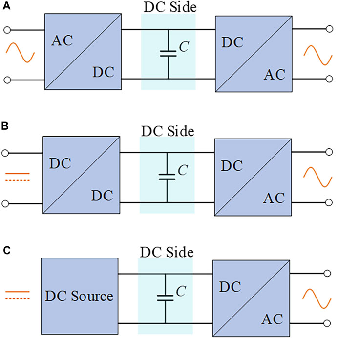
FIGURE 1. Typical configurations of power electronic conversion systems with DC-link capacitors; (A) AC-DC-AC converter, (B) DC-DC-AC converter, and (C) DC-AC converter for the DC power supply.
The heating of DC-link capacitors is mainly caused by the current flowing through the capacitors and their own ESR (McGrath and Holmes, 2009; Wang and Blaabjerg, 2014). The ESR is an inherent property of the capacitor, so the analysis and calculation of the DC-link capacitor current is the basis of the capacitor design and life prediction, which is an important design to ensure the reliability of the converter. Therefore, the analysis and calculation of the DC-link capacitor current is worthy of an in-depth study in order to meet the minimum fault interval requirement of the converter and also realize the refined design of the system and improve the power density. The existing DC-link capacitor current analysis methods can be divided into three main types as shown in the following sections.
1.1 Simulation method
Simulation can accurately obtain the current waveform flowing through the DC-link capacitors, but in addition to the time required to build the simulation model, each simulation can only solve a set of parameters. Besides, it is difficult to figure out the influence that each parameter has on the capacitor current, and it is impossible to establish the functional relationship between the operating point of the converter (determined by the modulation index, amplitude, and phase of the output voltage and current) and capacitor current. The guidance for a practical engineering design is limited.
1.2 Root mean square analysis method
The analytical method generally calculates the RMS of the DC-link capacitor current in the time domain. This method calculates the RMS value of the converter input current by analyzing the mean value and RMS value of the carrier wave period of the converter input current and using the integral in the time domain. When the output ripple on the rectifier side is not considered, the RMS value of the DC-link capacitor current becomes equal to the RMS value of the input current of the converter minus its average value. This method usually ignores the converter output current ripple but still maintains high accuracy and is the most used analysis method nowadays.
1.3 Spectral resolution method
The ESR of capacitors is sensitive to frequency and temperature, and failure to consider the effects of temperature, voltage, and frequency on the ESR will result in prediction errors (Wang and Blaabjerg, 2014); in order to calculate the heating of DC-link capacitors more accurately, it is sometimes necessary to calculate the spectrum of the capacitor current. The double Fourier analysis is the basis for calculating the DC-link capacitor current spectrum. This method is more complex than that of calculating current RMS values, but after obtaining the capacitor current spectrum (harmonic resolution), the frequency and temperature can be taken into account in the temperature calculations of the capacitors according to the ESR model of the capacitors and thermal stress can be estimated more accurately.
This article will first introduce the types and characteristics of DC-link capacitors, and then introduce the RMS analysis method and the spectral analysis method in detail. The common characteristics of the DC-side DC-link capacitor current with each parameter will be analyzed by using the RMS analysis method, and the effects of the output current ripple and diode reverse recovery on the DC-link capacitor current will be introduced. The harmonic analysis method is then introduced, and the rarely reported calculation method of the DC-link capacitor current for multi-level converters and the characteristics of capacitor current for multi-phase converters are further discussed. Meanwhile, considering the rapid development of new energy industries and wide application of advanced motor drive systems, converters with a distributed arrangement of multi-phase or multiple DC-link capacitors have been gradually adopted. In this arrangement, multiple DC-link capacitors may resonate with the DC bus spurious parameters, which greatly affect the accurate calculation results of the DC-link capacitor current. In this work, a method to analyze the resonance characteristics of distributed multi-capacitor systems is proposed, and a method to analyze and calculate the spectrum of distributed DC-link capacitor current, considering the effect of resonance, is proposed. Finally, an outlook on the method of DC-link capacitor current analysis and calculation is given.
2 DC-link capacitors
Capacitors that are used as DC-link capacitors are usually of three types, namely, aluminum electrolytic capacitors, metallic polypropylene film capacitors, and ceramic capacitors (Williams, 1986; Wang and Blaabjerg, 2014). Each one of these three types of capacitors has its own characteristics and is suitable for different applications. Aluminum electrolytic capacitors have the highest energy density and lowest energy loss but have relatively large ESR and wear problems due to electrolyte evaporation (Gasperi, 2005). Metallic polypropylene film capacitors use plastic films as dielectric material and have good AC characteristics with small size, wide frequency range, and operating temperatures up to 200°C but are relatively expensive and suitable for high current ripple applications (Huiqing et al., 2012). Ceramic capacitors are suitable in high-power and high-frequency switching power supplies with small size, low cost, and more balanced performance. In general engineering applications, converter systems for driving motors mostly use aluminum electrolytic capacitors (Huiqing et al., 2012).
The equivalent circuit model of the capacitor is shown in Figure 2, where CR is the capacitance; RS is the series equivalent resistance ESR determined by the lead and junction resistance; LS is the series equivalent series inductance (ESL) caused by the structure and supply line, which can be neglected at lower frequencies. Ri is the insulation resistance, which is usually large; Rd is the dielectric loss equivalent resistance caused by dielectric absorption and molecular polarization; and Cd is the inherent dielectric absorption capacitance, both of which usually need to be considered only in electrolytic capacitors operating at high frequencies.
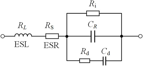
FIGURE 2. Simplified lumped model of capacitors.
The equivalent circuit parameters of the capacitor vary with the operating temperature, voltage stress, and frequency, as shown in Figure 3 (Williams, 1986). Failure to consider these variations will lead to incorrect calculations of electrical and thermal stresses in the capacitor and affect the accuracy of reliability estimation. Therefore, the accuracy of life estimation based on the harmonic spectrum of the current flowing through DC-link capacitors is higher during the refinement of the DC-link capacitor design.
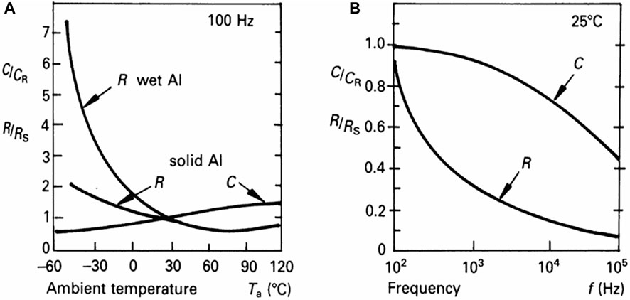
FIGURE 3. Variation of capacitor equivalent circuit parameters with frequency and temperature for 47 μF and 350 V electrolytic capacitor, respectively (Williams, 1986). (A) Variation of capacitor equivalent circuit parameters with temperature, (B) Variation of capacitor equivalent circuit parameters with frequency.
2.1 Calculating RMS value of DC-link capacitor current
Calculating the capacitor current RMS value is a relatively quick and intuitive method, in which the calculation process is easy to understand, the physical meaning is clearer, and it is widely used in applications that do not require high accuracy in estimating capacitor heating (Kolar and Round, 2006; Kai et al., 2016). The following is an example of the most common three-phase two-level converter to introduce its calculation process.
The main circuit of the three-phase two-level converter is shown in Figure 4. The converter side uses space vector modulation (SVM) with two levels per phase bridge arm and 23 = 8 states in total for the three phases. The reference voltage vector
where Vref is the reference voltage amplitude, ω is the rotational angular velocity, and the modulated carrier wave period is Ts.
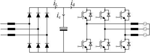
FIGURE 4. Main circuit of three-phase two-level converter.
When the reference vector is in sector 1, in order to minimize the number of switch actions, the vector synthesis in one carrier wave period is
where
The upper and lower switching signals of the bridge arm on the converter side are complementary. From the circuit in Figure 4, it can be seen that the input current id on the converter side is determined by the AC load current together with the switching state of the three-phase switching tubes. Using the switching function to express the state of the switching tube, the switching function is 1 or 0, where 1 means the switching tube is turned on and 0 means it is turned off, and at this time, the expression of the converter side DC bus input current id is
where Sx1 (x = a, b, c) are the switching functions of the tubes on the three-phase bridge arm; ix is the AC output current of the three-phase converter bridge.
Since converters usually carry inductive loads such as motors, their output current ripple is relatively small, and the ripple can usually be neglected and treated as a standard sinusoidal waveform. The literature (Kolar and Round, 2006) explored the effects of ignoring/not ignoring the output current ripple on the solution results and pointed out that the difference between the calculated results of the DC-link capacitor current does not exceed 8%. For a three-phase balanced load, in neglecting the load current ripple, the load current satisfies Eq. 6:
where Io is the RMS value of the load current. According to the aforementioned analysis, the average value of the input current on the converter side over half a carrier wave period is
In Eqs 3, 4,
Further simplifying it to
where M = 2Vref/Vdc. For a three-phase balanced load, the average value of the input current on the converter side of its converter is a constant over half a carrier wave period, which is only related to the modulation index and load and is independent of the carrier wave frequency. From the harmonics point of view, id contains no lower harmonic component except for the DC component and the carrier harmonic component.
The RMS value of id within half a carrier wave period satisfies
Due to the symmetry of the three-phase converter, the RMS value of the id over the fundamental period is obtained by integrating over a sector (π/3):
and solving to get
According to the circuit shown in Figure 4, the converter-side input current id, the DC-link capacitor current ic, and the rectifier-side output current iL are satisfied with the following:
When the ripple of the rectifier output current is not considered, iL contains only the DC component, whose magnitude is the same as the DC component Id,avg of the input current on the converter side. According to Parseval's theorem, the RMS value of the DC-link capacitor current at this time satisfies the following:
By substituting Eqs 10, 13 into Eq. 15 we obtain
When considering the current ripple obtained by the rectifier side, the input current id on the converter side and output current iL on the rectifier side can be expressed as follows:
where id,ac is the AC component of the input current on the converter side, IL,avg is the DC component of the output current on the rectifier side, and iL,ac is its AC component. Equation 14 can be simplified as follows:
The relationship between the frequency and phase of each harmonic of id,ac and iL,ac will affect the RMS value of ic. According to the Cauchy–Schwarz inequality, the RMS value of the aforementioned equation satisfies the relationship.
Equation 20 represents the worst-case maximum RMS value of the DC-link capacitor current.
2.1.1 Analysis of calculation results
According to Eq. 16, the RMS value of the DC-link capacitor current can be considered a function related to the load current and modulation index. When cosφ is close to 1, Ic,rms is maximum when
According to Eq. 10, id has no DC component when cosφ is close to 0. The DC-link capacitor current Ic,rms in Eq. 16 increases with the modulation index M. The ratio of its effective value to the load current (Ic,rms/Io) is approximately proportional to
When the modulation index M is close to
cosφ in Eq. 16 is approximately dropped, and the value of Ic,rms is largely independent of φ.
Figure 5 shows the relationship between the ratio of the RMS values of the DC-link capacitor current and load current (Ic,rms/Io) with each parameter. As can be seen in Figure 5A, Ic,rms/Io approaches its peak (extreme value) when M is close to 0.6; and when cosφ = 0, Ic,rms/Io no longer exhibits the extreme value characteristic but increases monotonically with M, and it is approximately proportional to
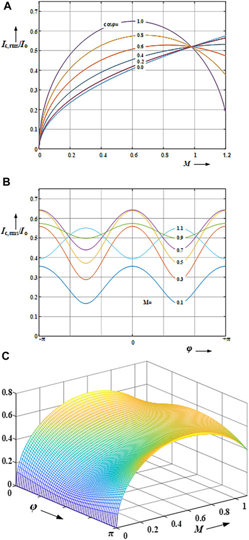
FIGURE 5. Effect of each parameter on DC-link capacitor current (Kolar and Round, 2006). (A) Effect of M on DC-link capacitor current; (B) effect of φ on DC-link capacitor current; and (C) three-dimensional representation.
The aforementioned analysis of the relationship between the DC-link capacitor current and variables is for the three-phase two-level converter topology, but the laws and trends of this relationship are also applicable to other conventional multi-phase and multi-level converter structures, where only the ratio and amplitude of the parameters between the corresponding variables are different. The correctness of the calculation results can initially be judged according to the corresponding trends in practical engineering.
2.1.2 Development of current RMS calculation
On the basis of the aforementioned calculation methods, domestic and foreign scholars have also optimized many of these and expanded new application areas. The literature (Pei et al., 2015; Li and Jiang, 2018) provides a more accurate analytical solution for the RMS value of the DC-link capacitor current, considering the ripple of the load current, and showing the calculation result that the load current ripple will increase the peak DC current, but its expression involves several AC side parameters and the result is more complicated. In the literature (Welchko, 2007), the RMS value of the DC-link capacitor current of a three-phase two-level converter after eliminating the common-mode voltage is calculated by analyzing the vector synthesis method, and the results show that the elimination of the common-mode voltage leads to an increase in the DC-link capacitor current to 1.3–2 times that of the original one. In the literature (Guo et al., 2018), the converter shunt diode reverse recovery problem was considered and the method for solving the RMS value of the DC-link capacitor current was optimized by considering more factors that affect the calculation results, such as the switching frequency of the converter, reverse recovery time, and current of the inverse shunt diode.
It should be noted that no matter how accurately the RMS value of the DC-link capacitor current is calculated, the method has its unavoidable limitation that the amplitude of each harmonic of the capacitor current is not available. This will seriously affect the accuracy of the results when calculating the capacitor heating, and the error will exceed the impact of the output current ripple, diode reverse recovery time, and other factors on the heating calculation.
2.2 Calculation of DC-link capacitor current spectrum
Considering that the equivalent circuit parameters of capacitors are related to the operating temperature, voltage stress, and frequency, in order to estimate and calculate electrical and thermal stresses of capacitors more accurately, the current harmonic spectrum flowing through the DC-link capacitors has to be calculated for a more accurate estimation of heat generation in engineering. The current ripple on the DC side of the converter is observed as being caused by the PWM modulation strategy, and the current analysis of the PWM strategy mainly uses the double-Fourier analysis (Holmes, 1998; Moynihan et al., 1998; McGrath and Holmes, 2002).
2.2.1 Double-Fourier analysis
By continuing to use the three-phase two-level converter shown in Figure 4 as an example, the process of calculating the harmonic expression for the DC-link capacitor current using the double-Fourier analysis is described. Assuming a SPWM strategy at the converter side, we set the time variable as follows:
where
where
To simplify the expression, the modulated signal is expressed in the cosine form:
where
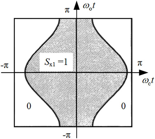
FIGURE 6. Unit cell of Sa1 switching function.
The boundary of the unit cell shown in Figure 6 specifies the range of integration defined in Eq. 25, and it is only in this range that the switching function Sa1 = 1 and Eq. 25 are rewritten as
We solve the equation
and since the carrier phase angle is the same for all three half-bridge arms at any moment, for the convenience of calculation, the carrier phase angle
Assuming that the converter output current is a three-phase symmetric sine wave, for the convenience of calculation, Eq. 6 is expressed in the cosine form, and Eqs 6, 28 are taken into Eq. 5 to obtain the harmonic expression for the input current id on the converter side as follows:
The aforementioned equation can be reduced to a convolution integral in the frequency domain (McGrath and Holmes, 2009) or solved directly by using the prosthaphaeresis, and the result is
where
The purpose of using the cosine form to express the modulating signal and output current on the converter side of the converter is to simplify the double-Fourier integral equation; except for the initial phase difference of π/2 of the modulating waveform, the connotations of using the sine and cosine forms are exactly equivalent. When using the sine form expression in Eq. 6, the solution results will not be any different, except that Eqs 24, 31 will be slightly more complicated.
According to Eq. 1, the DC-link capacitor current ic is equal to the DC-side input current id minus the rectifier-side output current iL. When the rectifier-side current ripple is not considered, ic is equal to id, excluding its DC component.
The spectrum of the DC-link capacitor current is obtained by Eq. 33.
With Id_h,rms(k) denoting the RMS value of the k-th harmonic of the input current on the converter side, the RMS value of the current flowing through the DC-link capacitors according to Parseval's theorem is
2.2.2 Considering AC output ripple
When considering the converter output current ripple, a correction to Eq. 30 is required. Usually, the corresponding harmonic component is superimposed on the fundamental component of the output current. According to the literature (Renken, 2005), the current ripple can be considered to be a result of the action of the converter output voltage on the filter circuit, and the output port load is equated to the circuit shown in Figure 7, where ix,f is the fundamental component of the output current and the remaining components of each ripple are equal to the output voltage harmonics divided by the corresponding filter circuit impedance. Assuming that the converter output voltage harmonics resolution is
where
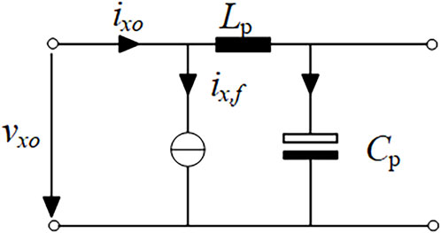
FIGURE 7. Equivalent circuit of converter load.
After the output current expression is corrected, it can then be substituted into Eqs 30–34 to calculate the DC-link capacitor current spectrum. In general, the output current ripple causes the DC-link capacitor current to become large when the output power is small. However, when the output power increases, the DC-link capacitor current caused by the fundamental component of the output current dominates, and the effect produced by the output ripple is very small and can basically be ignored.
3 Calculation of the multi-level, multi-phase converter structure DC-link capacitor current
3.1 Multi-level converter
In medium and high voltage and high-power applications, with the increase in DC-side voltage, the conventional two-level converters can no longer meet the requirements of the device withstand voltage levels. Multi-level converters are widely used in medium voltage and high-power applications because of the advantage of withstanding high voltage levels, no requirement for series connection of power devices, low harmonic distortion, and low switching losses. The conventional multi-level topologies mainly include neutral point clamped (NPC) (Nabae et al., 1981; Jayakumar et al., 2021; Xin et al., 2022), flying capacitor (FC) (Defay et al., 2010; Barth et al., 2019; Ye et al., 2021), and cascaded H-bridge (CHB) converters (Hammond, 1997; Lezana et al., 2008; Mhiesan et al., 2020; Maheswari et al., 2021), whose topologies are shown in Figure 8, where Figure 8A shows the topology of the three-level neutral point clamped (3L-NPC), Figure 8B shows the topology of three-level flying-capacitor (3L-FC), and Figure 8C shows the topology of the five-level cascaded H-bridge (5L-CHB).

FIGURE 8. Multi-level converter phase-leg topologies; (A) 3L-NPC, (B) 3L-FC, and (C) 5L-CHB.
The behavior of the switching device in the form of a switching function is continuously described, assuming that the dead time of the switch is not considered, and while treating the phase output current as a sinusoidal wave, the expression for the input current of the single bridge arm of the 3L-NPC converter is obtained according to Figure 8A.
For the 3L-FC converter of Figure 8B, the relationship between the input current and flying capacitor is
For the 5L-CHB converter shown in Figure 8C, its input current expression is
These results show that for all these converter topologies, the DC input current or suspended capacitor current of a single bridge arm is defined by the product of two time-varying signals. When the multi-phase bridge arms are combined into a complete converter system, the DC-side current is the superposition of the input currents of each phase bridge arm.
For the calculation of the spectrum of the switching function, the same double-Fourier transform approach can be used for multi-level converters: first, the unit cell of the switching function is calculated according to the modulation strategy, then the integration range is determined according to the unit cell, and finally the spectral expression of the switching function is calculated (McGrath and Holmes, 2002; Bierhoff and Fuchs, 2008; Orfanoudakis et al., 2013; Sun et al., 2014).
3.2 Multi-phase converter
In recent years, multi-phase motors have been widely used in various fields because of their small size, light weight, and high torque density (Levi et al., 2007); the accompanying multi-phase converter technology is developing rapidly and is widely used. Generally speaking, the converter side of a multi-phase converter is one containing a multi-phase converter bridge arm; its DC side only has a set of DC-link capacitors, which are arranged between the rectifier side and multi-phase converter side.
The input current of the multi-phase converter side can simply be regarded as the superposition of the input currents of the bridge arms of each phase. Regardless of the number of phases on the converter side, the input current is obtained by a simple calculation of the superposition theorem. Taking the literature as an example, which first calculates the analytic expressions of the input current spectrum of a single-phase two-level H-bridge converter, and then gives the expressions of the input current spectrum of a 3-phase and 12-phase H-bridge converter by linear superposition of the output currents of each phase H-bridge converter unit.
It is shown that the RMS of the DC-side current will become significantly smaller as the number of converter phases increases (Parsa, 2005; Levi, 2008), and the multi-phase converter structure can reduce the DC-link capacitor requirements. This is because some of the harmonics of the input currents of each phase at the multi-phase converter side cancel each other on the DC bus, and as the number of phases increases, only the harmonics of the n*phase times will remain, and the rest of the harmonics all cancel each other to zero.
Many modulation strategy optimization methods have also been proposed by domestic and foreign scholars to reduce the DC-side current stress in multi-phase converter structures. The literature (Kim and Sul, 1993; Kieferndorf et al., 2004; Su and Tang, 2012; Rouhana et al., 2014; Umesh and Sivakumar, 2017) investigated the method of reducing DC-link capacitor current in-depth by carrier phase shifting; based on this, the literature (Diana et al., 2019) studied the RMS value of the input current of a five-phase two-level converter and explored the effect of the interleaved phase shifting strategy on the DC-link capacitor current. It was found that a correct phase-shifting strategy can reduce the DC capacitor current by approximately 40%. Multi-phase converter systems bring more freedom to the modulation strategy (Su and Tang, 2012; Diana et al., 2015), and converters with a large number of phases can significantly reduce the magnitude of the DC-link capacitor current by a reasonable modulation strategy (e.g., carrier phase-shift modulation).
4 DC-link capacitor resonance problem
4.1 Resonance between DC-link capacitors and bus inductor
Generally speaking, the resonance of DC-link capacitors and bus inductor is relatively weak, and this resonance problem is usually ignored. In actual engineering, when the DC-side cable is very long and the line inductance is large, the line inductance will resonate with the DC-link capacitors and affect the current flow through the DC-link capacitors due to the presence of the input current ripple on the converter side. Foreign scholars have studied the resonance of DC-link capacitors of the three-phase two-level converter, and the literature (Mantzanas et al., 2019) points out that the resonance degree of the DC-link capacitors is affected by the PWM carrier wave frequency and the magnitude of the inherent resonance frequency of the circuit. When the ratio of the PWM carrier wave frequency to resonant frequency is denoted by Fres, and the ratio of the PWM carrier wave frequency toward the modulating wave frequency is denoted by Fac.
The quality factor Q of the DC-side circuit is equal to
where C is the DC-link capacitor, L is the DC bus inductor, Rdc is the DC supply resistance, Rc is the series resistance of the DC-link capacitors, fs is the carrier wave frequency, and fo is the modulating wave frequency.
The literature (Mantzanas et al., 2019) shows that when Fres > max (10, 10/Q) and Fac ≫ 10, the inherent resonant frequency of the circuit is very low, the carrier wave ratio is very high, and the resonance has very little effect on the DC-link capacitor current at this time, and the method introduced in Sections 3, 4 can accurately solve the current flowing through the DC-link capacitors.
When Fres < 1, the inherent resonant frequency of the circuit is higher than the carrier wave frequency, if there is no large enough damping in the resonant circuit composed of the DC-link capacitors and DC-side inductor (the quality factor Q is very high), then the resonance will be very strong and will seriously affect the size of the DC-link capacitor current. At this time, the calculation method in Sections 3, 4 will have a huge error.
Figure 9 shows the relationship between the error of the RMS value calculation method of the DC-link capacitor current and each resonance parameter mentioned in Section 3. When Fres is very small (Fres < 0.1) or Fres is large (Fres > 3), the error of the conventional RMS calculation results is small. The larger the quality factor Q, the larger the error caused in the calculation of the RMS value. This is because as Q gets larger, the resistance of the resonant circuit will be smaller and its resonance will become stronger, resulting in a significantly larger DC-link capacitor current, making the traditional RMS calculation results small and providing a negative relative error.
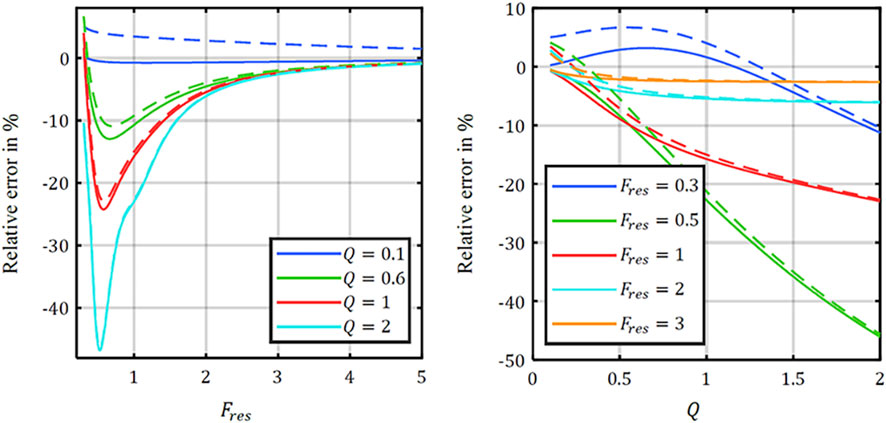
FIGURE 9. Relative error in RMS method of DC-link capacitor current (Mantzanas et al., 2019).
This work argues that this is essentially because when Fres is large, the carrier wave frequency of the converter is greater than the inherent resonant frequency of the circuit, and the resonant frequency is close to the fundamentals of the converter input current spectrum, and the amplitude of the harmonic components in the vicinity is close to zero, and the resonance does not have a large impact on the input current spectrum. When Fres is very small, the inherent resonant frequency of the resonant loop is high and falls outside the high carrier side band of the converter input current, and since the amplitude of these high harmonics is very small, they do not have a large impact on the input current spectrum. When 0.1 < Fres < 1, the resonant frequency falls within the low carrier side band of the converter input current, and the low carrier harmonic amplitude is large, which will significantly be amplified by the resonance, causing a significant increase in the DC-link capacitor current.
4.2 Resonance problem of multi-phase and multiple DC-link capacitors distributed arrangement structure
With the rapid development of new energy industry and the wide application of advanced transmission systems, some converter systems dealing in wind power generation, industrial transmission, vessel propulsion, and other fields gradually adopt the structure of the distributed arrangement of multi-phase DC-link capacitors based on the idea of a modular design. With this arrangement, multiple DC-link capacitors may generate more complex resonance with DC bus spurious parameters, forming a loop on the DC bus, which greatly affects the DC-link capacitor current.
In the field of vessel propulsion, new multi-phase open-winding propulsion motors are matched with multi-phase multi-level H-bridge converters. According to the DC 10 kV/tens of MW propulsion power demand, the converter side of the matched propulsion converter can adopt a five-phase H-bridge structure scheme based on four-level nested neutral point clamped (4L-NNPC) topology (Narimani et al., 2014; Tian et al., 2016; Tan et al., 2017), as shown in Figure 10.
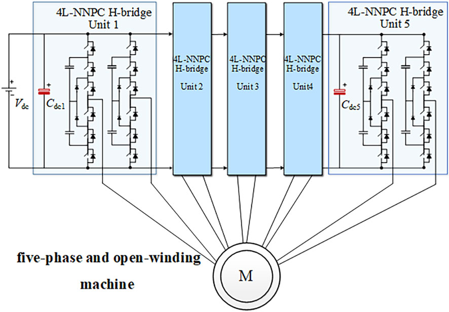
FIGURE 10. Main circuit of multi-phase converter motor system based on 4L-NNPC H-bridge topology.
This four-level five-phase H-bridge converter has a distributed arrangement of multiple DC-link capacitors, with independent DC-link capacitors on the DC side of each phase of the H-bridge power unit. Considering the effects of bus spurious parameters and DC-link capacitor series equivalent parameters, the topology of this type of multi-level five-phase H-bridge converter is shown in Figure 11.
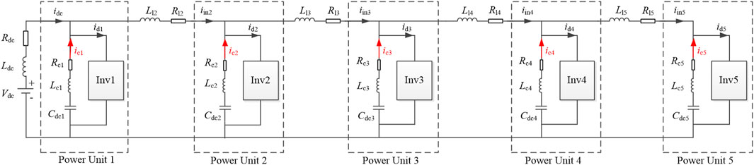
FIGURE 11. Main circuit of distributed capacitors of five-phase converter based on 4L-NNPC H-bridge topology.
Here, Invi denotes the phase i converter H-bridge power unit, ici denotes the current of the phase i DC-link capacitors; Rci and Lci are the phase i DC-link capacitor series equivalent resistance ESR and inductance ESL. Rli and Lli are the line resistance and inductance on the DC bus of section i, respectively. For the phase 1 power unit, its DC bus spurious parameters are combined into the DC power supply series impedance and are not listed separately. The five-phase power units in the actual converter have the same structure, the same length as the DC bus for each segment, and the same value for each phase parameter: Cdci = C, Rci = Rc, Lci = Lc, Rli = Rl, and Lli = Ll.
In order to simplify the resonant characteristics of the system, only the ripple introduced by the first phase H-bridge is considered first. The first phase H-bridge introduces the ripple current at both ends of the DC-link capacitor Cdc1 branch and equates it to a “constant current source” id1_ac, with the corresponding ripple output. The resonant equivalent circuit of the frequency conversion system is shown in Figure 12.
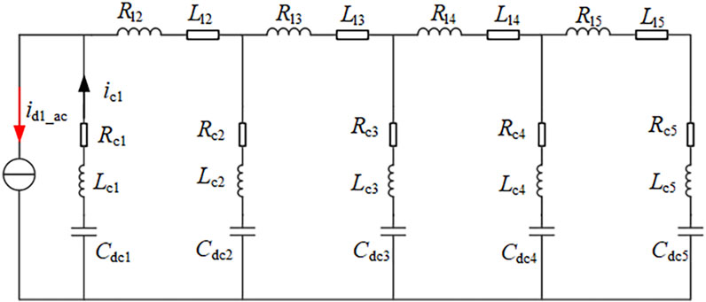
FIGURE 12. Equal circuit of common DC bus five-phase H-bridge converter, with the first phase ripple alone.
According to Kirchhoff laws, the magnitude of the current ic1 in the branch of the capacitor Cdc1 is
where Zeq is the equivalent line impedance after series–parallel connection of the rear four-phase DC-link capacitance and busbar spurious parameters.
where
When the resistance Rc and Rl are very small, the denominator of Zeq/(Zeq + Zc) tends to be 0 at certain angular frequencies, the circuit resonates, and there is a sharp increase in the amplitude of the current ic1 phenomenon. Formula (46) is more complex to develop and directly provides the results of the resonance point; when Rc and Rl tend to be 0, the resonance point can be expressed as
The resonant characteristics of the system equivalent circuit when the five-phase equivalent constant current sources act separately are similar to those mentioned above. The analysis shows that the DC-link capacitors may resonate with the DC bus inductor when the DC-link capacitors are arranged in a distributed arrangement and the DC bus resistance and the series resistance of the capacitor are very small. If the frequency of a certain ripple of the bus current is close to the system resonance point, it will cause a sharp increase of this ripple on the DC-link capacitors and significantly affect the current component of the DC-link capacitors. When the frequency of the system resonance point is close to the main spectrum of the H-bridge input current, it will cause a sharp increase in the harmonic amplitude of the DC-link capacitor current, which will lead to a sharp increase in the heating of the capacitor or even burn up in severe cases. Therefore, for the converter with the capacitor distributed arrangement, the possible resonance must be considered when the DC-link capacitors are selected and designed.
4.3 Distributed DC-link capacitor current calculation
Based on the topology of the converter side of the converter, the input current of the single-phase H-bridge can be calculated using the double-Fourier analysis method introduced in Section 4. Taking the 4L-NNPC topology shown in Figure 11 as an example, we assume that the harmonic expression of the input current of the H-bridge unit is calculated at this point as idi, where
According to the superposition theorem, the equivalent circuit response when each phase of the H-bridge input current acts separately is obtained and superimposed to obtain the current magnitude of each phase DC-link capacitor during normal operation.
The input source of each phase H-bridge converter unit as a harmonic is equated to the constant current source idi_ac, and its output current is the input current of the H-bridge idi minus the DC component.
The resonant equivalent circuit of the five-phase converter system is obtained as shown in Figure 13.
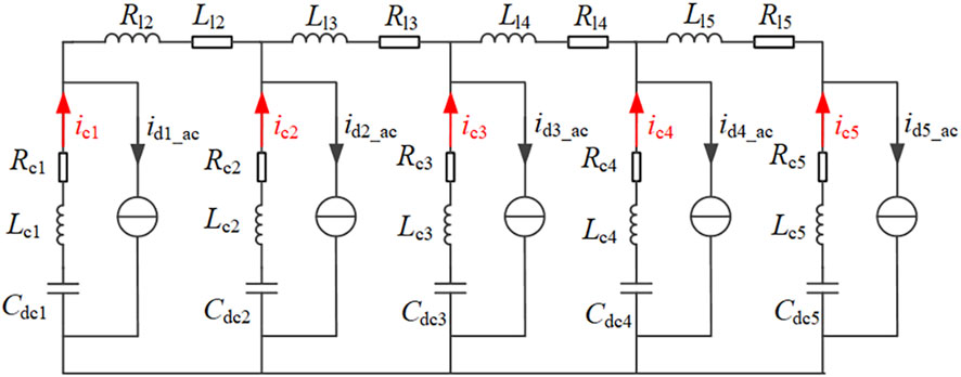
FIGURE 13. Equal circuit of common DC bus five-phase H-bridge converter.
When the phase 1 constant current source id1_ac acts alone, for the k-th harmonic id1h(k) in id1_ac, its angular frequency is ω = 2πkf0, where f0 is the fundamental frequency; similar to Eq. 16, when analyzing the resonance characteristics, the current component ici_d1h(k) of the k-th harmonic id1h(k) on the phase i DC-link capacitors can be found according to the series–parallel relationship of the circuit. Solving the current response of each phase DC-link capacitors under the action of each harmonic in id1_ac and linearly superimposing it, we can obtain the analytical formula of each phase DC-link capacitor current harmonic when the phase 1 constant current source acts alone as follows:
where
The harmonic resolution of each DC-link capacitor current when the five constant current sources act individually is solved separately, and the results of each constant current source are linearly superimposed to obtain the harmonic resolution of each phase DC-link capacitor current when the system works normally, where the phase i DC-link capacitor current is
where
According to Parseval’s theorem, the effective value of the current ripple of each phase DC-link capacitor can be calculated by Eq. 55:
where
A five-phase 4L-NNPC topology H-bridge simulation circuit with multiple DC-link capacitor distributed arrangement structures is built using the MATLAB/Simulink simulation software, and the parameters are shown in Table 1.
TABLE 1. Parameters of the five-phase H-bridge.
The resonance points of the phase 1 DC-link capacitors at this parameter are located near the 54th, 103rd, and 140th harmonic frequencies, which fall near the three carrier side bands of the input current id. The phase 1 DC-link capacitor current ic1 harmonic spectrum is obtained by using the fast Fourier transform of the phase 1 DC-link capacitor current ic1 time domain simulation waveform on a fundamental period. The results are shown in Figure 14A when compared with the theoretical calculation results of Eq. 54. The results of equation calculation and simulation for the remaining four phases of the DC-link capacitor current are shown in Figures 14B–E.
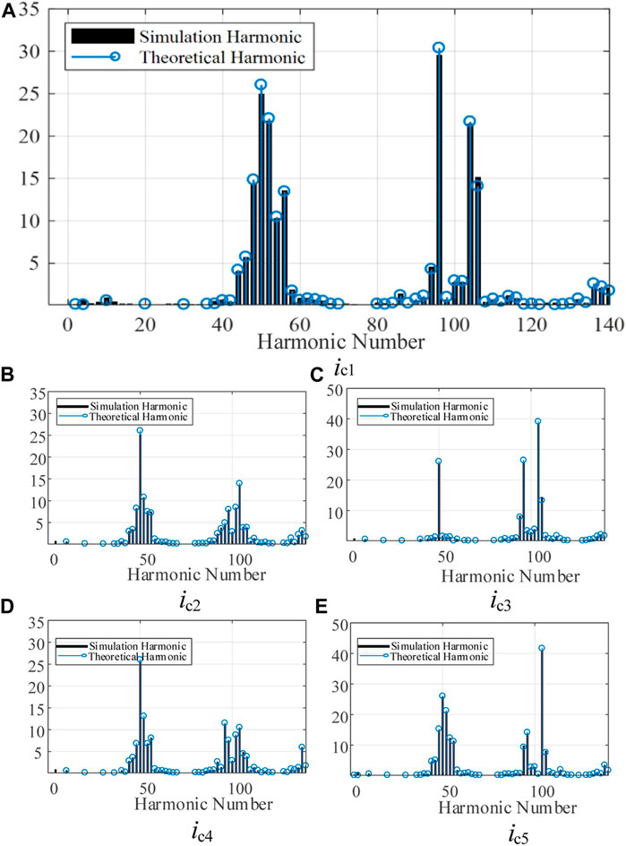
FIGURE 14. Comparison of simulation and theoretical result of harmonic spectra of DC-link capacitor current ic1–ic5. (A) Comparison of harmonic spectra of ic1, (B) Comparison of harmonic spectra of ic2, (C) Comparison of harmonic spectra of ic3, (D) Comparison of harmonic spectra of ic4, (E) Comparison of harmonic spectra of ic5.
The simulation results of the RMS value of the DC-link capacitor current for each phase are compared with the theoretical results calculated according to Eq. 55 as shown in Table 2.
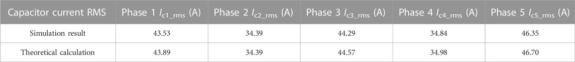
TABLE 2. Comparison of the simulation and theoretical results of the RMS value of the DC-link capacitor current.
It can be seen that the difference between the formula calculation and simulation results of the DC-link capacitor current spectrum is very small, which verifies the correctness of the equivalent circuit of multiple constant-current sources with the distributed arrangement of DC-link capacitors and the analytical formula of the DC-link capacitor current spectrum derived in the previous section.
The distributed arrangement of DC-link capacitors in common DC bus brings the problem of circulating current and resonance. The DC-link capacitors and DC bus parameters determine the resonance characteristics, such as the inherent frequency of the system, resulting in the DC-link capacitor current being directly influenced by several parameters, such as capacitor capacitance size and bus inductance resistance.
Here, we take the first phase DC-link capacitor current RMS value Ic1_rms as an example. According to Eq. 55, when the series equivalent resistance of the DC-link capacitors is 1.4 mΩ and line resistance on the DC bus is 4 mΩ, the surface of the first-phase DC-link capacitor current RMS at different support capacitance C and line inductance on the DC bus Ll is shown in Figure 15. As can be seen from the figure, there are several resonant peak points of the capacitor current RMS, and these resonant peak points should be avoided as much as possible to prevent the DC-link capacitor current from increasing when designing the actual multiphase inverter system.
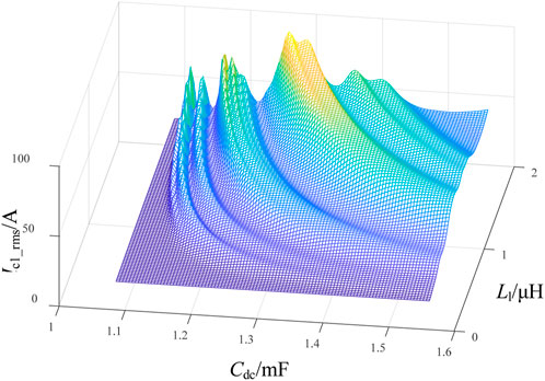
FIGURE 15. RMS value of first phase DC-link capacitor current with different capacitance C and DC bus inductance Ll (Rc = 1.4 mΩ and Rl = 4 mΩ).
This multi-constant current source equivalent circuit method can accurately calculate the resonance points of a multi-phase system, obtain the harmonic analytic formula of the DC-link capacitor current considering the effects of resonance and circulating current, and quantitatively solve the magnitude of the DC-link capacitor current of each phase at resonance. According to this method, the main resonance points of the system can be avoided and the resonance of the DC-link capacitors and busbar inductor can be attenuated during the design, which can effectively guide the selection design of the DC-link capacitors and busbar parameters of the converter with the distributed arrangement of the DC-link capacitors.
5 Conclusion and outlook
According to the principle of DC-link capacitor current analysis methods in converter systems, this work divides the DC-link capacitor current analysis methods into three categories, namely, simulation method, RMS analysis method, and spectral analysis method. The research status, advantages, and disadvantages of the latter two analytical calculation methods are reviewed and summarized one by one, and their detailed calculation process is introduced with the example of a three-phase two-level converter. Then, the general solution of the input current spectrum of the multi-level converter and the characteristics of the multi-phase converter DC-link capacitor current are introduced. To address the problem of resonance with the DC bus when the converter has a distributed arrangement of multiple DC-link capacitors, this work investigates the effect of resonance on the DC-link capacitor current, equates each phase converter unit as a “constant current source” of the input current ripple, and establishes a resonant equivalent circuit of the common DC bus with multiple constant current sources. The resonant characteristics of the system are investigated, and the harmonic analytic formula of the DC-link capacitor current of each phase under resonance is derived, which can be used to guide the selection and design of the DC-link capacitors of converters of related structures. Details of the advantages and disadvantages of the aforementioned strategies and the applicable working conditions are shown in Table 3.
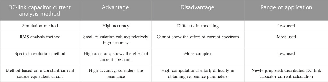
TABLE 3. Comparison of DC-link capacitance current analysis methods.
In the calculation of the DC-link capacitor current, the new energy field has complex working conditions. In photovoltaic power generation and wind power generation, the constant changes in sunlight and wind speed have a great impact on the current ripple stress of the DC-side DC-link capacitors, which must be considered in the actual calculation. Second, distributed multiple DC-link capacitor common DC bus structure converter devices are widely used, so the analysis and calculation of their capacitive resonance problems require the accurate acquisition of DC bus inductance. However, there is no good estimation method for measurement. In addition, the degradation of DC, DC-link capacitors, and other components (such as switching devices) in the converter system will in turn affect the DC-link capacitor current.
With the continuous development of power electronics technology, the selection and design of DC-link capacitors will face the following challenges in the future: 1) fierce competition in the global market. DC-link capacitors have to reduce the redundancy design to compress the cost under the premise of ensuring the system reliability. 2) The power density of converter devices is increasing, and the design of DC-link capacitors is subject to more and more severe volume and heat dissipation constraints. 3) With the wide application of new energy fields and the development of advanced propulsion fields, the future working environment of DC-link capacitors may involve high temperature, sunlight (photovoltaic power generation), high salt and high humidity (vessel propulsion), and other harsh conditions, which puts forward further requirements on its reliability design.
Future research work can be targeted to explore these issues to achieve a more accurate analysis and calculation of the DC-link capacitor current and better guide its selection and design.
Author contributions
CG and BL were responsible for the main writing of the manuscript, while ZX was responsible for the revision of the manuscript. LH provided the ideas and revised the manuscript based on his extensive knowledge and experience in power electronics. All authors have contributed to the article and approved the submitted version.
Funding
This work was supported by the National Natural Science Foundation of China (grant no. 51907200) and the National Defense Strengthening Foundation Plan of China (grant no. 2022-JCJQ-JJ-0537).
Acknowledgments
The authors would like to thank Xin and Associate Researcher Hu for their helpful discussions on topics related to this article.
Conflict of interest
The authors declare that the research was conducted in the absence of any commercial or financial relationships that could be construed as a potential conflict of interest.
Publisher’s note
All claims expressed in this article are solely those of the authors and do not necessarily represent those of their affiliated organizations, or those of the publisher, editors, and reviewers. Any product that may be evaluated in this article, or claim that may be made by its manufacturer, is not guaranteed or endorsed by the publisher.
References
Barth, C. B., Assem, P., Foulkes, T., Chung, W. H., Modeer, T., Lei, Y., et al. (2019). Design and control of a GaN-based, 13-level, flying capacitor multilevel inverter. IEEE J. Emerg. Sel. Top. Power Electron. 8 (3), 2179–2191. doi:10.1109/jestpe.2019.2956166
Basler, B., Greiner, T., and Heidrich, P. “Reduction of DC link capacitor stress for double three-phase drive unit through shifted control and phase displacement,” in Proceedings of the 2015 IEEE 11th International Conference on Power Electronics and Drive Systems, Sydney, NSW, Australia, June 2015, 887–889.
Bierhoff, M. H., and Fuchs, F. W. (2008). DC-link harmonics of three-phase voltage-source converters influenced by the pulsewidth-modulation strategy—an analysis. IEEE Trans. Industrial Electron. 55 (5), 2085–2092. doi:10.1109/tie.2008.921203
Colak, I., Kabalci, E., and Bayindir, R. (2011). Review of multilevel voltage source inverter topologies and control schemes. Energy Convers. Manag. 52 (2), 1114–1128. doi:10.1016/j.enconman.2010.09.006
Cross, A., Evans, P., and Forsyth, A. (1999). DC link current in PWM inverters with unbalanced and non-linear loads. IEE Proceedings-Electric Power Appl. 146 (6), 620–626. doi:10.1049/ip-epa:19990528
Dahono, P. A., Sato, Y., and Kataoka, T. (1996). Analysis and minimization of ripple components of input current and voltage of PWM inverters. IEEE Trans. Industry Appl. 32 (4), 945–950. doi:10.1109/28.511653
Defay, F., Llor, A.-M., and Fadel, M. (2010). Direct control strategy for a four-level three-phase flying-capacitor inverter. IEEE Trans. Industrial Electron. 57 (7), 2240–2248. doi:10.1109/tie.2009.2039457
Delmonte, N., Cabezuelo, D., Kortabarria, I., Santoro, D., Toscani, A., and Cova, P. (2020). A method to extract lumped thermal networks of capacitors for reliability oriented design. Microelectron. Reliab. 114, 113737. doi:10.1016/j.microrel.2020.113737
Diana, M., Guglielmi, P., Piccoli, G., and Rosu, S. G. “Multi-N-phase SMPM drives,” in Proceedings of the 2015 IEEE International Electric Machines & Drives Conference (IEMDC), Coeur d'Alene, ID, USA, May 2015, 1011–1017.
Diana, M., Maqsood, A., Corzine, K., Guglielmi, P., and Parsa, L. (2019). Reducing root-mean-square current stress on the DC link capacitor of a five-phase electric drive through multiple carrier pulse-width modulation technique. IET Electr. Power Appl. 13 (11), 1783–1791. doi:10.1049/iet-epa.2019.0181
Diana, M., Ruffo, R., and Guglielmi, P. (2018). PWM carrier displacement in multi-N-phase drives: An additional degree of freedom to reduce the DC-link stress. Energies 11 (2), 443. doi:10.3390/en11020443
Gasperi, M. L. “Life prediction model for aluminum electrolytic capacitors,” in Proceedings of the IAS'96. Conference Record of the 1996 IEEE Industry Applications Conference Thirty-First IAS Annual Meeting, San Diego, CA, USA, October 1996, 1347–1351.
Gasperi, M. L. (2005). Life prediction modeling of bus capacitors in AC variable-frequency drives. IEEE Trans. Industry Appl. 41 (6), 1430–1435. doi:10.1109/tia.2005.858258
Guo, J., Ye, J., and Emadi, A. (2018). DC-link current and voltage ripple analysis considering antiparallel diode reverse recovery in voltage source inverters. IEEE Trans. Power Electron. 33 (6), 5171–5180. doi:10.1109/tpel.2017.2738327
Hammond, P. W. (1997). A new approach to enhance power quality for medium voltage AC drives. IEEE Trans. industry Appl. 33 (1), 202–208. doi:10.1109/28.567113
Holmes, D. G. “A general analytical method for determining the theoretical harmonic components of carrier based PWM strategies,” in Proceedings of the Conference Record of 1998 IEEE Industry Applications Conference. Thirty-Third IAS Annual Meeting (Cat. No. 98CH36242), St. Louis, MO, USA, October 1998, 1207–1214.
Huiqing, W., Weidong, X., Xuhui, W., and Armstrong, P. (2012). Analysis and evaluation of DC-link capacitors for high-power-density electric vehicle drive systems. IEEE Trans. Veh. Technol. 61 (7), 2950–2964. doi:10.1109/tvt.2012.2206082
Jayakumar, V., Chokkalingam, B., and Munda, J. L. (2021). A comprehensive review on space vector modulation techniques for neutral point clamped multi-level inverters. IEEE Access 9, 112104–112144. doi:10.1109/access.2021.3100346
Kai, L., Mengshu, L., Zhengfeng, L., Zhenghua, D., and Shaoju, T. (2016). Analytical closed-form expressions of DC current ripple for three-level neutral point clamped inverters with space-vector pulse-width modulation. IET Power Electron. 9 (5), 930–937. doi:10.1049/iet-pel.2015.0492
Kieferndorf, F. D., Forster, M., and Lipo, T. A. (2004). Reduction of DC-bus capacitor ripple current with PAM/PWM converter. IEEE Trans. Industry Appl. 40 (2), 607–614. doi:10.1109/tia.2004.824495
Kim, J. S., and Sul, S. K. “New control scheme for AC-DC-AC converter without DC link electrolytic capacitor,” in Proceedings of the IEEE Power Electronics Specialist Conference-PESC'93, Seattle, WA, USA, June 1993, 300–306.
Ko, Y. j., Jedtberg, H., Buticchi, G., and Liserre, M. (2018). Analysis of DC-link current influence on temperature variation of capacitor in a wind turbine application. IEEE Trans. Power Electron. 33 (4), 3441–3451. doi:10.1109/tpel.2017.2704293
Kolar, J. W., and Round, S. D. (2006). Analytical calculation of the RMS current stress on the DC-link capacitor of voltage-PWM converter systems. IEE Proceedings-Electric Power Appl. 153 (4), 535–543. doi:10.1049/ip-epa:20050458
Kumar, L., and Jain, S. (2014). Electric propulsion system for electric vehicular technology: A review. Renew. Sustain. Energy Rev. 29, 924–940. doi:10.1016/j.rser.2013.09.014
Levi, E., Bojoi, R., Profumo, F., Toliyat, H. A., and Williamson, S. (2007). Multiphase induction motor drives – A technology status review. IET Electr. Power Appl. 1 (4), 489. doi:10.1049/iet-epa:20060342
Levi, E. (2008). Multiphase electric machines for variable-speed applications. IEEE Trans. Industrial Electron. 55 (5), 1893–1909. doi:10.1109/tie.2008.918488
Lezana, P., Rodriguez, J., and Oyarzun, D. A. (2008). Cascaded multilevel inverter with regeneration capability and reduced number of switches. IEEE Trans. Industrial Electron. 55 (3), 1059–1066. doi:10.1109/tie.2008.917095
Li, Q., and Jiang, D. (2018). DC-link current analysis of three-phase 2L-VSI considering AC current ripple. IET Power Electron. 11 (1), 202–211. doi:10.1049/iet-pel.2017.0133
Maheswari, K., Bharanikumar, R., Arjun, V., Amrish, R., and Bhuvanesh, M. (2021). A comprehensive review on cascaded H-bridge multilevel inverter for medium voltage high power applications. Mater. Today Proc. 45, 2666–2670. doi:10.1016/j.matpr.2020.11.519
Mantzanas, P., Kuebrich, D., and Duerbaum, T. “Investigation of the DC-link capacitor current ripple in battery-fed PWM inverter systems,” in Proceedings of the 2019 21st European Conference on Power Electronics and Applications (EPE'19 ECCE Europe), Genova, Italy, September 2019.
McGrath, B. P., and Holmes, D. G. (2009). A general analytical method for calculating inverter DC-link current harmonics. IEEE Trans. Industry Appl. 45 (5), 1851–1859. doi:10.1109/tia.2009.2027556
McGrath, B. P., and Holmes, D. G. (2002). An analytical technique for the determination of spectral components of multilevel carrier-based PWM methods. IEEE Trans. industrial Electron. 49 (4), 847–857. doi:10.1109/tie.2002.801071
Mhiesan, H., Wei, Y., Siwakoti, Y. P., and Mantooth, H. A. (2020). A fault-tolerant hybrid cascaded H-bridge multilevel inverter. IEEE Trans. Power Electron. 35 (12), 12702–12715. doi:10.1109/tpel.2020.2996097
Moynihan, J., Egan, M., and Murphy, J. (1998). Theoretical spectra of space-vector-modulated waveforms. IEE Proceedings-Electric Power Appl. 145 (1), 17–24. doi:10.1049/ip-epa:19981564
Nabae, A., Takahashi, I., and Akagi, H. (1981). A new neutral-point-clamped PWM inverter. IEEE Trans. industry Appl. (5), 518–523. doi:10.1109/tia.1981.4503992
Narimani, M., Wu, B., Cheng, Z., and Zargari, N. R. (2014). A new nested neutral point-clamped (NNPC) converter for medium-voltage (MV) power conversion. IEEE Trans. Power Electron. 29 (12), 6375–6382. doi:10.1109/tpel.2014.2306191
Nie, Z., and Schofield, N. (2019). Multi-phase VSI DC-link capacitor considerations. IET Electr. Power Appl. 13 (11), 1804–1811. doi:10.1049/iet-epa.2019.0062
Orfanoudakis, G. I., Yuratich, M. A., and Sharkh, S. M. (2013). Analysis of d-link capacitor current in three-level neutral point clamped and cascaded H-bridge inverters. IET Power Electron. 6 (7), 1376–1389. doi:10.1049/iet-pel.2012.0422
Parsa, L. “On advantages of multi-phase machines,” in Proceedings of the 31st Annual Conference of IEEE Industrial Electronics Society, 2005. IECON 2005, Raleigh, NC, USA, November 2005, 6.
Pei, X., Zhou, W., and Kang, Y. (2015). Analysis and calculation of DC-link current and voltage ripples for three-phase inverter with unbalanced load. IEEE Trans. Power Electron. 30 (10), 5401–5412. doi:10.1109/tpel.2014.2375353
Renken, F. “The DC-link capacitor current in pulsed single-phase H-bridge inverters,” in Proceedings of the 2005 European Conference on Power Electronics and Applications, Dresden, Germany, September 2005.
Rixin, L., Fei, W., Burgos, R., Yunqing, P., Boroyevich, D., Bingsen, W., et al. (2008). A systematic topology evaluation methodology for high-density three-phase PWM AC-AC converters. IEEE Trans. Power Electron. 23 (6), 2665–2680. doi:10.1109/tpel.2008.2005381
Rouhana, N., Semail, E., and Duguey, J.-F. “Impact of PWM strategies on RMS current of the DC-link Voltage Capacitor of a dual-three phase drive,” in Proceedings of the 2014 IEEE Vehicle Power and Propulsion Conference (VPPC), Coimbra, Portugal, October 2014, 1–7.
Su, G.-J., and Tang, L. “A segmented traction drive system with a small dc bus capacitor,” in Proceedings of the 2012 IEEE Energy Conversion Congress and Exposition (ECCE), Raleigh, NC, USA, September 2012, 2847–2853.
Sun, L., Zhenxing, W., Weiming, M., Xiao, F., Cai, X., and Zhou, L. (2014). Analysis of the DC-link capacitor current of power cells in cascaded H-bridge inverters for high-voltage drives. IEEE Trans. Power Electron. 29 (12), 6281–6292. doi:10.1109/tpel.2014.2302081
Tan, L., Wu, B., Narimani, M., Xu, D., Liu, J., Cheng, Z., et al. (2017). A space virtual-vector modulation with voltage balance control for nested neutral-point clamped converter under low output frequency conditions. IEEE Trans. Power Electron. 32 (5), 3458–3466. doi:10.1109/tpel.2016.2589941
Tian, K., Wu, B., Narimani, M., Xu, D., Cheng, Z., and Reza Zargari, N. (2016). A capacitor voltage-balancing method for nested neutral point clamped (NNPC) inverter. IEEE Trans. Power Electron. 31 (3), 2575–2583. doi:10.1109/tpel.2015.2438779
Torki, J., Joubert, C., and Sari, A. (2023). Electrolytic capacitor: Properties and operation. J. Energy Storage 58, 106330. doi:10.1016/j.est.2022.106330
Umesh, B. S., and Sivakumar, K. (2017). Pole-phase modulated multiphase induction motor drive with reduced torque ripple and improved DC link utilization. IEEE Trans. Power Electron. 32 (10), 7862–7869. doi:10.1109/tpel.2016.2634092
Wang, H., and Blaabjerg, F. (2014). Reliability of capacitors for DC-link applications in power electronic converters—an overview. IEEE Trans. industry Appl. 50 (5), 3569–3578. doi:10.1109/tia.2014.2308357
Wang, H., Davari, P., Wang, H., Kumar, D., Zare, F., and Blaabjerg, F. (2018). Lifetime estimation of DC-link capacitors in adjustable speed drives under grid voltage unbalances. IEEE Trans. Power Electron. 34 (5), 4064–4078. doi:10.1109/tpel.2018.2863701
Wang, H., Liserre, M., and Blaabjerg, F. (2013). Toward reliable power electronics: Challenges, design tools, and opportunities. IEEE Ind. Electron. Mag. 7 (2), 17–26. doi:10.1109/mie.2013.2252958
Watanabe, H., Kusaka, K., Furukawa, K., Orikawa, K., and Itoh, J.-I. “DC to single-phase AC voltage source inverter with power decoupling circuit based on flying capacitor topology for PV system,” in Proceedings of the 2016 IEEE Applied Power Electronics Conference and Exposition (APEC), Long Beach, CA, USA, March 2016, 1336–1343.
Welchko, B. A. “Analytical calculation of the RMS current stress on the DC link capacitor for a VSI employing reduced common mode voltage PWM,” in Proceedings of the 2007 European Conference on Power Electronics and Applications, Aalborg, Denmark, September 2007, 1–8.
Williams, B. W. (1986). Power electronics: Devices, drivers and applications. Berlin, Germany: Springer.
Xin, Z., Xiao, F., Hu, L., Wu, W., Lou, X., and Guo, C. (2022). A novel dead-time elimination method for voltage source multilevel converters. IEEE Trans. Power Electron. 38 (2), 1708–1719. doi:10.1109/tpel.2022.3216051
Yan, H., Buticchi, G., Gerada, C., Marquez, A., Leon, J. I., and Liserre, M. “Current harmonic reduction of DC-link capacitor in dual motor drive system,” in Proceedings of the IECON 2019-45th Annual Conference of the IEEE Industrial Electronics Society, Lisbon, Portugal, October 2019, 3148–3153.
Yang, S., Bryant, A., Mawby, P., Xiang, D., Ran, L., and Tavner, P. (2011). An industry-based survey of reliability in power electronic converters. IEEE Trans. Industry Appl. 47 (3), 1441–1451. doi:10.1109/tia.2011.2124436
Yang, S., Lei, Q., Peng, F. Z., and Qian, Z. (2010). A robust control scheme for grid-connected voltage-source inverters. IEEE Trans. Industrial Electron. 58 (1), 202–212. doi:10.1109/tie.2010.2045998
Yang, Y., Wang, H., Sangwongwanich, A., and Blaabjerg, F. (2018). “Design for reliability of power electronic systems,” in Power electronics handbook (Amsterdam, Netherlands: Elsevier), 1423–1440.
Keywords: DC-link capacitors, current calculation, sizing design, resonance, multi-level converter, multi-phase converter
Citation: Guo C, Xin Z, Han J, Hu L and Lu B (2023) Review of the calculation of DC-link capacitor current. Front. Energy Res. 11:1240755. doi: 10.3389/fenrg.2023.1240755
Received: 15 June 2023; Accepted: 24 July 2023;
Published: 08 August 2023.
Edited by:
Farhad Ilahi Bakhsh, National Institute of Technology, Srinagar, IndiaReviewed by:
Andrea Toscani, University of Parma, ItalyQinglei Bu, Xi’an Jiaotong-Liverpool University, China
Copyright © 2023 Guo, Xin, Han, Hu and Lu. This is an open-access article distributed under the terms of the Creative Commons Attribution License (CC BY). The use, distribution or reproduction in other forums is permitted, provided the original author(s) and the copyright owner(s) are credited and that the original publication in this journal is cited, in accordance with accepted academic practice. No use, distribution or reproduction is permitted which does not comply with these terms.
*Correspondence: Jing Han, YW5nZWxoYW5AMTYzLmNvbQ==