 Yue Zhou1
 Yuanzhe Li
- 1Penn Engineering, University of Pennsylvania, Philadelphia, PA, United States
- 2School of Civil and Environmental Engineering, University of Auckland, Auckland, New Zealand
- 3School of Materials Science and Engineering, Nanyang Technological University, Singapore, Singapore
Greenhouse gases (GHGs), particularly fluorinated compounds (FCs), nitrous oxide (N2O), and nitrogen trifluoride (NF3), contribute significantly to climate change, and the semiconductor industry is a notable emitter of these gases. This report introduces an innovative methodology for GHG emission reduction in the semiconductor industry by utilizing advanced abatement systems, referencing Clean Development Mechanism (CDM) published methods AM0078 and AM0111. The proposed methodology shows promising potential, with substantial reductions in FCs, N2O, and NF3 emissions, positioning the semiconductor industry as a key player in climate change mitigation efforts. The main results indicate that by applying the latest abatement systems, a significant reduction in the targeted GHGs can be achieved. The methodology’s verification process confirms the effectiveness of GHG reduction, ensuring that semiconductor manufacturing’s environmental impact is minimized. Our findings suggest that the implementation of this methodology could lead to industry-wide adoption, resulting in a substantial contribution towards stabilizing atmospheric GHG concentrations.
1 Introduction
The 2021 United Nations Climate Change Conference (UNFCCC), also known as COP26, highlighted the urgent need for accelerated action towards the goals of the Paris Agreement and the UN Framework Convention on Climate Change. Climate change is occurring at an unprecedented rate, primarily due to human activities that release greenhouse gases (GHGs) into the atmosphere (Hilaire et al., 2019). In response, countries and parties around the world have launched renewed efforts to combat climate change, with increased carbon reduction targets for 2030 and commitments to achieve net zero emissions by 2050 (Luderer et al., 2018; Rose and Scott, 2020). The semiconductor industry, which plays a significant role in global GHG emissions, has also recognized the need for action (IPCC, 2018). Semiconductor manufacturing, characterized by its energy-intensive processes and use of hazardous gases, contributes to GHG emissions through various stages of production (van Vuuren et al., 2018). As the semiconductor industry continues to grow, its GHG emissions have been on the rise, with major companies emitting millions of tons of carbon annually (Van Vuuren et al., 2013). In response, the industry has sought to develop reduction methods via abatement systems, based on existing UNFCCC Clean Development Mechanism (CDM) methodologies (Van Vuuren et al., 2013; IPCC, 2018; van Vuuren et al., 2018). However, there is a need for further innovation and improvement in reduction methodologies to achieve significant emissions reductions in the semiconductor industry.
In this paper, we propose a new methodology for the significant reduction of fluorinated compounds (FCs) and nitrous oxide (N2O) emissions via an abatement system in the semiconductor industry, building on the Intergovernmental Panel on Climate Change (IPCC) guidelines and existing reduction methods (Van Vuuren et al., 2013). Our methodology focuses on the usage of FCs and selection of abatement systems in the IC manufacturing industry, while recognizing that other aspects of semiconductor production such as materials, photomasks, design, process, packaging, test, and equipment may not be directly applicable (Van Vuuren et al., 2013). Our proposed methodology aims to provide a more effective and efficient approach to reducing GHG emissions in the semiconductor industry, taking into consideration the latest advancements in abatement technologies and best practices for sustainable semiconductor manufacturing.
The implementation of our proposed methodology has significant positive implications for both the environment and the semiconductor industry. By reducing FCs and N2O emissions, which are potent GHGs with long atmospheric lifetimes, our methodology can contribute to mitigating climate change and minimizing “dangerous anthropogenic interference with the climate system,” as stated in the UNFCCC (Smith et al., 2016). Furthermore, our methodology aligns with the increased global efforts to achieve ambitious carbon reduction targets and transition towards a low-carbon economy, as demonstrated by the commitments made by major countries and parties at COP26 (Luderer et al., 2018; Rose and Scott, 2020). Moreover, the semiconductor industry, as a major contributor to global GHG emissions, has a responsibility to adopt sustainable practices and reduce its environmental footprint. Our proposed methodology provides a practical approach for the industry to achieve significant emissions reductions through the adoption of advanced abatement technologies and strategies. Overall, the findings of this paper can contribute to the development of more effective and sustainable GHG reduction methodologies in the semiconductor industry, benefiting both the environment and the industry’s long-term sustainability.
2 Explanation of differences in existing reduction methods
2.1 AM0078: emission reduction via abatement system to reduce SF6 emissions in LCD manufacturing operation
The installation of combustion or thermal abatement equipment to remove SF6 from LCD manufacturing plants is one project activity that can use the emission reduction approach. It aims to reduce SF6 emissions from an LCD etching plant. The reduction project boundary includes SF6 vented into the atmosphere after being used in the LCD etching process, unabated SF6 emission where less than 5% of the SF6 will not be abated via the project, and unabated CO2 emisisons from electricity and fossil fuels used to operate the abatement technology (Czerniak et al., 2007; Van Vuuren et al., 2013). There are a few key requirements that must be met in order for the methodology to be used, such as the absence of any local laws or regulations that require the destruction, recycling, or replacement of SF6 or any component of exhaust gases containing SF6, the destruction of SF6 taking place on the same industrial site where SF6 is used, and the SF6 destroyed not emerging from other facilities (Czerniak et al., 2007).
To ensure accuracy, companies must adhere to quality assurance and quality control (QA/QC) procedures. All monitoring data should be archived electronically and kept for at least 2 years after the last crediting period. Measurements must be conducted with calibrated equipment according to relevant industry standards, and the CDM Project Design Document (CDM-PDD) should include information on the system in place to ensure the quality of the data. This should include actions to be taken to establish and maintain the necessary measurement equipment to meet the requirements for data quality.
2.2 AM0111: emission reduction via abatement system to reduce FCs emissions in preliminary stage semiconductor manufacturing operations
The installation of a fluorinated greenhouse gas (F-GHG) abatement system in an existing semiconductor production plant aims to reduce various greenhouse gases, especially those generated during etching processes within the semiconductor industry. The project’s scope includes F-GHGs, including SF6, emitted from the processes, as well as CO2 emissions from electricity and fossil fuels used to operate the abatement equipment and centralized facilities (Zhu et al., 2023). F-GHGs and SF6 are vented to the atmosphere after being used in the semiconductor etching process. F-GHGs are recovered and destroyed in a catalytic oxidation unit (abatement system) located after the etching unit. There are a few key requirements that must be met before the methodology can be used, such as F-GHGs being vented for at least 3 years prior to the project’s start, no regulations mandating abatement, recycling, or replacement of the project gases, and at least 3 years’ worth of historical data (Hsu et al., 2007).
In order to ensure accuracy, company will have to conform to QA/QC procedures. In the CDM-PDD, project proponents also have to provide information concerning the system in place to ensure the quality of the data. It should include the actions to be undertaken to constitute and to maintain the needed measurement equipment to satisfy the requirements concerning the quality of the data (Tsai et al., 2007). The monitoring methodology will require the project developer to continuously measure all key parameters concerning the operation of the abatement tool and measurement of the baseline and project emissions.
2.3 Summary of old GHG reduction method
Early PFC abatement systems were not effective in destroying CF4, because of its strong C-F molecular bonds. Burn boxes operating at temperatures of 800°C were only up to 27% effective in destroying PFCs. Many times the destruction of CHF3, C2F6, and C3F8 generated CF4 from the decomposition of the original gases (Van Vuuren et al., 2013). The semiconductor manufacturing emission factors include: fluorinated compounds (FCs) that is not destroyed by the emission reduction system; CO2 generated as a by-product of the reduction of F-GHGs; CO2 from the combustion of fossil fuels in the emission reduction system; and CO2 from electricity use during the operation of the emission reduction system. In the monitoring procedure, the gas concentration at the inlet and outlet of the abatement system will be monitored continuously using two FTIR devices and the gas velocity at the inlet and outlet of the abatement system will be monitored continuously as well (Czerniak et al., 2007; Zhu et al., 2023).
The monitoring methodology specifies that the mass of each F-GHG entering and leaving the abatement unit, as well as the inlet and outlet flow rates, should be calculated separately and continuously. The relevant parameters required for the calculation of baseline and project emissions shall be monitored continuously. All measurements shall be carried out using equipment calibrated according to the relevant industry standards. In addition to following the QA/QC and uncertainty assessment procedures for measuring gas concentrations as described in the Baseline section, and the US EPA method for measuring flow rates (Li et al., 2003; IPCC, 2018) In addition to following the QA/QC procedures for measuring gas concentrations as described in the baseline chapter and the QA/QC procedures for measuring flows in the US EPA methodology, the project developer should ensure that maintenance and repair procedures follow, at a minimum, the manufacturer’s recommendations or the requirements specified in this methodology throughout the monitoring period. A record of the maintenance requirements for the monitoring and abatement equipment should be submitted to the verifier.
2.4 Reviews for current methodology & improvement for the raise of semiconductor industry
Table 1 provides information on two different methodologies, AM0078 and AM0111, that are used to reduce greenhouse gas (GHG) emissions in the LCD and semiconductor manufacturing industries. Both methodologies involve the installation of abatement systems in the manufacturing plants, but they target different types of GHG emissions and have different requirements.
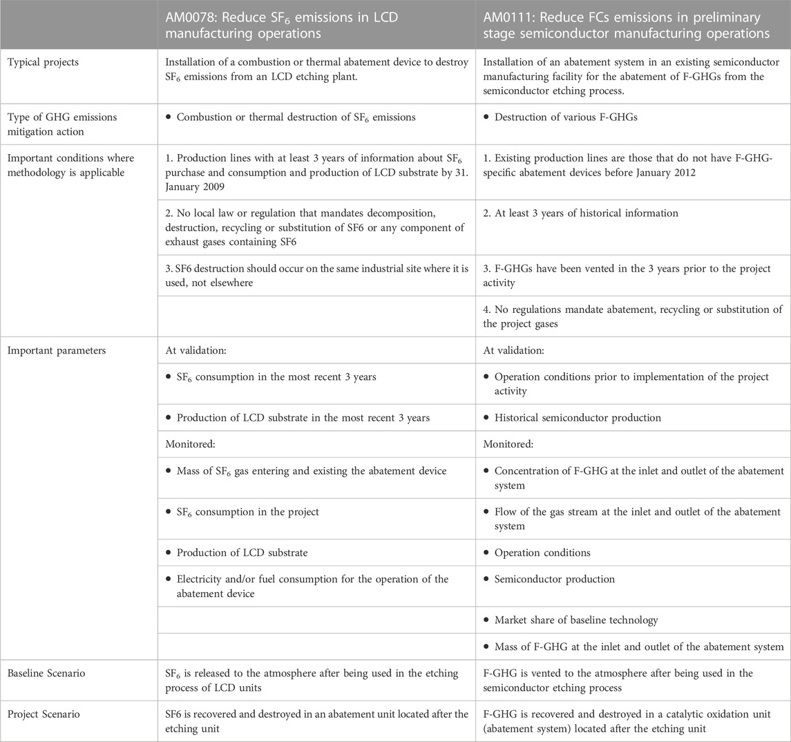
TABLE 1. Important features of the new reduction methods.
AM0078 is designed to reduce sulfur hexafluoride (SF6) emissions in LCD manufacturing operations, and involves the installation of a combustion or thermal abatement device to destroy SF6 emissions from an LCD etching plant. The methodology is applicable to production lines with at least 3 years of information about SF6 purchase and consumption and production of LCD substrate, and there should be no local law or regulation that mandates decomposition, destruction, recycling, or substitution of SF6. The methodology requires the monitoring of SF6 consumption, production of LCD substrate, mass of SF6 gas entering and existing the abatement device, and electricity and/or fuel consumption for the operation of the abatement device.
AM0111, on the other hand, is designed to reduce fluorinated GHG (F-GHG) emissions in preliminary stage semiconductor manufacturing operations, and involves the installation of an abatement system in an existing semiconductor manufacturing facility for the abatement of F-GHGs from the semiconductor etching process. The methodology is applicable to existing production lines that do not have F-GHG-specific abatement devices before January 2012, and there should be at least 3 years of historical information, with F-GHGs vented in the 3 years prior to the project activity, and no regulations mandating abatement, recycling, or substitution of the project gases. The methodology requires the monitoring of concentration and flow of the gas stream at the inlet and outlet of the abatement system, operation conditions, semiconductor production, market share of baseline technology, and mass of F-GHG at the inlet and outlet of the abatement system.
In the baseline scenario, SF6 or F-GHG is released to the atmosphere after being used in the etching process, while in the project scenario, SF6 or F-GHG is recovered and destroyed in an abatement unit or catalytic oxidation unit located after the etching unit (Hsu et al., 2007; Van Vuuren et al., 2013; Zhu et al., 2023). Both methodologies and operational strategies are still relevant for current LCD display manufacturing and low-end wafer or semiconductor manufacturing companies, as supported by references and the fact that F-GHGs are a significant contributor to carbon emissions (Czerniak et al., 2007; Hsu et al., 2007; Tsai et al., 2007; Zhu et al., 2023).
The implementation of the AM0111 and AM0078 methodologies contributes significantly to the reduction of GHG emissions in the semiconductor manufacturing industries. By using abatement systems to destroy F-GHGs and SF6 emissions, these methodologies help to mitigate the impact of greenhouse gases on the environment. The monitoring and reporting of key parameters, such as gas consumption, production, and electricity/fuel consumption, ensure the accuracy and quality of data in the reduction projects. Moreover, the AM0111 and AM0078 methodologies provide a framework for companies to comply with environmental regulations and demonstrate their commitment to sustainable development. As the demand for electronic devices continues to grow, the implementation of these methodologies can help to mitigate the impact of the semiconductor manufacturing industries on the environment and contribute to the global effort to combat climate change (Tsai et al., 2007).
3 New methodology for significant reduction of GHG emissions
3.1 Important features of the new reduction methods
This methodology is specifically applicable to the integrated circuit (IC) manufacturing industry, including processes such as Etching, ThinFilm (chemical/physical vapor deposition), and Diffusion. Other targets such as semiconductor materials (including chemicals), photomasks, design (including Computer Aided Design (CAD) software), manufacturing processes, packaging, testing, and equipment may not fall under the scope of this methodology. The effectiveness of the installed abatement system (Table 2), typically a local scrubber connected to the manufacturing modules, in removing the emissions must be considered, and reference should be made to the guidelines provided by IPCC and US EPA Mandatory Reporting Rule. The destruction removal efficiency (DRE) of the treatment equipment must exceed 90% for combustion, electric, or plasma type systems. For N2O treatment equipment, the DRE should be higher than 60%. In cases where local scrubbers are purchased from external companies, they must be tested upon installation completion.
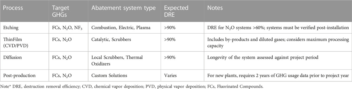
TABLE 2. Overview of new reduction methods for ghg emissions in semiconductor manufacturing.
Furthermore, this methodology is not limited to processes that directly emit fluorinated compounds (FCs), N2O, and NF3 greenhouse gases into the atmosphere, but also encompasses post-production plants with a history of fluorinated and N2O greenhouse gas use and utilization rates for three consecutive years prior to the start of the project year. For post-production new plants, a history of fluorinated and N2O greenhouse gas use and utilization rates for two consecutive years prior to the start of the project year of the installation of proper abatement system is required (Li et al., 2003). The maximum processing capacity of the abatement system must exceed the historical data on the flow of FCs, N2O, and NF3 greenhouse gases into the abatement system, including all other by-products and diluted gases. The reduction project should also assess the lifespan of the abatement system, which must be greater than the project period, and take into account existing equipment that may fail or become obsolete and is no longer applicable for this methodology, or equipment that has been previously used in a reduction project.
The usage rate of fluorinated compounds and N2O greenhouse gases should be calculated based on the amount of gas used (in tons of CO2e) and the wafer production area (in square meters) for the installation of exhaust gas destruction treatment equipment. The wafer size should be defined according to the financial annual report of wafer move, which includes standard sizes such as 5″, 6″, 8″, 12″, and 18″wafers, as well as other applicable sizes. The global warming potential (GWP) gases should follow the guidelines announced by US EPA (Myhre, 2013).
3.2 Installation and technical methodology
The novel methodology integrates a facility-wide SCADA (Supervisory Control and Data Acquisition) system to monitor and manage greenhouse gas (GHG) emissions across the production line. This system is interconnected with an array of pressure transducers strategically installed throughout the production and abatement process. These transducers serve to continuously measure the pressure within the emission stream, ensuring the cleaning of the chemical vapor deposition (CVD) module tool chambers is conducted efficiently. Central to the GHG management are the local scrubbers which treat and significantly reduce emissions before they are released into the atmosphere. These scrubbers operate on advanced combustion, electric, or plasma technologies, ensuring high destruction removal efficiency (DRE) of hazardous gases. The implementation of this system is visually detailed in Figure 1, which illustrates the emission stream flow through the various stages of treatment.
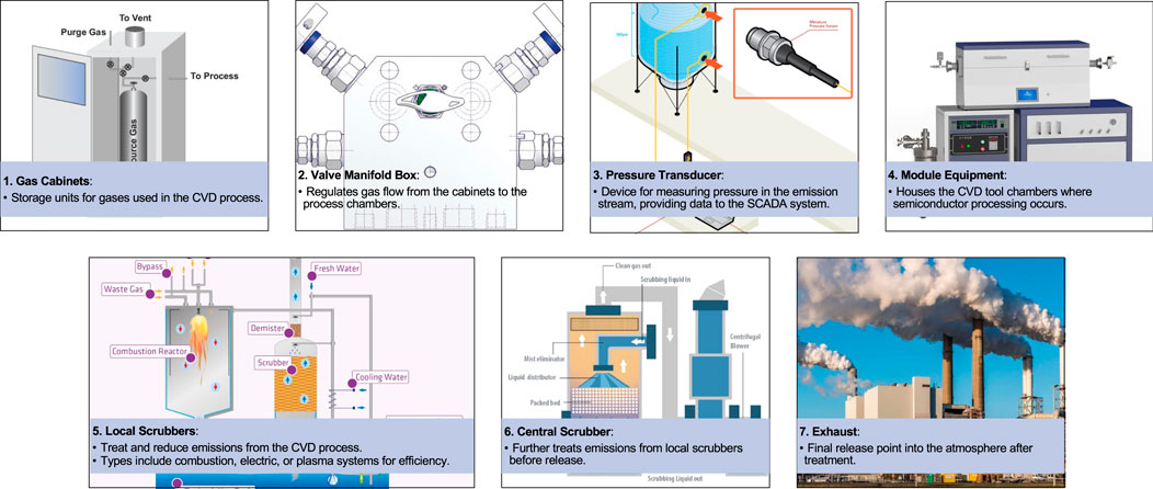
FIGURE 1. Emission stream diagram for cleaning chemical vapor deposition module tool chambers with pressure transducer.
Each emission stream is individually routed to a dedicated local scrubber, facilitating not only a more effective treatment but also allowing for precise emission quantification. This bespoke setup, as shown in Figure 2A, enables one-to-one matching between production systems and abatement mechanisms, thus optimizing the overall efficacy of the GHG reduction. Figure 2B provides an overarching view of the GHG flow, mapping the journey from initial production through to the final emission stage, depicting the systematic approach adopted within the Integrated Pollution Prevention and Control (IPPC) framework.
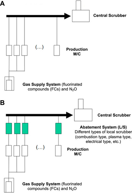
FIGURE 2. Emission stream diagram for cleaning chemical vapor deposition module tool chambers with pressure transducer (A) without local scrubber and (B) with one-to-one connected local scubber (Zhu et al., 2023).
The design of the new methodology methodology is such that each emission stream is connected to one local scrubber so that there will be a more accurate and precise calculation of the emission of FCs. Figure 2 demonstrates the connection method between the production system and abatement system (Zhu et al., 2023). As indicated in Figure 2A, the connection design between production and abatement system (local scrubber) is one to one link up. Whereas, in Figure 2B, the overall mapping for the systematic GHG flow among the IPPU processing is clearly elaborated.
3.3 Calculation approach
The new calculation approach is used to estimate emissions and its by-product by using the “2019 IPCC Guidelines for National Greenhouse Gas Inventories, Volume 3: Industrial Processes and Product Use: Chapter 6 Electronics Industry Emission, Tier 2c” formula. The formula (Eq. 1) for estimation of FC emissions is indicated as below (Myhre, 2013).
Where the Parameter ID and corresponed reporting status has been summarized within the below table (Table 3).
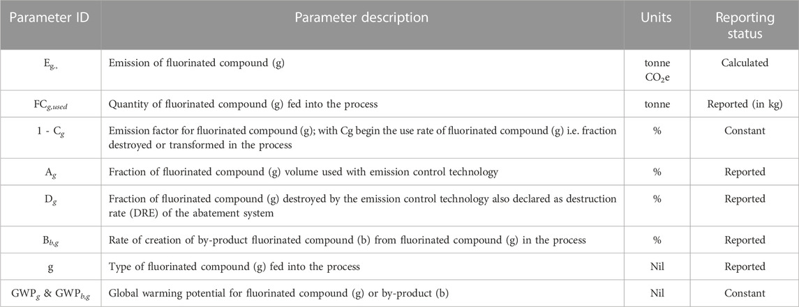
TABLE 3. Parameter ID and corresponed reporting status for Tier 2c formula.
The FCg, used refers to the refers to the quantity of fluorinated compound fed into process; Ag is defined as the fraction of fluorinated compound (g) volume used with emission control technology. It is determined by the design of the abatement system, which takes the considerations of its running mode, maintenance settings, and the connection methodology with the production machine.
The current fraction of fluorinated compound (Dg) destroyed by the emission control technology also declared as destruction rate (DRE) of the abatement system are referred from IPCC 2019 Chapter 6 Table 6.6. Moreover, as more abatement technology is continuously improved and developed, as referred from IPCC 2019, the FTIR testing method with the measurement before and after the local scrubber is acceptable. Semiconductor company may install more abatement system in future and such specifications or testing (i.e., FTIR test) may be obtained from the local scrubber supplier and certified from third party test institution.
4 Basis of preparation and monitoring plan of new reduction method
4.1 Basis of preparation–Activity data
Facility SCADA System - The total amount of each GHG is monitored daily through the SCADA system used in the Facility Department. Data is collected from various sources, such as pressure gauges or weighing scales, and is manually recorded. Records, including tax invoices, delivery orders, technical data sheets, and specifications, are input manually into an Excel file. The file is then checked and verified by a Facility Engineer on a monthly basis. The gas cabinet in the facility is designed with two gas cylinders labeled as “Primary” and “Secondary” supply, which are constantly monitored via the SCADA system. In case of a low detection reading, the system switches to the “Secondary” supply to allow for a cylinder change in the “Primary” supply, ensuring continuous gas supply to the manufacturing process. In the event of instrument failure, the “Secondary” supply is activated and the faulty instrument is replaced. The downtime of the faulty instrument is closely monitored as the gas supply is crucial to the manufacturing process. Spare parts are available for all crucial equipment (Myhre, 2013).
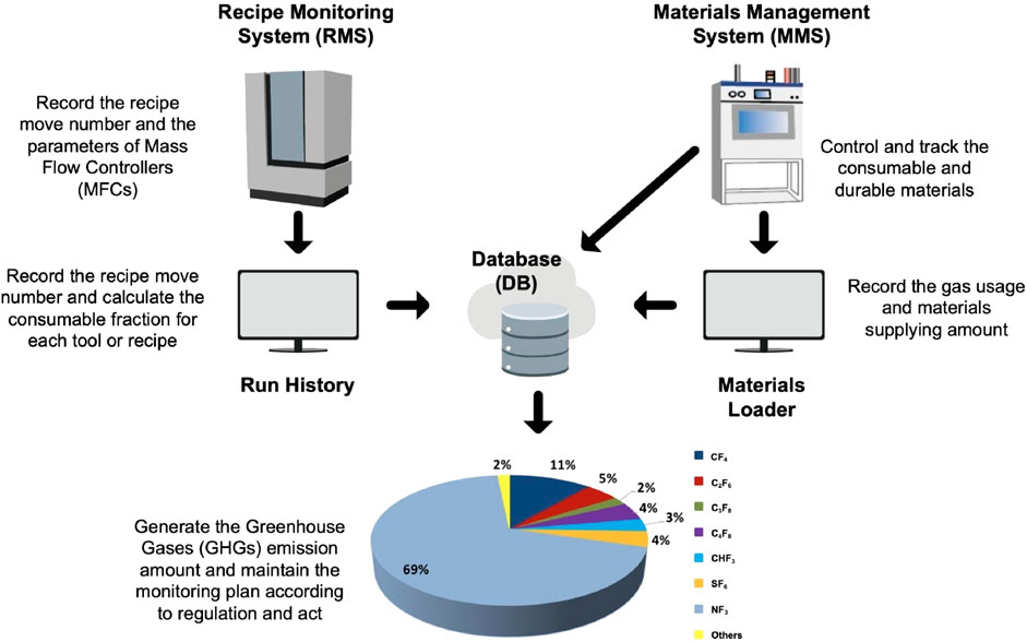
Modules CIM System - For the perfluorocarbons (PFCs), fluor hydrocarbons (HFCs), N2O, SF6 and NF3 used in the process, Etching process, ThinFilm process, include chemical/physical vapor deposition, and Diffusion processes are to provide the settings of flow rate, supply duration, supply frequency, and practical processed wafers for the calculation of the volume usage and the distributed fraction of the HFCs, PFCs and any other GHGs for the previous year before the end of February next year. All relative raw data is able to be retrieved from the Computer Integrated Manufacturing (CIM) System which can provide the relevant usage data on the company’s process GHGs to the departments. Then departments will aggregate the fraction usage of PFCs and HFCs of each machine. Moreover, both departments also need to provide technical information of the exhaust abatement systems together with the gas usage of during the process. Management Department then to calculate the GHG usage of each process. All above mentioned data and calculation will compile and verify the information on a yearly basis. In the future, the CIM system is going to integrate more activity data into the database. All the run history, gas flow and time, gas usage under production as well as maintenance data will be recorded and counted for the GHG consumption as indicated in Figure 3.
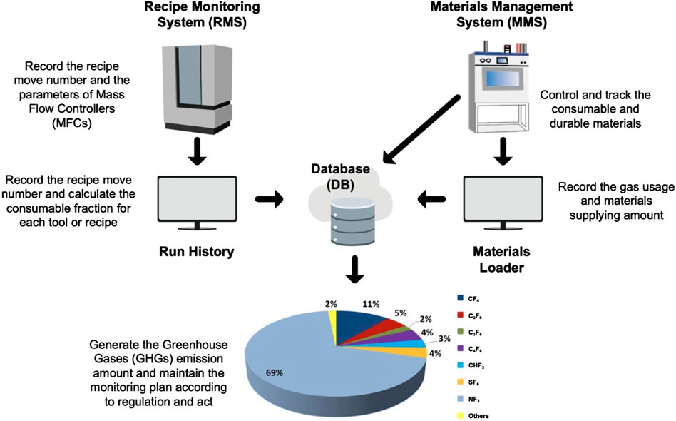
FIGURE 3. The design concept for the Computer Integrated Manufacturing (CIM) system and its implementation.
As illustrated in Table 4, the SCADA system captures comprehensive gas consumption metrics, providing an aggregate measurement of greenhouse gases (GHGs) utilized in the manufacturing process over an annual cycle. It takes into account the total pressure exerted by the gases within the storage containers, which correlates to the mass of GHG consumed. This data, expressed in megapascals (MPa), is essential for calculating the total mass of GHGs emitted, providing a macro-level view of emissions. Conversely, the Computer Integrated Manufacturing (CIM) system offers a granular analysis, detailing the fraction of GHG used by each piece of equipment. This is calculated using parameters such as gas flow rate, supply duration, and wafer throughput, presenting a nuanced understanding of GHG distribution across the production line (Li et al., 2003).
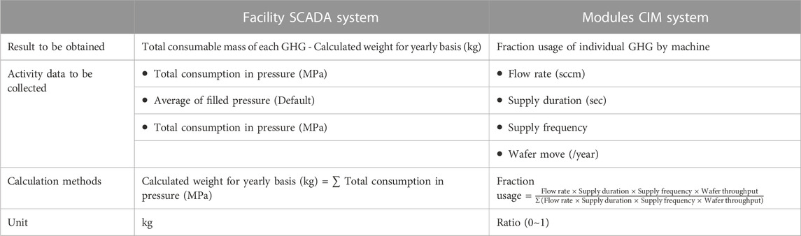
TABLE 4. Activity data, calculation method, and results obtained from SCADA and CIM systems.
Such detailed tracking is crucial in identifying the specific contribution of each module to the facility’s overall GHG footprint, thus enabling targeted emission reduction strategies. The calculation of GHG usage fraction per machine is critical for deploying precise abatement systems, ensuring that the GHG mass flowing into each abatement unit is accurately quantified (Tsai et al., 2007). The combination of SCADA and CIM systems allows for a dual-layered approach to GHG monitoring, encompassing both holistic and detailed perspectives. This dual approach facilitates the application of the Tier 2 method for calculating carbon dioxide equivalent (CO2e) emissions, aligning with international standards for environmental reporting and compliance.
This data acquisition framework is applied within semiconductor manufacturing facilities employing diverse abatement systems to address specific GHGs. Variations in GHG volumes across different production systems necessitate this two-pronged monitoring approach. By capturing both total consumption and individual equipment usage, the framework ensures comprehensive coverage of emission metrics, leading to more informed and effective GHG management strategies (Myhre, 2013; Van Vuuren et al., 2013).
4.2 Monitoring plans
A comprehensive Monitoring Plan (MP) is an integral component mandated for corporations operating facilities with greenhouse gas (GHG) emissions exceeding predefined thresholds. The MP is a strategic document that delineates the GHG emission sources, the associated streams, and the methodologies deployed for emission quantification. This encompasses alternative assessment methods, rigorous quality management protocols, and a detailed analysis of measurement uncertainties, as outlined in Table 5.
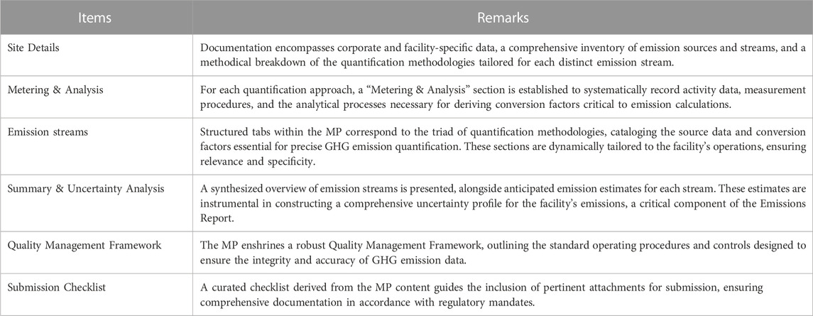
TABLE 5. Key elements to document in the Monitoring Plan (MP).
The enactment of the MP is pivotal for compliance with Monitoring & Reporting (M&R) stipulations and GHG M&R Regulations, facilitating the compilation of the facility’s Annual Emissions Report. The MP, alongside its auxiliary documents encapsulated within the Monitoring Plan Template (‘MP Template’), undergoes a meticulous validation process to ensure the accuracy, reliability, and completeness of the data it presents, aligning with the stringent requirements set forth by environmental regulatory bodies.
4.3 Other consideration factors for the implementation of new reduction methods
In anticipation of installing effective GHG abatement systems, it is imperative for post-production facilities to document a historical record of fluorinated compounds and N2O usage, including utilization rates for at least 2 years prior to project commencement. The abatement system’s processing capacity must surpass historical data trends for the flow of GHGs, accounting for by-products and diluted gases. Moreover, the longevity of the abatement system must be evaluated in the context of the project’s lifespan, taking into consideration the operational viability of existing equipment, and the need for replacement if said equipment has been part of previous GHG reduction initiatives (Myhre, 2013; US EPA, 2023).
5 Future trends and development of semiconductor industry
The semiconductor industry is poised for significant expansion, fueled by a burgeoning demand for consumer electronics and the integration of avant-garde technologies such as artificial intelligence (AI), machine learning (ML), and the Internet of Things (IoT). Projections indicate a surge in market value to USD 820.1 billion by 2028, escalating at a compound annual growth rate (CAGR) of 5.3% from 2021s valuation of USD 550.2 billion. This trajectory is bolstered by macroeconomic factors like increased household income levels, population growth, pervasive digitization, and accelerated urbanization, all converging to escalate the consumption of electronic devices (Oliver et al., 2019).
5.1 Sustainable growth and GHG emissions challenge
Despite this positive outlook, the industry faces the imperative challenge of scaling production sustainably, particularly in light of environmental constraints and the imperative reduction of greenhouse gas (GHG) emissions. The Paris Agreement’s 1.5°C threshold necessitates a global shift towards net-zero emissions by the mid-21st century, implying a balance between emissions produced and those mitigated or offset. Achieving this balance is critical to curtail the progression of climate change and mitigate global warming, which has already resulted in an average temperature rise of approximately 1.1°C since the late 19th century.
5.2 Advanced GHG management in semiconductor fabrication
In semiconductor fabrication facilities or fabs, the use of compressed/clean dry air (CDA) is essential for driving pneumatic systems, managing control valves, and maintaining equipment cleanliness. Efficient monitoring of CDA systems is indispensable for ensuring operational continuity and minimizing downtime. Moreover, adherence to the Intergovernmental Panel on Climate Change (IPCC) guidelines, specifically Chapter 6 addressing Electronics Industry Emissions, is paramount (Wei et al., 2010; Kim et al., 2020). The IPCC provides a systematic framework for accurate GHG emission assessments, offering a variety of methodologies tailored to the unique demands of different segments within the electronics sector (Fthenakis and Kim, 2009). A decision tree assists entities in selecting the most appropriate emission estimation method, taking into account factors such as substrate size in semiconductor manufacturing, thereby enhancing the precision of GHG accounting and enabling informed decision-making for emission reduction strategies (Rogelj et al., 2016).
5.3 Transitioning towards net zero emissions
The semiconductor industry stands at a critical juncture, where it must align its growth trajectory with the global imperative of achieving net zero emissions (Schäfer and Jacobson, 2005). This commitment to carbon neutrality necessitates a paradigm shift in the industry’s operational ethos, extending beyond the implementation of cleaner production technologies. The roadmap to net zero encompasses:
• Strategic Decarbonization: Prioritizing the decarbonization of the energy matrix within semiconductor manufacturing by transitioning to renewable energy sources, such as solar, wind, and geothermal, and investing in carbon capture and storage technologies (Azevedo et al., 2009).
• Supply Chain Optimization: Streamlining supply chains for efficiency and sustainability, reducing emissions from logistics, and incorporating sustainability criteria into vendor selection and management.
• Material Innovation: Embracing material innovations that reduce reliance on high-carbon footprint inputs and exploring the use of sustainable alternatives that offer the same functionality with a lower environmental impact (Li et al., 2023a).
• Energy Management: Implementing comprehensive energy management systems that leverage advanced analytics to optimize energy use and reduce waste in manufacturing processes (Li et al., 2023b).
• Circular Economy Integration: Adopting circular economy principles, such as resource recycling, extending product lifecycles, and designing products for end-of-life recyclability, thereby minimizing waste and the carbon footprint of products.
• Regulatory Compliance and Beyond: Ensuring compliance with evolving environmental regulations, industry standards, and voluntary commitments that aim to reduce GHG emissions across the value chain.
• Stakeholder Engagement and Collaboration: Engaging with government bodies, non-governmental organizations, and industry alliances to collectively develop and adhere to frameworks that facilitate the transition to net zero.
• Investment in Innovation: Continual investment in R&D to develop new technologies and processes that are inherently low-carbon, driving innovation that can deliver emissions reductions at scale.
In pursuit of net zero, the semiconductor industry must also consider the lifecycle emissions of its products, from raw material extraction through to end-user delivery and eventual disposal or recycling (Li et al., 2023b). This holistic view will be instrumental in developing a sustainable pathway that not only aligns with the Paris Agreement but also fosters a resilient and environmentally responsible industry.
6 Conclusion
As the global demand for consumer electronics and cutting-edge technologies continues to grow, the semiconductor industry is projected to expand significantly in the coming years. The market is being driven by rising household incomes, population growth, digitization, and urbanization, among other factors. However, this rapid growth also brings concerns over the sustainability of semiconductor manufacturing and its impact on the environment. While the new reduction method that has been introduced allows for a significant reduction in GHG emissions from semiconductor manufacturing, there is still a long way to go to meet the target of net zero emissions by 2050. Semiconductor manufacturing companies must look into greener alternatives and use more renewable energy sources to achieve sustainable and environmentally responsible growth. By doing so, they can contribute to the global effort to tackle climate change and ensure a sustainable future for generations to come.
Data availability statement
The raw data supporting the conclusions of this article will be made available by the authors, without undue reservation.
Author contributions
YL and YZ make substantial contributions to the conception and design of the work and the acquisition; EO greatly contributes to the analysis and interpretation of the data; YL and YZ draft the work; EO and YL revise it critically for important intellectual content; YL and EO make the final approval of the completed version; YL takes the accountability for all aspects of the work in ensuring that questions related to the accuracy or integrity of any part of the work are appropriately investigated and resolved. All authors contributed to the article and approved the submitted version.
Funding
This research was funded by Enerstay Sustainabiliy Pte Ltd. (Singapore) Grant Call (Call 1/2022) _GHG (Project ID BS-001), Singapore.
Conflict of interest
The authors declare that the research was conducted in the absence of any commercial or financial relationships that could be construed as a potential conflict of interest.
Publisher’s note
All claims expressed in this article are solely those of the authors and do not necessarily represent those of their affiliated organizations, or those of the publisher, the editors and the reviewers. Any product that may be evaluated in this article, or claim that may be made by its manufacturer, is not guaranteed or endorsed by the publisher.
References
Azevedo, I. M. L., Morgan, M. G., and Morgan, K. (2009). The transition to solid-state lighting. Proc. IEEE 97 (3), 481–510. doi:10.1109/jproc.2009.2013058
Czerniak, M. R., Tang, K., and Li, S.-N. (2007). Has the challenge of fluorinated greenhouse gases really been solved? Semiconductor international.
Fthenakis, V., and Kim, H. C. (2009). Land use and electricity generation: a life-cycle analysis. Renew. Sustain. Energy Rev. 13 (6-7), 1465–1474. doi:10.1016/j.rser.2008.09.017
Hilaire, J., Minx, J. C., Callaghan, M. W., Edmonds, J., Luderer, G., Nemet, G. F., et al. (2019). Negative emissions and international climate goals—learning from and about mitigation scenarios. Clim. Change 157 (1-2), 189–219. doi:10.1007/s10584-019-02516-4
Hsu, J.-N., Tsai, C.-J., Chiang, C., and Li, S.-N. (2007). Silane removal at ambient temperature by using alumina-supported metal oxide adsorbents. J. Air & Waste Manag. Assoc. 57 (2), 204–210. doi:10.1080/10473289.2007.10465309
IPCC (2018). Special report on global warming of 1.5 °C. Intergovernmental Panel on climate change. Available at: https://www.ipcc.ch/sr15/.
Kim, S., Hwang, T., Lee, K., and Perrella, R. (2020). Greenhouse gas emissions reduction in different economic sectors: mitigation measures, health co-benefits, and economic impacts. Int. J. Environ. Res. Public Health 17 (4), 1371. doi:10.3390/ijerph17041371
Li, S.-N., Chen, Y.-Y., Shih, H.-Y., Hong, J. L., and Chen, Y. Y. (2003). Using an extractive fourier transform infrared spectrometer for improving cleanroom air quality in a semiconductor manufacturing plant. AIHA J. (Fairfax, Va) 64, 408–414. doi:10.1080/15428110308984835
Li, Y., Qu, Y., Yang, H., Zhou, X., Xiao, P., and Shao, T. (2023a). Combatting biofilms in potable water systems: a comprehensive overview to ensuring industrial water safety. Environ. Microbiol. Rep. 15, 445–454. doi:10.1111/1758-2229.13207
Li, Y., Wang, Y., Chong, D., Xu, Z., Li, L., and Hu, Y. (2023b). Carbon taxation in Singapore’s semiconductor sector: a mini-review on GHG emission metrics and reporting. Carbon Res. 2023, 82. doi:10.1007/s44246-023-00082-0
Luderer, G., Vrontisi, Z., Bertram, C., Edelenbosch, O. Y., Pietzcker, R. C., Rogelj, J., et al. (2018). Residual fossil CO2 emissions in 1.5–2 °C pathways. Nat. Clim. Change 8 (7), 626–633. doi:10.1038/s41558-018-0198-6
Myhre, G. (2013). “Anthropogenic and natural radiative forcing,” in Climate change 2013: the physical science basis. Contribution of working group I to the fifth assessment report of the intergovernmental Panel on climate change (Cambridge: Cambridge University Press). https://www.ipcc.ch/report/ar5/wg1/.
Oliver, G. J., Jubb, A. M., Luhar, A. K., and Mallory, M. L. (2019). The environmental impact of semiconductor manufacturing: technology scaling and its implications for power, water, and chemicals use. Sci. Total Environ. 693, 133569. doi:10.1016/j.scitotenv.2019.07.375
Rogelj, J., Schaeffer, M., Friedlingstein, P., Gillett, N. P., van Vuuren, D. P., Riahi, K., et al. (2016). Differences between carbon budget estimates unravelled. Nat. Clim. Change 6 (3), 245–252. doi:10.1038/nclimate2868
Rose, S., and Scott, M. (2020). Review of 1.5°C and other newer global emissions scenarios: insights for company and financial climate low-carbon transition risk assessment and greenhouse gas goal setting. EPRI. Available at: https://www.epri.com/.
Schäfer, A. I., and Jacobson, M. Z. (2005). Valuation of wind energy on a time-varying basis in California. Renew. Energy 30 (7), 1035–1051. doi:10.1016/j.renene.2004.09.009
Smith, P., Davis, S. J., Creutzig, F., Fuss, S., Minx, J., Gabrielle, B., et al. (2016). Biophysical and economic limits to negative CO2 emissions. Nat. Clim. Change 6 (1), 42–50. doi:10.1038/nclimate2870
Tsai, C.-J., Lin, C.-H., Wang, Y.-M., Hunag, C.-H., Li, S.-N., Wu, Z.-X., et al. (2007). An efficient venturi scrubber system to remove submicron particles in exhaust gas. Air & Waste Manag. Assoc. 55 (3), 319–325. doi:10.1080/10473289.2005.10464622
US EPA (2023). Greenhouse gas mandatory reporting Rule, subpart I, electronic code of federal regulations, table I-16 to subpart I of Part 98—default emission destruction or removal efficiency (DRE) factors for electronics manufacturing. Available at: https://www.ecfr.gov/current/title-40/chapter-I/subchapter-C/part-98/subpart-I/appendix-Table%20I-16%20to%20Subpart%20I%20of%20Part%2098.
Van Vuuren, D. P., Deetman, S., van Vliet, J., van den Berg, M., van Ruijven, B. J., and Koelbl, B. (2013). The role of negative CO2 emissions for reaching 2 °C— insights from integrated assessment modelling. Clim. Change 118 (1), 15–27. doi:10.1007/s10584-012-0680-5
van Vuuren, D. P., Stehfest, E., Gernaat, D. E. H. J., van den Berg, M., Bijl, D. L., de Boer, H. S., et al. (2018). Alternative pathways to the 1.5 °C target reduce the need for negative emission technologies. Nat. Clim. Change 8 (5), 391–397. doi:10.1038/s41558-018-0119-8
Wei, M., Patadia, S., and Kammen, D. M. (2010). Putting renewables and energy efficiency to work: how many jobs can the clean energy industry generate in the US? Energy Policy 38 (2), 919–931. doi:10.1016/j.enpol.2009.10.044
Keywords: greenhouse gas (GHG), GHG emission reduction, removal methodology, semiconductor industry, gas abatement system
Citation: Zhou Y, Li Y and Ong E (2024) Advancements in greenhouse gas emission reduction methodology for fluorinated compounds and N2O in the semiconductor industry via abatement systems. Front. Energy Res. 11:1234486. doi: 10.3389/fenrg.2023.1234486
Received: 04 June 2023; Accepted: 14 December 2023;
Published: 05 January 2024.
Edited by:
Anna Stoppato, University of Padua, ItalyReviewed by:
Diana D’Agostino, University of Naples Federico II, ItalyCopyright © 2024 Zhou, Li and Ong. This is an open-access article distributed under the terms of the Creative Commons Attribution License (CC BY). The use, distribution or reproduction in other forums is permitted, provided the original author(s) and the copyright owner(s) are credited and that the original publication in this journal is cited, in accordance with accepted academic practice. No use, distribution or reproduction is permitted which does not comply with these terms.
*Correspondence: Yuanzhe Li, eXVhbnpoZTAwMUBlLm50dS5lZHUuc2c=